Efficient and photostable CsPbI2Br solar cells realized by adding PM MA
Yanbo Shang ,Zhimin Fang ,Wanpei HuChuantian ZuoBairu LiXingcheng LiMingtai Wang,Liming Ding ,and Shangfeng Yang
1Hefei National Laboratory for Physical Sciences at Microscale,Key Laboratory of Materials for Energy Conversion (CAS),Anhui Laboratory of Advanced Photon Science and Technology,Department of Materials Science and Engineering,University of Science and Technology of China,Hefei 230026,China
2Center for Excellence in Nanoscience (CAS),Key Laboratory of Nanosystem and Hierarchical Fabrication (CAS),National Center for Nanoscience and Technology,Beijing 100190,China
3Institute of Solid State Physics,Chinese Academy of Sciences,Hefei 230031,China
Organic–inorganic hybrid perovskite materials demonstrate promising applications in high-efficiency perovskite solar cells (PSCs) with a certified power conversion efficiency(PCE) of 25.5% (https://www.nrel.gov/pv/cell-efficiency.html).However,intrinsically volatile and thermally unstable nature of the organic cations result in poor thermal stability of organic–inorganic hybrid perovskite materials,hampering the commercialization of organic-inorganic hybrid PSCs[1].All-inorganic CsPbI3–xBrx(x=0–3) perovskites have been attracting great attention in recent years because of their higher thermal stability[2].Among the reported CsPbI3–xBrxperovskites,CsPbI2Br bears a reasonable balance between bandgap and phase stability,thus becomes the most extensively studied material[3−15].Though there are many works aiming at achieving high-efficiency CsPbI2Br PSCs,improving the photostability of CsPbI2Br PSCs is another key for commercialization of all-inorganic PSCs.Intriguingly,it has been reported that CsPbI2Br is susceptible to make light-induced phase segregation,i.e.severe segregation of CsPbI2Br to low-bandgap I-rich and wide-bandgap Br-rich domainsviaion diffusion,leading to obvious current–voltage hysteresis and decrease of stabilized power output (SPO)[16−20].Such a light-induced phase segregation can be suppressed by optimizing the interface between perovskite layer and charge-transport layer[18,19].For example,Tianet al.improved the photostability of CsPbI2Br PSCs through modifying SnO2electron-transport layer by PN4N and incorporating dopant-free PDCBT hole-transport layer[18].Xiaoet al.developed a new dopant-free holetransport layer PSQ2 to substitute Spiro-OMeTAD,and found that PSQ2-based devices had less SPO loss[19].Despite of the effectiveness of suppressing light-induced phase segregationviasuch interfacial modification,whether the phase segregation is induced merely by light illumination or already exists in the crystallization of CsPbI2Br remains unclear yet.Another open question is whether the photostability of CsPbI2Br can be improved by eliminating light-induced phase segregation of CsPbI2Br via modulating the crystallization process of CsPbI2Br.
Here,we introduced poly(methyl methacrylate) (PMMA)additive into CsPbI2Br to modulate the crystallization process of perovskite films.We found that phase segregation occurs during crystallization of CsPbI2Br especially under fast crystallization rate and low annealing temperature,and this intrinsic phase segregation exacerbates light-induced phase segregation.With PMMA additive,CsPbI2Br solar cells gave an enhanced PCE of 15.88%,and the photostability was improved.
We added PMMAviaanti-solvent dripping (Fig.S1)[21].The CsPbI2Br film with PMMA exhibited slow color change from transparent to brown-yellow during annealing (Fig.S2),indicating that PMMA incorporation leads to slower crystallization of CsPbI2Br and larger grain with reduced root-meansquare (RMS) roughness.(Fig.1(a),Figs.S3 and S4).The crystallinity and crystalline orientation of CsPbI2Br film were also optimized.XRD shows that CsPbI2Br film with 0.05 mg/mL PMMA has strongest (100) and (200) diffraction peaks(Fig.S5).The GIXRD patterns reveal the improved orientation of CsPbI2Br crystal with (100) and (200) planes parallel to the substrate (Figs.S6 and S7).PMMA incorporation improves the crystalline orientation of CsPbI2Br along plane(100) (Fig.1(b)).
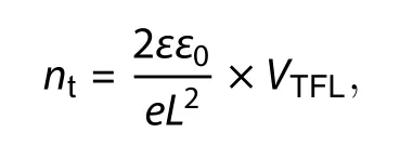
We studied the trap-state density (nt) of CsPbI2Br layer by using space charge limited current (SCLC) method based on an electron-only device with a structure of ITO/SnO2/ZnO/perovskite/PCBM/Ag (Fig.1(c))[22].ntcan be calculated by equation:

whereε0is the vacuum permittivity,εis the relative dielectric constant of CsPbI2Br[13],eis the elementary charge,andLis the thickness of perovskite film.The trap-filled limit voltage(VTFL) is the bias voltage at the kink point.Thentdecreased from 1.09 × 10¹⁶to 8.18 × 1015cm−3after PMMA incorporation.Low trap density favors to reduce charge recombination.The carrier lifetimes (τ) of CsPbI2Br films measured by time-resolved photoluminescence (TRPL) were 6.68 and 10.34 ns for the control film and the film with PMMA,respectively (Fig.S8,Table S1)[23].The prolonged carrier lifetime suggests that PMMA can passivate trap states.The higher intensity of the PL peak for CsPbI2Br film (Fig.S9),smaller ideal factor (ε) obtained fromVocvs light intensity plots (Fig.S10),and decreasedRct(charge transfer resistance) obtained from EIS (Fig.S11 and Table S2) all suggest suppressed non-radiative decay in CsPbI2Br film with PMMA.

Fig.1.(Color online) (a) Cross-section SEM image for CsPbI2Br solar cell.(b) Schematic illustration of perovskite crystal with and without PMMA.(c) Dark current–voltage curves for the electron-only devices with and without PMMA.(d) Stabilized power output (SPO) of CsPbI2Br device with PMMA.(e) Steady-state PL spectra for CsPbI2Br films from different fabrication process (annealed at 100 °C).(f) Steady-state PL spectra for CsPbI2Br films with PMMA before and after illumination.
PSCs with a structure of ITO/SnO2/ZnO/CsPbI2Br/Spiro-OMeTAD/MoO3/Ag were made.The photovoltaic performances for the devices with and without PMMA were compared (Fig.S12,Fig.S13 and Table S3).The PCE increased from 14.42% to 15.88% after adding 0.05 mg/mL PMMA.The negligible change ofJscis verified by external quantum efficiency (EQE) measurements (Fig.S14).The PCE enhancement for the device with PMMA results from the increases ofVoc(1.124 to 1.216 V) and FF (67.77% to 75.28%),which can be attributed to decreased trap states in CsPbI2Br film with PMMA.The devices with PMMA have smaller hysteresis index (Fig.S15 and Table S4) and less degradation of SPO (Fig.1(d) and Fig.S16(a))[18,19].The existence of hysteresis and SPO degradation suggest the occurrence of light-induced phase segregation of CsPbI2Br[19,20].The smaller hysteresis and SPO degradation suggest that PMMA can suppress light-induced phase segregation of CsPbI2Br.

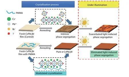
Fig.2.(Color online) The proposed mechanism for the elimination of phase segregation in CsPbI2Br film by PMMA.
Without PMMA,the phase segregation of CsPbI2Br takes place during the formation of CsPbI2Br film,and we call it intrinsic phase segregation.On the one hand,intrinsic phase segregation occurs more easily at low annealing temperature.The best devices we discussed above were all made at 240 °C.However,CsPbI2Br PSCs made under 100 °C exhibit more serious degradation of SPO (Fig.S16(b)) and larger hysteresis index (Table S4),indicating more severe phase segregation.Low annealing temperature does not favor the growth of homogeneous inorganic perovskite films,which are commonly made at high temperature.But,with PMMA incorporation,hysteresis and SPO degradation (Fig.S16(c)) were suppressed effectively even at low temperature.On the other hand,insufficient components diffusion could occur at fast crystallization rate,which results in phase segregation eventually.Usually,perovskite precursors with DMF solvent exhibit fast crystallization rate,while DMSO could slow down the crystallization[24].When using DMF/DMSO mixed solvent,PL peak split indicates that phase segregation becomes less obvious.PMMA retards the crystallization (Fig.S2),leading to single PL peak,suggesting the elimination of intrinsic phase segregation (Fig.1(e)).
Light-induced phase segregation is caused by ion migration,and the smaller Br–ions are easier to migrate than I–.With higher Br content,the phase segregation takes place easily[25].Intrinsic phase segregation generates I-rich phase and Br-rich phase,and this uneven composition will exacerbate phase segregation.According to SEM images (BSE mode)(Fig.S17),more uniform grain color reveals suppressed phase segregation.After 45 min illumination,no PL peak split and GIXRD (200) diffraction peak were observed for CsPbI2Br film with PMMA (Fig.1(f),Fig.S18 and Fig.S19)[9],indicating that light-induced phase segregation was suppressed by PMMA.We further evaluated the photostability of CsPbI2Br devices under continuous illumination (unencapsulated in N2glovebox).A~36% PCE drop was observed for the control device after 400 h operation,while for PMMA-containing device,the PCE droped by~17% (Fig.S20(b)).The improved photostability was due to the elimination of phase segregation.
We propose a mechanism for the elimination of phase segregation in CsPbI2Br film by using PMMA (Fig.2).The coordination interactions between C=O groups in PMMA and Pb2+in CsPbI2Br (Fig.S21 and Fig.S22) lead to lowered crystallization rate,making uniform distribution of I–and Br–anions[21].The intrinsic phase segregation is eliminated at low annealing temperature and this prohibition effect is expected to exist under light illumination as well,resulting in suppressedJ–Vhysteresis and eliminated light-induced phase segregation.
In summary,PMMA was added into CsPbI2Br layer to modulate the crystallization and eliminate the phase segregation.PMMA can also passivate the trap states.The CsPbI2Br solar cells delivered an enhanced PCE of 15.88% and an improved photostability.
Acknowledgements
This work was supported by the National Key Research and Development Program of China (2017YFA0402800),National Natural Science Foundation of China (51925206,U1932214),and Collaborative Innovation Program of Hefei Science Center (2020HSC-CIP004).L.Ding thanks the National Key Research and Development Program of China(2017YFA0206600) and the National Natural Science Foundation of China (51773045,21772030,51922032,21961160720)for financial support.
Appendix A.Supplementary materials
Supplementary materials to this article can be found online at https://doi.org/1674-4926/42/5/050501.
 Journal of Semiconductors2021年5期
- Journal of Semiconductors的其它文章
- Intramolecular spatial charge transfer enhances TADF efficiency
- Fiber-like solar cells
- Over 1 cm2 flexible organic solar cells
- S urface-enhanced Raman spectroscopy chips based on twodimensional materials beyond graphene
- Drop-coating produces efficient CsPbI2Br solar cells
- Recent progress of physical failure analysis of GaN HEMTs
