
Molecular beam epitaxy growth of iodide thin films∗
2021-03-11 08:34:12XinqiangCai蔡新强ZhilinXu徐智临ShuaiHuaJi季帅华NaLi李娜andXiChen陈曦
Chinese Physics B 2021年2期
Xinqiang Cai(蔡新强), Zhilin Xu(徐智临), Shuai-Hua Ji(季帅华), Na Li(李娜), and Xi Chen(陈曦)
1State Key Laboratory of Low Dimensional Quantum Physics,Department of Physics,Tsinghua University,Beijing 100084,China
2Key Laboratory for the Physics and Chemistry of Nanodevices,Department of Electronics,Peking University,Beijing 100871,China
Keywords: two-dimensional magnetism, iodide thin films, molecular beam epitaxy, scanning tunneling microscope
Since the discovery of graphene in 2004, twodimensional(2D)materials have been extensively studied because of their fascinating properties and potential applications in fabricating functional nanomaterials and nanodevices.[1,2]Among the various properties,2D magnetism has drawn great attention recently. The investigation on the long-range magnetic order and other spin-related phenomena at the 2D limits may promote the development of spintronics at the nano-scale.
The 2D magnetism was first clearly confirmed in atomically thin CrI3[3]and Cr2Ge2Te6[4]layers, respectively. The high-quality 2D magnetic crystals are mechanically exfoliated from the layered compounds. However, the size and yield of the flakes from exfoliation potentially limit further applications. Chemical vapor deposition(CVD)is another approach to synthesize the 2D magnetic materials.In addition,it is difficult to avoid the contamination introduced in the process of exfoliation or deposition. Here we consider the molecular beam epitaxy (MBE) growth of iodides with promising long-range magnetic order in 2D limit. MBE growth in ultrahigh vacuum(UHV)can achieve much higher purity under well-controlled conditions.
In the MBE synthesis of iodides,one needs metal and iodine sources with high purity. However,the vapor pressure of elemental iodine I2at room temperature is as high as 0.2 torr,which is not compatible with UHV. A leak valve can be employed to dose such substance with high vapor pressure.[5]Herein we introduce a more convenient and reliable procedure to generate I2molecular beam, in which I2is thermally decomposed from pure iodides,similar to previous attempt to use FeS as sulfur source.[6]By heating selected iodides in Knudsen cell,it is possible to obtain sufficient flux of I2. Compared with the gaseous source,the I2vapor from decomposition can be fine-controlled. Such procedure is universally applicable in MBE growth of iodides and can well protect the vacuum system. To demonstrate the advantage of the compound iodine source, we prepare MnI2, GdI3, and CrI2thin films down to monolayer. Further studies are needed to reveal the magnetic properties of these iodides.
The experiments were conducted on a Unisoku lowtemperature scanning tunneling microscope (STM) equipped with an MBE chamber. After thin film preparation, the samples were directly transferred to STM at 78 K for characterization. The STM topographic imaging at the atomic scale was utilized to identify the crystal structures. The local density of states was measured by the scanning tunneling spectroscopy(STS) to unveil the electronic structure of the samples. Before STM measurement,the Pr–Ir alloy tips were checked and modified on the surface of Ag(111)islands grown on Si(111).The samples can also be transferred to x-ray photoelectron spectroscopy(XPS)to analyze the chemical compositions.
A good candidate for the compound iodine source needs to be stable in air and its decomposition products except I2should have exceedingly low vapor pressure. Furthermore,the decomposition temperature for stably producing adequate amount of I2vapor has to be high enough (usually above 200◦C) in order for the Knudsen cell to work in the temperature range with precise control. Among various iodides,VI3and CrI3[7–10]are found to meet the requirements. After heating,they are decomposed into I2vapor together with solid VI2or CrI2[9,10]following the formula 2MI3(s)⇋2MI2(s)+I2(g),where M represents V or Cr.We choose CrI3powder(Six Carbon Technology) as the I2source in the MBE growth. The Knudsen cell uses Al2O3crucible. According to previous report,[9]the equilibrium pressure of I2vapor in the reaction 2CrI3⇋2CrI2+I2satisfies log[P(torr)]=−8936/T+11.832,when the heating temperature T is between 580 K and 650 K.Extrapolation to the temperature slightly below 580 K sets the upper limit of I2vapor pressure as 10−6torr at 230◦C and 10−5torr at 260◦C.The working temperature of the Knudsen cell in our MBE growth is around this range, where the sensitivity of the vapor pressure to temperature is low enough to ensure a stable I2flux.
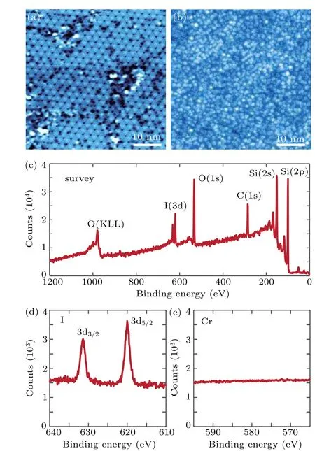
Fig.1. STM topography (50 nm×50 nm, bias: 1.5 V, current: 20 pA) of(a) Si(111) surface with 7×7 reconstruction before deposition. (b) I2 on Si(111) surface after deposition. (c) XPS survey of adsorbates on Si(111)surface. (d)XPS signal of iodine 3d electrons. (e)Absence of XPS signal of chromium 2p electrons.
The I2source was checked by deposition onto clean Si(111)surface with 7×7 reconstruction structure obtained by flashing to 1180◦C for several times. The temperature of the Knudsen cell was kept at 220◦C and the pressure was below 3×10⁻⁹torr during the growth.Figures 1(a)and 1(b)show the STM topographic images of Si(111) before and after deposition, respectively. The adsorbates are clearly revealed. Besides iodine,the adsorbates could be the unwanted Cr,CrI2,or CrI4(similar to VI3, decomposition accompanied by gaseous VI4[9]). The composition of the adsorbates was analyzed by XPS.Figure 1(c)exhibits the XPS spectrum,where peaks corresponding to I,Si,C,and O are clearly identified. The carbon and oxygen come from the air contamination because of the ex-situ XPS measurement. The two peaks in Fig.1(d) at energies of 631.4 eV and 620.0 eV well match the characteristic photoemission spectra of 3d3/2and 3d5/2states for I2.[11]No Cr(2p)characteristic peaks[12]have been detected(Fig.1(e)).Generally,CrI3is an eligible source of iodine in MBE thin film growth.
Three typical iodides MnI2, GdI3, and CrI2with layered Van der Waals structure have been prepared by using the CrI3source. The three compounds are chosen according to their magnetic properties in their bulk form, which are antiferromagnetic below 3.95 K for MnI2,[13,14]possibly antiferromagnetic below 1.5 K for GdI3,[15]and unexplored for CrI2. We mainly like to focus on the antiferromagnetic materials due to recent advent of antiferromagnetic spintronics.[16–18]Devices made of antiferromagnetic materials are stable against external magnetic field and have little influence on the devices nearby.For the purpose of device applications, it is indispensable to prepare antiferromagnetic thin films with high quality.
In the experiments, the Mn, Gd, or Cr metals (Alfa Aesar, purity over 99.9%) were evaporated from Knudsen cells.The co-deposited metal atoms and I2molecules react to form thin films on graphitized 6H-SiC(0001) (n-doped, resistivity~0.1 Ω·cm)substrate kept at elevated temperature. The substrate is terminated with monolayer or bilayer graphene by heating to 1400◦C in advance. During growth, the pressure was below 3×10⁻⁹torr. The nominal flux of iodine is much higher than that of the metal atoms(the ratio is over 10:1)to ensure sufficient reaction on the substrate surface.
Figure 2 shows the growth and characterization of MnI2films down to monolayer. Bulk MnI2is antiferromagnetic and ferroelectric at low temperature, with a polarization direction tunable by magnetic field.[19]Figure 2(a) exhibits the crystal structure of MnI2, which is isostructural to CdI2. The lattice constants are a=b=4.146 ˚A, and c=6.829 ˚A.[13]The MBE growth of MnI2film helps to study the magnetic order and multiferroicity at 2D limit. To achieve high quality MnI2films,the temperatures of Mn and CrI3sources were set at 680◦C and 236◦C, respectively, while the substrate at 210◦C. Figure 2(b) shows the STM topography of a sample after 60 min of deposition. Edge of the monolayer films is highlighted by yellow lines. The triangular lattice is observed in the atomic resolution STM image(Fig.2(c)). The in-plane lattice constants are measured to be a=b=4.14 ˚A.The apparent height of the MnI2monolayer above graphene is 6.8 ˚A(inset of Fig.2(b)). The measured lattice parameters well match those of the bulk material. Further STS measurement(Fig.2(d)) demonstrates that monolayer MnI2is an insulator with a bandgap of about 4.4 eV.
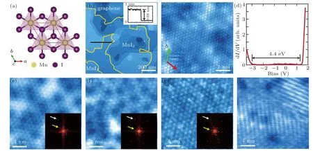
Fig.2. (a) Top view of single layer MnI2. I atoms above and below Mn atomic plane form two triangular lattices. (b) STM topography of MnI2 films(1000 nm×1000 nm;bias:3 V;current:20 pA).Edge of MnI2 film is highlighted by yellow line. Inset shows the height profile along the black line. (c)STM atomic resolution of MnI2 (10 nm×10 nm;bias: 1 V;current: 100 pA).(d)STS of monolayer MnI2 (bias: 1.7 V;current: 100 pA).(e)–(g)STM images(20 nm×20 nm;bias: 1.9 V(e),1.8 V(f),−0.5 V(g);current: 100 pA)of Moir´e patterns on monolayer MnI2 with FFT inset.The periods are 1.19 nm,1.28 nm,and 1.32 nm,respectively. (h)STM image of stripe pattern on monolayer MnI2 (bias: 1.5 V;current: 100 pA).
Monolayer MnI2on bilayer graphene exhibits various Moir´e patterns depending on the twisted angles between MnI2and graphene. Three types of Moir´e patterns are clearly resolved in the STM images (Figs. 2(e)–2(g)). In the corresponding fast Fourier transform(FFT,see the insets),the peaks arising from the triangular lattice and the Moir´e patterns are indicated by white and yellow arrows. The periods and the twisted angles relative to graphene of the three Moir´e patterns are 1.19 nm, 1.28 nm, 1.32 nm and 5.0◦, 2.5◦, 1.0◦, respectively. Occasionally, a twisted angle as large as 30◦is also observed(not shown). Apart from the Moir´e patterns,monolayer MnI2sometime shows a stripe structure(Fig.2(h))with period between 1.12 nm and 1.20 nm. The orientation of the stripes has no obvious relation with the lattice and the edge of the film. The origin of the stripe structure is not understood yet.
Figure 3 shows the growth and characterization of GdI3films down to monolayer. Bulk GdI3is isostructural to BiI3.A unit cell contains three single-layers of GdI3. A single layer of GdI3has one layer of Gd sandwiched between two layers of I atoms as shown in Fig.3(a). The lattice parameters are a=b=7.539 ˚A and c=20.83 ˚A.[20]The GdI3film in Fig.3(b) took 30 min to prepare under the condition of Gd source at 1080◦C,CrI3at 225◦C,and the substrate at 500◦C.The growth window of the substrate temperature is rather large and can be as low as 300◦C.As shown in the atomic resolution STM image in Fig.3(c),the Gd atoms form a honeycomb lattice. The in-plane lattice constant is measured to be 7.54 ˚A and is consistent with that of bulk GdI3.The apparent height of GdI3monolayer above graphene is 6.5 ˚A(inset of Fig.3(b)),which is close to c/3=6.94 ˚A. The monolayer is found to be an insulator by the STS measurement (Fig.3(d)) with a bandgap of about 0.6 eV.The spin structure needs further investigation.
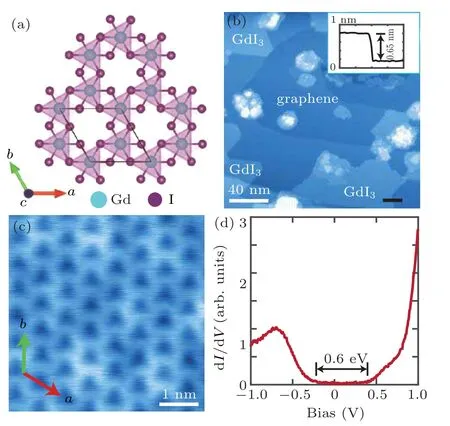
Fig.3. (a)Top view of GdI3 lattice. (b)STM topography(200 nm×200 nm;bias: 3 V; current: 20 pA) of GdI3 films. Inset shows the height profile along the black line when the sample bias is 2.0 V. (c) STM atomic resolution (10 nm×10 nm; bias: 1 V; current: 100 pA) of GdI3. Inset shows the honeycomb lattice of monolayer GdI3. (d) STS of monolayer GdI3 (bias:1.0 V;current: 100 pA).
Finally, we try the growth of CrI2thin flim. A single layer of CrI2consists of one layer of Cr sandwiched between two layers of I atoms. The bulk crystal has two confgiurations. One is similar to that of the 1T-transition metal dichalcogenides but elongated along the b axis (Fig.4(a)).It belongs to the monoclinic crystal structure with the lattice constants of a = 7.545 ˚A, b = 3.929 ˚A, c = 7.505 ˚A,α = γ = 90◦, β = 115.52◦.[21]The inversion symmetry is preserved within single layer CrI2. Another one (Fig.4(b))is orthorhombic with the lattice constants of a = 7.560 ˚A,b = 3.915 ˚A, c = 13.553 ˚A, α = β = γ = 90◦, which breaks the inversion symmetry within single layer CrI2.[22]In both structures, a Cr atom is surrounded by six nearestneighboring iodine atoms. In the thin film growth, Cr (at 1000◦C) and I2released from CrI3(at 208◦C) were codeposited on graphitized SiC (300◦C) for 40 min. Figure 4(c) shows the STM topography of the monolayer film(surrounded by the yellow line). The coverage of the film is lower than one. The apparent height of the film is 7.0 ˚A(see inset of Fig.4(c)) when the sample bias is set at 2.0 V. The atomic resolution image(Fig.4(d))reveals the single I atoms on the topmost layer. The lattice constants are a=7.46 ˚A,b=3.91 ˚A,slightly different from the bulk ones due to unidentified origin. The two different crystal configurations cannot be distinguished by the STM image because of their small difference in the lattice constants. The STS(Fig.4(e))shows that CrI2monolayer is an insulator with bandgap of about 3.0 eV.

Fig.4. (a)Top and side views of CrI2 crystal.[21] (b)Top and side views of CrI2 from Ref.[22]. (c)STM topography(200 nm×200 nm;bias: 4 V;current: 20 pA)of CrI2 films. Edge of CrI2 film is highlighted by yellow line.Inset shows height profile along the black line when sample bias is 2.0 V.(d)STM atomic resolution(10 nm×10 nm;bias: 0.4 V;current: 100 pA)of CrI2. (e)STS of monolayer CrI2 (bias: 1 V;current: 100 pA).
In conclusion, we demonstrate a reliable growth method of iodides by MBE.The thermally decomposed CrI3releases very pure I2vapor, whose flux can be well controlled by the heating temperature. The effectiveness of the iodine source is demonstrated by the growth of MnI2, GdI3, and CrI2thin films. It is expected to promote the study on magnetism at the 2D limit.
猜你喜欢
大众文艺(2022年22期)2022-12-01 11:52:58
Plasma Science and Technology(2022年11期)2022-11-17 03:00:08
Chinese Physics B(2022年8期)2022-08-31 09:59:42
科学导报·学术(2020年86期)2020-11-04 06:41:34
快乐作文·低年级(2017年12期)2017-12-28 16:13:02
校园英语·中旬(2017年13期)2017-12-19 18:59:50
艺术家(2017年2期)2017-11-26 21:26:20
数学学习与研究(2017年2期)2017-03-06 08:12:54
校园英语·下旬(2016年2期)2016-03-18 16:48:21
好孩子画报(2015年1期)2015-06-19 18:12:41

- Chinese Physics B的其它文章
- Statistical potentials for 3D structure evaluation:From proteins to RNAs∗
- Identification of denatured and normal biological tissues based on compressed sensing and refined composite multi-scale fuzzy entropy during high intensity focused ultrasound treatment∗
- Folding nucleus and unfolding dynamics of protein 2GB1∗
- Quantitative coherence analysis of dual phase grating x-ray interferometry with source grating∗
- An electromagnetic view of relay time in propagation of neural signals∗
- Negative photoconductivity in low-dimensional materials∗