
A large-grain-size thick-film polycrystalline diamond detector for x-ray detection
2020-12-02 08:11:16PingXU许平YiYU余羿HaiyangZHOU周海洋andChangjunQIU邱长军
Plasma Science and Technology 2020年12期
关键词:海洋
Ping XU (许平), Yi YU (余羿), Haiyang ZHOU (周海洋) and Changjun QIU (邱长军)
1 School of Resources Environment and Safety Engineering,University of South China,Hengyang 421001,People’s Republic of China
2 School of Physics, University of Science and Technology of China, Hefei 230026, People’s Republic of China
3 School of Mechanical Engineering, University of South China, Hengyang 421001, People’s Republic of China
Abstract
Keywords: polycrystalline diamond film, x-ray detector, electron-assisted chemical vapor deposition
1.Introduction
Since the first finding of the x-ray in 1895,x-ray detection has long been an important issue in scientific research.There are many different x-ray detectors,and the underlying physics of all of these detectors is the interaction between x-ray and materials, such as metal (such as aluminum) in x-ray diodes[1], silicon in silicon diodes, luminescent materials (such as anthracene)in scintillators[2]and gas(such as Xenon)in gas radiation ionization detectors.The photoconductive detector[3] is a kind of x-ray detector based on electric-field-induced directional movement of electron-hole pairs, which are generated in materials after x-ray absorption.Different to other semiconductor photoconductive materials such as InP:Fe and GaAs:Cr, diamond is an insulator photoconductive material and has the best chemical and physical properties.It is suitable to develop detectors not only for x-ray, but γ-ray [4]or neutron [5] detection.Natural diamond is rare and expensive.There are two methods to synthesize diamonds,i.e.the high-pressure high-temperature method [6, 7] and chemical vapor deposition(CVD)[8].As a result of the rapid development of the CVD technique in the 1990s, great progress was made with diamond detectors.
There are two different synthetic diamonds, i.e.polycrystalline diamonds and single-crystal diamonds.On the one hand, without defects in the grain boundary, a single-crystal diamond can reach a collecting efficiency of nearly 100%,while a polycrystalline diamond only has an efficiency in the order of several percent[9].On the other hand,it is difficult to fabricate a high-quality single-crystal diamond and the price is about 30 times higher than that of a polycrystalline diamond [9].This limits the usage of diamond detectors.Apolycrystalline diamond with large grain size means fewer defects than a diamond with small grain size and it should have better electric performance,but surprisingly,few related works have been reported.

Table 1.Comparison between 2theta and intensities of measured diamond spectrum by XRD and the standard diamond spectrum.
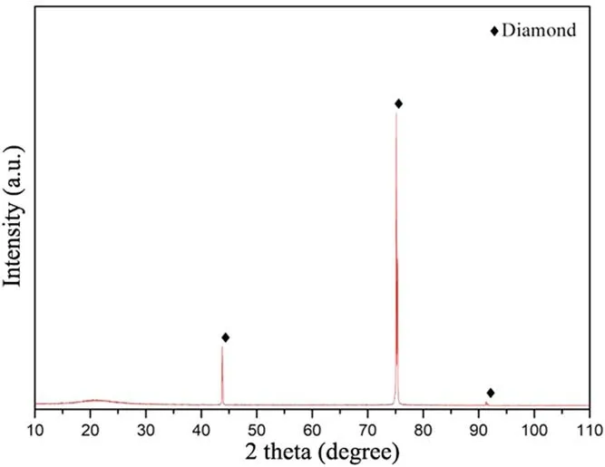
Figure 1.Intensity peaks of this diamond film measured by XRD.
In this article, we present a diamond x-ray detector,which is based on the large-grain-size polycrystalline diamond film.The performance of this diamond detector is discussed and the first experimental results of x-ray detection on a Z-pinch confirm its x-ray detection ability.
2.Diamond film fabrication
The diamond film that is used as the main component in the x-ray detector presented in this article is fabricated in an electron-assisted chemical vapor deposition (EACVD)device.The setup and main parameters of this EACVD device can be found in [10].In this diamond deposition experiment,the working temperature of the tantalum wires is about 2100°C,the temperature of the substrate is about 825°C,the gas flow rate is 100 sccm,the working gas pressure is 4000 Pa and the volume ratio between methane and hydrogen is 1.5:100.After a deposition period of tens of hours,a diamond film 6×6×0.5 mm3is fabricated.

Figure 2.Image of the morphology of the diamond film surface taken by an SEM.
The purity of the diamond can be confirmed by means of checking its Raman spectrum at 1332 cm−1[10, 11] or x-ray diffraction (XRD) spectrum.The measured XRD spectrum is shown in figure 1.One can clearly see two pronounced peaks at 43.628° and 74.650°, which characterize the (111) and(220) surfaces of the diamond, respectively.Another small peak at 90.848° can also be found, which characterizes the(311) surface.Other peaks, which characterize unwanted carbon phase such as graphite,are not found in this spectrum,which indicates the high purity of this deposited diamond.These three angles are slightly smaller than those in the standard diamond spectrum (Diamond, 06-0675), which is due to the locating of the film because the film surface is located slightly lower than the sample plate in this XRD experiment.The comparison between measured and standard spectra is shown in table 1.Except for the slight peak-angle deviation, the peak intensities differ from the standard spectrum.This difference probably comes from the large grain size of the film.The large-size grains mean that fewer grains participate in the diffraction, which leads to weaker intensity and enhanced preferential orientation.For an x-ray detector based on diamond, the size of the crystal grains is very important for its performance.Known as the polarization effect [9], the electrons and holes in the diamond will be trapped in crystal defects, resulting in a space-charge redistribution.Crystal boundary is the main defect in polycrystalline diamonds.A larger grain size implies fewer crystal boundaries and it has been proved that it is beneficial to the production of a much better detector[12,13].To confirm the grain size of this diamond film, a scanning electron microscope (SEM) is used to investigate the morphology of the diamond film surface.Figure 2 shows the image with a scale of 303 μm at its bottom.Like the exposed part of an iceberg,only a small part of the crystal grain is photographed.The real grain size is obviously much larger than hundreds of μm,which indicates fewer crystal boundaries and defects.
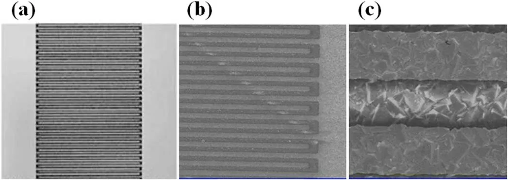
Figure 3.SEM images of the interlaced-finger electrodes with different magnifications.
3.X-ray detector fabrication
After the diamond film is separated from the substrate, both sides of the film are polished, which can greatly enhance the electric performance of the diamond film.The polishing of the deposition side (denoted as ‘side 1’ for convenience) is to make the surface even and get rid of the deposited impurities to increase its resistivity.This process can effectively improve the quality of electrode imprinting and will be discussed later.The polishing of the other side (side 2) is to get rid of the nucleation layer.
High resistivity of a diamond contributes to the high sensitivity and signal-to-noise ratio of a diamond detector.Before resistivity testing, this diamond film is oxidation treated in a boiling sulfuric and nitric acid mixture.The aim of this treatment is to get rid of residual surface graphite and hydrogen atoms,which are linked to the surface carbon atoms during deposition [14].Direct voltage is applied onto this diamond film and a high-sensitive galvanometer is used to measure the current flowing through the film.The resistance is calculated according to Ohm’s law and the resistivity is then derived, taking the size and shape of the film into account.In this experiment,a 10 V biasing voltage is applied and the current is lower than 0.1 pA, which is beyond of the sensitivity of the galvanometer.A resistivity of higher than 1012Ω·cm can be derived.
Metallization is a key procedure in x-ray detector fabrication.Interlaced-finger electrodes are designed and imprinted onto side 1.The SEM images with different magnifications are shown in figures 3(a)-(c).The electrode material is gold.The imprinted range of interlaced fingers is 6 mm×1.9 mm (figure 3(a)).The thickness is 0.8 μm.As mentioned before, polishing improves the imprinting quality because a rough surface will probably increase the risk of defects such as bifurcation, fracture or connection between nearby fingers.This electrode pair is locally zoomed-in, as shown in figures 3(b)and(c),and one can clearly see the high quality of imprinted fingers without obvious defects.Both the gap width between neighboring fingers and the width of one finger are 25 μm.There is a total of 60 finger pairs and figure 3(a) shows half of them.This design ensures a narrow enough gap, which is beneficial to the collection of electric carriers and an effective collection area of 50%.
Annealing at 450°C is applied to the gold electrodes to form the ohmic contact between the diamond film and electrodes.Then, the diamond film is located inside an open-end hollow cylinder,as shown in figures 4(a)-(c),working as the main detection component of the x-ray detector.The cylinder is made of pure copper with gold coating.The size of this cylinder is Ф30 mm×48 mm.Side 1 faces the open end and x-ray in the detection experiments.A gold gasket, which is fixed by four screws, is used to compress the diamond film and silver/epoxy resin is used as an adhesive to ensure the electric contact between the gaskets and one interlaced-finger electrode.The other electrode is connected to the core wire of a Small A Type (SMA) electrical connector (figures 4(a) and(c)).A plastic cover (figure 4(b)), which is transparent to x-ray,is used to protect the diamond film and electrodes from getting dirty.
In figure 5,the experimentally measured current-voltage(I-V) curve of this diamond detector is indicated by black squares.The red line is the linear fit.All data are measured without any ionization radiation,which means that the current in figure 4 is dark current.It is clear that the experimental data show good linearity and symmetry to the coordinate origin.This linearity and symmetry experimentally confirm the ohmic contact.From this figure, it can be concluded that when an electric field of 30 kV cm−1is applied between the electrodes, the dark current of the detector is lower than 0.1 nA.This dark current is slightly better than that of the natural IIa diamond detector, which has a dark current in the order of 0.1 nA at an electric field of 14 kV cm−1.
A femtosecond dye laser is used to test the time response of this diamond x-ray detector, which is an important parameter for applications of short-pulsed x-ray detection.The experimental setup of the time response testing is shown in figure 6.The wavelength of the laser is 365 nm.The biasing voltage applied between the two electrodes is 100 V.The output of the oscilloscope is shown in figure 7.The time period of 10%-90% amplitude is 235 ps.Because the rise time of the laser is 15 ps, the rise time of the signal is about 220 ps.

Figure 4.Diamond detector images.(a) Side view, (b) bottom view (two detectors), (c) top view.

Figure 5.Experimentally measured current-voltage(I-V)data of the diamond detector(black squares)and linear fit of I-V data(red line).
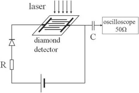
Figure 6.Experimental setup of the time response test of the diamond detector.
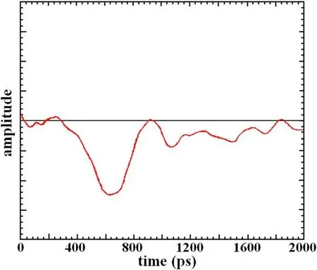
Figure 7.Output of the diamond detector in the time response test experiment.
The sensitivity of this diamond detector is calibrated by a traditional xenon-filled flat ionization chamber (model DLS-504).The experimental setup is shown in figure 8.An x-ray with an energy of 15 keV is used as the radiation source.A highsensitive galvanometer is used to measure the output of the ionization chamber and diamond detector with (Iion,w,Idia,w) or without (Iion,w/o,Idia,w/o) x-ray radiation to cancel out the background currentIion=Iion,w−Iion,w/oandIdia=Idia,w−Idia,w/o.Then,the sensitivity of the diamond detectorSdiacan be derived from the sensitivity of the ionization chamberSion=4.36 ×10⁻²A W−1by,

whereAion= 4 ×4 mm2andAdia= 6 × 1.9 mm2×50%stand for the effective detection areas of the ionization chamber and diamond detector, respectively.The biasing voltage of theionization chamber is 1000 V.Two biasing voltages,i.e.50 and 100 V are applied onto the diamond detector.The measured sensitivity of the diamond detector is listed in table 2.
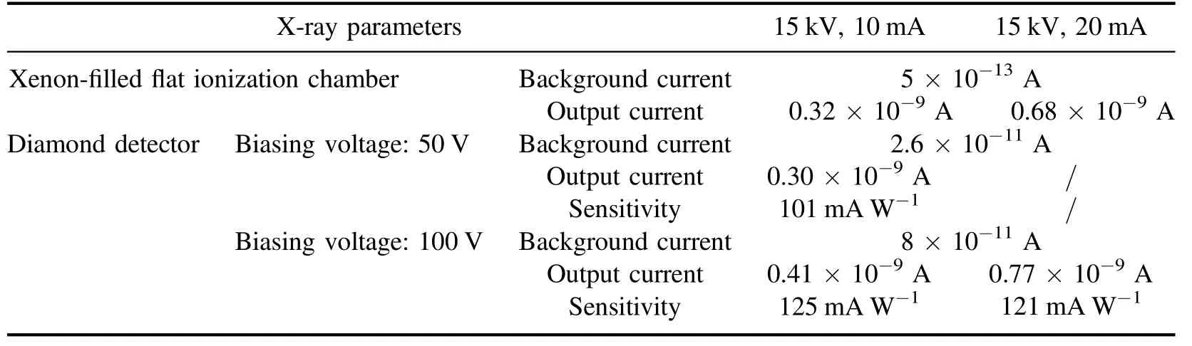
Table 2.Experimental parameters and measured sensitivity of the diamond detector.
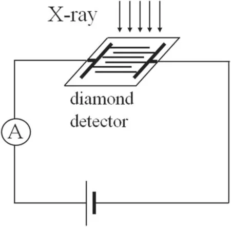
Figure 8.Experimental setup of the sensitivity test of the diamond detector.
Keeping the parameters of the x-ray(15 kV,10 mA),the sensitivity of the diamond detector increases from 101 to 125 mA W−1as the biasing voltage increases (from 50 to 100 V).The reason lies in the increase of migration speed of carriers, which benefits collection efficiency.Keeping the voltage of the x-ray source and changing the current from 10 to 20 mA, the output of the diamond detector almost doubles(from 0.41×10⁻⁹A to 0.77×10⁻⁹A),which results in an almost unchanged sensitivity (from 125 to 121 mA W−1).This indicates a fairly good linear radiation dose rate of the detector.
4.First result of x-ray detection

Figure 9.Evolution waveform of x-ray intensity measured by the diamond detector in the Z-pinch experiment.
This diamond detector now works as one of the main x-ray detectors on a Z-pinch.Foam is located at the center of the pinch.A double-layer ‘nested tungsten wire array’ is distributed evenly around the foam.There are 120 tungsten wires in the inner layer and 240 wires in the outer layer.When a total current, which is in the order of mega-amperes, is led through these wires in nanoseconds, double-layer tungsten plasma will form and a strong x-ray will be irradiated during the strong collisions between the layers and the foam.The physics of Z-pinch is complicated and beyond the scope of this article.The dynamics of wire ablation and x-ray production on Z-pinches can be found in[15,16]and the physics on double-layer tungsten wire array can be found in[17,18].
The evolution waveform of x-ray intensity measured by this diamond detector is shown in figure 9.A pronounced peak, which characterizes the strong collision between tungsten plasma and the foam, can be found with a full width at half maximum of about 5.8 ns.This is a typical time scale of x-ray burst [15-17] on similar Z-pinch devices, which is measured by traditional x-ray diodes.It is to be noted here that about 31 ns before this main peak,there is another small peak, which characterizes the x-ray burst caused by the collision between the inner tungsten plasma layer and outer one.
5.Discussion and summary
6×6×0.5 mm3diamond films have been fabricated using the EACVD method.Discrete peaks in the XRD spectrum and the pronounced clean peak at 1332 cm−1in the Raman spectrum confirm the high purity of diamond phase in the deposited diamond film.The intensity deviations of the peaks in the XRD spectrum and SEM images confirm the large grain size of the film, which is much larger than hundreds of μm.This large grain size means fewer grain boundaries in the film, which is the main weakness of polycrystalline diamond compared to single-crystal diamond.
An x-ray detector has been fabricated using this thick diamond film.Interlaced-finger electrodes are imprinted on the film.The gap is 25 μm between neighboring fingers.It is to be noted that the gap width is much smaller than the grain size.This is very important in the detector design, which means carriers such as electrons and holes can be collected by the electrodes without passing through the grain boundaries.
The I-V curve has been experimentally measured.The linearity and symmetry to the coordinate origin confirm ohmic contact of the electrodes.The dark current is lower than 0.1 nA when an electric field of 30 kV cm−1is applied between the electrodes.This dark current is better than those of the natural IIa diamond detectors and other reported polycrystalline diamond detectors [14, 19-21].The time response of about 220 ps is experimentally measured by a femtosecond dye laser,which is close to that of the natural IIa diamond detectors (about 100 ps).One of the advantages of synthetic polycrystalline diamond detectors is that the electric performance can be optimized by controlling the deposition parameters.After optimization of the diamond time response,it proved to be better than 100 ps [20].In the application of x-ray detection presented in this article,the time scale of x-ray evolution is tens of nanoseconds and a time response of 220 ps is sufficient.
With a biasing voltage of 100 V, the sensitivity of the diamond detector is about 125 mA W−1.This sensitivity is one order of magnitude higher than reported works, such as 2.2 mA W−1in[14].As discussed above,this high sensitivity is attributed not only to the large grain size, but the narrow gap between neighboring fingers.Decreasing the gap width benefits carrier collecting, resulting in a higher sensitivity.This sensitivity approaches the excellent sensitivity of silicon photodiodes,which is about 200 mA W−1[22],although it is still lower, which is determined by the larger band gap of diamond compared to silicon.A good linear radiation dose rate is also confirmed, which implies that the diamond detector can not only work for x-ray detection in Z-pinches,but is a good candidate for dose measurement in medical practice.
It is meaningful to compare the performance of the diamond detector to other traditional x-ray detectors.Among these detectors, the x-ray diode is the most commonly used.First of all, without considering the electrical performance in x-ray detection, diamond detectors have a much wider application range and much higher reliability because of their excellent physical and chemical properties.For example, the x-ray diode does not work in a high-temperature environment because the metal (such as aluminum) electron emissivity changes along with temperature and it does not work in a highly corrosive environment because the metal will be corroded.Conversely, it has been proved that diamond detectors have the ability of to work in these harsh environments [23-25].The chemical property of aluminum cathode in x-ray diodes is unstable and the sensitivity will drop a lot after a long time period of non-use.So x-ray diodes need recalibration every time before usage.Another important characteristic of an x-ray diamond detector is its wide detection energy range.The x-ray diode can only detect x-ray in a relatively lower energy range, for example hundreds of eV.When the x-ray energy is higher (such as 1.5 keV), its sensitivity decreases sharply.For a diamond x-ray detector,the sensitivity does not decrease much, but increases somewhat as the x-ray energy increases.
The electrical performance of the diamond detector is also compared with x-ray diodes.The dark current of the diamond detector is 2.6×10⁻¹¹A (50 V biasing, table 2)and the typical dark currents of x-ray diodes are 10−13A.For x-ray detection in Z-pinch, whose output is in the order of 10−9A, both kinds of detectors are acceptable, but for ultralow-dose x-ray detection x-ray diodes are better.The time response of the diamond detector is about 200 ps and that of an x-ray diode is lower than 100 ps.The sensitivity of the diamond detector is in the order of 100 mA W−1, which is comparable to that of an x-ray diode.
In summary, a kind of x-ray detector based on thick synthetic polycrystalline diamond film is presented.High electrical performance, which is attributed to the high purity of diamond phase, large grain size and narrow gap width between fingers,has been experimentally confirmed.The test on a Z-pinch,which has a double-layer‘nested tungsten wire array’ indicates the x-ray detection ability of this diamond detector.
Acknowledgments
This work is supported by the National Key R&D Program of China (Grant No.2017YFE0301300) and the Hunan Provincial Innovation Foundation for Postgraduate (Grant No.CX2018B588).
猜你喜欢
红领巾·萌芽(2022年10期)2022-11-24 06:03:06
金桥(2022年8期)2022-08-24 01:33:30
百科探秘·海底世界(2021年9期)2021-10-11 10:41:03
少年漫画(艺术创想)(2019年9期)2020-01-18 08:38:04
心声歌刊(2019年3期)2019-06-06 02:52:32
当代音乐(2018年4期)2018-05-14 06:47:13
金色少年(奇趣科普)(2017年12期)2017-12-26 06:22:45
琴童(2017年7期)2017-07-31 18:33:48
小学科学(2017年5期)2017-05-26 18:25:53
红领巾·萌芽(2016年1期)2016-09-10 07:22:44
 Plasma Science and Technology2020年12期
- Plasma Science and Technology的其它文章
- In vitro study of nonthermal atmospheric pressure plasma in improving the durability of the dentin-adhesive interface with an etch-and-rinse system
- The dynamics of a nanosecond gas discharge development with an extended slot cathode in argon
- Coupling model of AC filter branch in SF6 circuit breaker during the break process
- Molecular dynamics simulations of the interaction between OH radicals in plasma with poly-β-1-6-N-acetylglucosamine
- New method for rekindling the explosive waves in Maxwellian space plasmas
- Mitigation of blackout problem for reentry vehicle in traveling magnetic field with induced current