Femtosecond laser processing of lithium niobate crystal:principle and applications
Zhou Chao,Ma Jia-Nan,Xu Xiao-Yi,Xu Chuan,Zhang Yong*,Zhu Shi-Ning,Xiao Min,2
1.National Laboratory of Solid State Microstructures,College of Engineering and Applied Sciences,and School of Physics,Nanjing University,Nanjing 210093,China
2.Department of Physics,University of Arkansas,Fayetteville,Arkansas 72701,USA
Abstract:Femtosecond(fs)-laser micromachining is an effective material processing method because of its ultrashort pulse width and extremely high peak intensity.Fs-laser micromachining technology has been widely used to process photonic integrated devices.Lithium niobate(LN)crystal is a common material in integrated and guided-wave optics because of its excellent electro-optic,nonlinear optical,and piezoelectric properties.This review describes fs-laser processing of LN crystal,mainly focusing on the physical principle of fs-laser processing and the recent advances of LN-based photonic devices.Fs-laser technology makes LN crystal a promising platform in the field of micro-nano photonics.
Key words:femtosecond laser;lithium niobate;waveguides;nonlinear photonic crystals;laser processing
CONTENTS
V.Conclusion 81
Acknowledgments 81
References 81
I.Introduction 69
II.Mechanisms of fs-laser processing in LN crystals 70
A.Ultrafast laser-induced damage in LN crystal 71
1.Surface ablation 71
2.Microexplosions 72
B.Refractive index changes induced by fs-laser
irradiation 72
C.Spot distortion and aberration compensation
technology in LN 73
III.LN-based photonic devices processed by an fs laser 74
A.LN-based waveguide structures 74
1.Type-I waveguides 75
2.Type-II waveguides 75
3.Type-III waveguides 76
B.Photonic devices based on waveguide structures 76
1.Integrated LN electro-optic modulators 76
2.Frequency converters in LN waveguides 76
C.Photonic crystals 77
D.High-Q-factor LN-based microresonators 78
IV.LN nonlinear photonic crystals 78
I.INTRODUCTION
Femtosecond(fs)lasers have become a powerful tool for processing materials since their first demonstration in 1994[1].Compared with other fabrication technologies,fs-laser micromachining has some unique advantages.First,the ultrashort pulse width of fs lasers can strongly suppress thermal diffusion and the formation of heat-affected zones.Therefore,fs-laser processing can achieve sub-diffraction-limit resolution(i.e.,ultrahigh precision)in transparent materials.Second,when a fs laser beam is tightly focused inside a transparent material,the fs laser-induced nonlinear interactions are confined to the focus volume,resulting in internal modification in this specific region[2].Thus,fs-laser processing is a truly three-dimensional(3D)micromachining technique,which can be used to fabricate complex structures.Third,fs-laser processing is highly fl exible,which means that it can be adapted to treat different substrates by choosing suitable irradiation parameters including wavelength,pulse energy,pulse duration,repetition rate,focusing conditions,and rate[3].Additionally,different processing parameters may result in different phase and structural modi fications of substrates[4].

FIG.1.Schematic diagram of the interaction physics between fs laser pulses and a transparent material.(a)The laser is focused into the bulk transparent sample.(b)The energy is nonlinearly absorbed via multiphoton,tunneling,and avalanche photoionization and free-electron plasma is generated.(c)The hot electron–ion plasma transfers its energy to the lattice of the sample on a time scale of~10 ps,which induces permanent structural modification.(d)Three types of permanent modification have been identified:isotropic refractive index changes at low pulse energy,sub-wavelength birefringent nanostructures at moderate energy,and empty voids at high pulse energy.
Lithium niobate(LN)crystal is a widely used dielectric material in photonics because of its excellent electro-optic(EO),piezoelectric,and nonlinear optical properties[5]. LN crystal is commonly used in high-speed light modulation[6-11],nonlinear processing[12,13],waveguide structures[14,15].In this review,we mainly focus on the fs-laser micromachining of LN crystal.In Section II,we brie fl y introduce the physical mechanisms of the interaction between an fs laser pulse and LN crystal.Section III presents LN-based optical waveguides and other photonic devices fabricated by fs-laser micromachining.In Section IV,we review the recent development of LN nonlinear photonic crystals(NPCs)through fs-laser domain engineering technique.Finally,we discuss future perspectives of fs-laser micromachining in LN photonic devices.
II.MECHANISMS OF FS-LASER PROCESSING IN LN CRYSTALS
The high peak intensities produced by a focused fs laser leads to strong nonlinear absorption in LN crystal.Several picoseconds later,the laser-excited electrons transfer their energy to the LN lattice,which causes the properties of LN crystals to change[3].Although the physical mechanisms of material modification after the electrons transfer their energy to the LN lattice still perplex researchers,three types of morphologies have been obtained at different laser energy levels[16],as shown in Fig.1.
According to the laser intensity irradiated on a dielectric material,the fs laser-induced changes are divided into two categories:damage and modification.Here,damage indicates the irreversible structural changes caused by high laser intensity over the damage threshold,and includes surface breakdown,microexplosioninduced voids,and so on.The damage induced at high laser energy can be explained using the ther-mal diffusion model. The second category of laserinduced modification is the non-destructive reversible phase transitions caused by low laser intensity near the damage threshold such as a change of refractive index(by~10-3).Laser-induced modifications include stress changes,thermal effects,and alteration of material properties like bandgap and thermal conductivity.Additionally,fs-laser pulses can also lower the crystallinity of domains[12]and invert the ferroelectric domains[17]of LN crystal,which creates a new path to fabricate nonlinear photonic devices.
A.Ultrafast laser-induced damage in LN crystal
1.Surface ablation
Focusing an fs laser on or near the surface of an LN crystal will cause ablation of the crystal surface.There are two main types of fs-laser pulsed laser ablation:nonthermal ablation using a laser f l uence near the damage threshold[18]and thermal ablation when the laser f l uence is above the damage threshold.As an example of nonthermal ablation,in 2007,Yu et al.[19]observed laser-induced periodic surface structures,also termed periodic ripples,with a period of 200 nm on the bottom surfaces of ablation spots in LN crystal.Fig.2 shows scanning electron microscopy(SEM)images of the sub-wavelength ablated spots formed at different multipulse energies and repetition frequencies.These sub-diffraction limit structures may be formed by multiphoton excitation.
There are many factors that can inf l uence the surface damage threshold of a material,such as the pulse number,laser energy,and impurity doping.Chen et al.[20]demonstrated experimentally that the surface ablation threshold decreased substantially with the increase of the pulse number applied to a surface until reaching an almost constant level.In addition,the damage depth can be controlled by the number of pulses and laser energy[21].

FIG.2.SEM images of the surface topography of an LN crystal after ablation with an fs laser with different pulse energies and numbers of(a)470 nJ,1000 pulses,(b)100 nJ,1000 pulses,(c)60 nJ,1000 pulses,(d)50 nJ,1000 pulses,(e)100 nJ,4 pulses,(f)100 nJ,16 pulses,(g)60 nJ,31 pulses,and(h)50 nJ,62 pulses.(Reprinted with permission from[19].©2008 IOP Publishing Ltd.)
Many experimental studies[22-25]have been performed to predict the damage threshold of LN crystals.Su et al.[25]presented a detailed explanation of the interaction between an fs laser pulse and LN crystal based on the classical two-temperature model[26].When a region inside an LN crystal is irradiated by an fs laser pulse,a huge number of carriers are generated by multiphoton and avalanche ionization in an ultrashort duration.The carriers absorb the photon energy and their temperature rises sharply.In such a short duration,the energy cannot be transferred to the LN lattice but is instead transferred to electrons,which increases the electron temperature.At the end of the pulse,the electrons transfer energy to the lattice.As a consequence,the electron temperature drops and the lattice temperature rises until they reach thermal equilibrium.If the thermal equilibrium temperature is higher than the melting point of the LN crystal,irreversible damage will be caused by melting.This physical process can be described mathematically as follows:

where Ceand Clrepresent the heat capacity of electrons and the lattice system,respectively; κeand κlare the heat conductivity of electrons and the lattice,respectively;Teand Tlrepresent electron temperature and lattice temperature,respectively;φ(Te-Tl)is the energy dissipation per unit time per unit volume in the electron system;and S is the laser source term.These equations provide an effective numerical way to predict the surface ablation threshold and analyze the variations of damage threshold of crystals with fs-laser parameters[25].
2.Microexplosions
When a tightly focused fs-laser beam is incident to the bulk of LN,multiphoton absorption produces highly localized plasma.Rapidly diffusing plasma can trigger microexplosions that eject the material from the focal point,forming voids inside the crystal[27].Fig.3 depicts images of void formation.Fs-laser-induced microexplosions have been exploited to fabricate photonic crystals(PCs)in many transparent materials,including LN crystal.However,LN crystal is a birefringent crystal with high refractive index,so the light focus is distorted[27-29]during micromachining processes(see Section II.C for details).
The abovementioned types of micromachining mainly involve the destructive processing of LN crystal.However,the principle of the interaction of fs-laser pulses with materials is still not understood completely and further theoretical and experimental research on this topic is needed.In the following part,we discuss the internal modification of LN crystal.
B.Refractive index changes induced by fs-laser irradiation
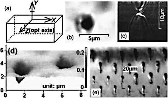
FIG.3.Illustrations of void formation after microexplosions.(a)Schematic of the directions of the LN sample and laser polarization.(b)Confocal transmission image and(c)depth scanning confocal ref l ection image of a single void.(d)Atomic force microscopy image of voids.(e)Cross-sectional confocal transmission image of voids fabricated at various depths with the same power.(Reprinted with permission from[27].©2005 American Institute of Physics.)
In 2004,Gui et al.[30]observed an extraordinary refractive index change of LN crystal when the laser intensity was lower than the damage threshold.After that,Burghoff’s group[31]investigated the origin of this modification in detail.They considered the photorefractive effect,migration of ions,and defects in the crystalline lattice.In the photorefractive effect,free electrons generated by nonlinear ionization move along the crystal axis because of their inhomogeneous distribution.Then the inhomogeneous distributions change the refractive index via the electro-optic effect[31,32].In ion-implanted LN crystal,inhomogeneous ion distributions cause ion migration.Thus,the diffusion of lithium ions can also explain the change of refractive index induced in the LN crystal[33].In 2010,Gamaly et al.[34]investigated the inf l uence of pulse parameters on the change of refractive index,which demonstrated that the number density of excited electrons induced by fs laser was two orders of magnitude higher than that produced by a long-pulse laser.However,it has been found that the refractive index changes induced by fs lasers are not stable at high temperatures[14],which limits their application scope.Additionally,fs-laser-induced damage also generates a stress field and increases the refractive index of the sample around the focus spot[35].It is worth noting that this refractive index change does not affect the lattice structure significantly,which greatly facilitates the processing of LN-based optical devices.This feature has been widely used in waveguide fabrication[36].
If the LN lattice is not destroyed during laser processing,then its nonlinear optical properties can be preserved[37].Conversely,when the fs-laser power is too high,the material properties of the light guide area will change[37,38].This feature can also be used to manufacture nonlinear photonic devices[12,39-41].
C.Spot distortion and aberration compensation technology in LN
When a focused laser wavefront is incident through the interface of two media with different refractive indices,spherical aberration occurs,which distorts the focal spot.The larger the refractive index difference,the stronger the spherical aberration.For LN crystal,which has a refractive index of~2.25 at 800 nm,this distortion will be more serious compared with that of other standard materials such as glass,which has a refractive index of~1.5.In addition,LN crystals show uniaxial birefringence,and even though the birefringence of LN is weak,this additional aberration will still result in splitting of the focus during direct laser writing[42].
In 3D direct laser writing,a laser beam usually passes through an objective lens and is focused inside a transparent material.Generally,the focal spot distribution tends to be elongated in the axial direction,which limits the resolution of processing.Several approaches have been proposed to solve this problem,such as slit-beam shaping[43]and phase compensation by a deformable mirror[44,45]or spatial light modulator[46].In 2011,Simmonds et al.[47]used both a deformable mirror and spatial light modulator to correct the extreme spherical aberrations generated when using lenses with high numerical aperture(Fig.4).Another technology to improve beam focus is spatiotemporal focusing,which was first demonstrated in 2010[48].This approach can largely avoid nonlinear self-focusing before the focus,particularly in highly nonlinear materials such as polymers and crystals.
For isotropic materials,the light distribution close to the focus can be expressed as:


FIG.4.Experimental setup using a dual adaptive optics system.(Reprinted with permission from[47].©The Optical Society.)

FIG.5.Numerical intensity distribution of a laser focused at depths of 0,7.5,and 15 μm in LN without any compensation.(Reprinted with permission from[28].©The Optical Society.)
where θ1and θ2are the angles of the light beam of convergence outside and inside the material,respectively;τsand τpare the Fresnel transmission coefficients for the s-and p-polarization states,respectively;J0is the zero-order Bessel function;and α is the maximum angle of the incident light ray.The phase delay Φ through the plane of the material is expressed as:

where k is the wavenumber given by 2π/λ.Fig.5 shows the numerically calculated focus intensity distribution,which indicates that the phase mismatch could cause both defocusing and spherical aberration[28].
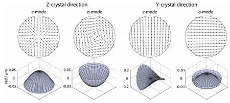
FIG.6.Polarization eigenmodes(top row)and corresponding aberration functions of the per micron focusing depth(bottom row)for the(a)Z-crystal direction and(b)Y-crystal direction in an LN crystal.(Reprinted with permission from[42].©The Optical Society.)
For LN crystals,the situation would be more complicated because of its uniaxial birefringence.Stallinga et al.[49,50]derived the light field distribution in a birefringent crystal under tight focusing.It was found that the aberration functions divided into two polarization eigenmodes under birefringence,as illustrated in Fig.6.In 2009,Zhou et al.[42]observed that when a fs-laser beam was tightly focused into a uniaxial LN crystal along the optical axis,the focal spot split into two sub-peaks.The splitting caused by the different birefringence of the ordinary and extraordinary polarization eigenmodes can lead to the generation of multiple distinct voxels near the focus.The researchers concluded that to fabricate high-quality microstructures,the polarization of the laser should match that of one polarization eigenmode.For LN crystal,to avoid focus splitting,we can orient the crystal in the Y direction with the linearly polarized laser beam along the Z or X direction.If processing along the optical axis is needed,radially or azimuthally polarized light should be used.
III.LN-BASED PHOTONIC DEVICES PROCESSED BY AN FS LASER
LN crystal is regarded as the “silicon of photonics”in recent years[51].Many integrated photonic devices based on LN have been designed and experimentally realized,such as optical waveguides[14],optical modulators[6-9,11],optical frequency converters[37,38,52-54],microresonators[55-59],PCs[60],NPCs[12,61,62],and 3D data storage devices[39,63-66].In this section,we will review LN-based waveguides fabricated by fs laser micromachining and their applications in EO modulators and frequency converters.In addition,PCs and microresonators produced by fs-laser processing of LN substrates will also be introduced.
A.LN-based waveguide structures
A waveguide is an optical transmission structure consisting of a core with a high refractive index surrounded by a cladding with a low refractive index.Waveguides are basic indispensable components of integrated photonics.Although many technologies have been used to fabricate waveguides,such as ion diffusion,proton exchange,and ion exchange[15],it is still a challenge to fabricate complex waveguide structures[30].Fs-laser micromachining is recognized as a highly effi-cient technique for direct 3D processing of transparent materials.
According to the difference of the laser-induced refractive-index change regions,the configuration of waveguides fabricated on LN crystal can be divided into three types(denoted as type I,II,and III)[14].Type-I waveguides are ones in which the refractive index is increased in the processed region and type-II waveguides have an increased refractive index around the processed region.Type-II waveguides are also called double-line waveguides.The double-line method can also be ex-tended to inscribe three or more parallel lines to guide light,which provides type-III waveguides(also called depressed cladding waveguides)[67].In this section,these three different types of waveguides are described in detail.
1.Type-I waveguides
In type-I waveguides,which are also called directly written waveguides,refer to the structures located inside the fs-laser-induced tracks.When the incident ultrashort light f l uence is weaker than the damage threshold,positive refractive index changes in the focal volume can be observed,as mentioned in Section II.Some characteristics of type-I waveguides should be noted.First,only a few materials have been used to fabricate type-I waveguides to date,such as ZnSe[68],Nd:YCOB[69],and LN[30,31,38]crystals.In these crystals,the positive index change only occurs along a specific axis;in other words,this type of waveguide can only guide light with a certain polarization.For zcut LN crystal,the laser irradiation only induces an increase of the extraordinary index[38]. In general,the lattice structure can be preserved when the light intensity is weak[37],but some research has shown that damage could occur as the laser intensity increases[31].Additionally,type-I waveguides are not stable after annealing and the waveguide structure will gradually disappear even at room temperature,which means that it cannot be used under high-power conditions[14].These disadvantages limit the potential applications of type-I waveguides.Nevertheless,type-I waveguides are still useful in many applications.In 2004,Gui et al.[30]produced a type-I waveguide in pure LN crystal;they also demonstrated a Y splitter.In 2006,Lee et al.[38]inscribed waveguide structures in period-poled lithium niobate(PPLN)and demonstrated second harmonic generation(SHG).The conversion efficiency was 6×10⁻³%/W.To suppress the lattice damage,Osellame and colleagues devised a multiscan approach that minimized the single scan energy;the resulting waveguide mode is shown in Fig.7[37].The fabricated waveguides showed high stability.
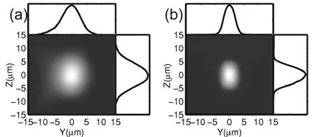
FIG.7.Near-field images of type-I waveguide modes at(a)1567 and(b)783.5 nm.(Reprinted with permission from[37].©2007 American Institute of Physics.)
2.Type-II waveguides
Type-II waveguides are also called stress-induced waveguides and are structures near the fs-laser-induced tracks.When the incident ultrashort light f l uence is higher than the damage threshold,the light will induce lattice damage.The refractive index decreases in the focal volume and increases around the processed region because of the induced stress field[70],as illustrated in Fig.8.If we inscribe two parallel lines close to each other in a crystal,the refractive index of the area between the two lines will increase relative to that of the bulk LN.This method is called the doubleline or dual-line method[14]and the resulted waveguides are called type-II waveguides[36]or stress-induced waveguides.Compared with type-I waveguides,type-II ones have unique advantages[14].First,the fabricated waveguide core and damaged region do not overlap,so the lattice structure is preserved,which is important for some waveguide applications[71,72].Second,this technology can fabricate waveguides in any material and the refractive-index changes are easier to control than in the case of type-I waveguides.Third,type-II waveguides can support the propagation of two orthogonal polarization states.Fourth and most importantly,type-II waveguides are stable at high temperature,which has enabled the fabrication of many high-power waveguide devices.
For LN waveguides fabricated by the double-line method,the measured transmission loss is as low as 1 dB/cm[53],and the luminescence and nonlinear properties of LN are well preserved.Therefore,this method can also realize nonlinear optical processing[52,53,73]or be used to fabricate an integrated EO modulator with embedded electrodes and waveguides by micromachin-ing of PPLN crystal[10].

FIG.8.(a)Microscope image of the end facet of a type-I waveguide,(b)mode field at a wavelength of 1064 nm,and(c)mode field at a wavelength of 532 nm.(Reprinted with permission from[53].©2007 American Institute of Physics.)

FIG.9.(a)Schematic of the fabrication of a depressed cladding waveguide. (b)Optical microscope images of cross sections of LN-based depressed cladding waveguides.(Reprinted with permission from[74].©The Optical Society.)
3.Type-III waveguides
Depressed cladding waveguides possess a core surrounded by several low-refractive-index fs-laser-induced damage tracks. The refractive indices in depressed cladding and type-II waveguides are decreased by fslaser processing and they can share the same processing method.However,the waveguide core of depressed cladding waveguides is located inside the induced low-refractive-index tracks,which is a substantial difference from the structure of type-II waveguides.Thus,depressed cladding waveguides are also classified as type-III waveguides.A depressed cladding waveguide was first realized in ND:YAG crystals[67].He and co-workers fabricated and characterized depressed cladding waveguides in LN crystals by fs-laser processing[74].The experimental setup for waveguide fabrication and microscope images of the waveguide cross sections are provided in Fig.9.Single-mode propagation of light at a wavelength of 4 μm was achieved for a waveguide with a diameter of 50 μm.Theoretically,the cross sections of the fabricated waveguides can be of any shape and support any propagation mode.
B.Photonic devices based on waveguide structures
1.Integrated LN electro-optic modulators
LN is suitable for high-speed EO modulators because of its strong EO(Pockels)effect and fs-timescale response[6,7].Generally,EO modulators are fabricated as Mach–Zehnder interferometers.In 2008,Liao et al.[10]used an fs laser to fabricate Mach–Zehnder interferometer EO devices based on a type-II waveguide on an x-cut LN crystal,realizing an EO modulator along the Y direction.Fig.10 shows a schematic of this modulator.The voltage difference between the adjacent maximum and minimum of optical intensity output was about 19 V and the measured extinction ratio was only ~9.2 dB.Ringleb’s group demonstrated an amplitude modulator for a wavelength of 532 nm with an extinction ratio above 10 dB and half-wave voltage of 23 V[9].In 2012,Horn et al.[11]reported a tunable waveguide Bragg grating in an x-cut LN wafer and demonstrated EO control of the Bragg ref l ection.The external field strength ranged from-22 to 22 V/μm.

FIG.10. Schematic diagram of an LN EO modulator.(Reprinted with permission from[10].©The Optical Society.)
2.Frequency converters in LN waveguides
Waveguides can confine light propagation in specific areas,which can enhance the nonlinear interaction to a certain extent.Currently,LN waveguides processed by fs lasers are widely used in frequency conversion.Based on birefringent phase matching,Burghoffand coworkers realized frequency doubling at 1064 nm in an fs-laser-processed waveguide[54].This type-II waveguide was fabricated in bulk MgO-doped LN crystals and its conversion efficiency was 49%.In the same year,by directly writing type-I waveguides in PPLN,as shown in Fig.11,Lee et al.[38]obtained SHG at 1563 nm.In 2007,Thomas and colleagues described the fabrication of symmetric type-II waveguides in a PPLN z-cut crystal with a conversion efficiency that reached 58%[53].
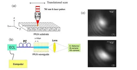
FIG.11.Second-harmonic generation(SHG)in a PPLN waveguide.(a)Schematic of the waveguide writing setup using an fs laser.(b)Experimental setup used to measure the SHG.(c)Near-field mode profiles:(1)fundamental wave(1563.16 nm)and(2)second-harmonic wave(781.58 nm).(Reprinted with permission from[38].©2006 American Institute of Physics)

FIG.12.(a)-(c)Cross-sectional views of voids fabricated in LN.(d)Voids at different depths fabricated near the damage threshold.(e)The 16-1ayer 3D fcc PC.(Reprinted with permission from[29].©The Optical Society.)
C.Photonic crystals
PCs are artificial periodic structures with a photonic bandgap that have attracted extensive interest for use as basic materials in communication technologies.PCs can control light and inhibit light propagation over a spectral region via multiple Bragg diffraction[75].For PCs,it is important to develop methods to produce 3D lattices with a complete photonic bandgap in optical spectral regions.In general,the higher the refractive index contrast between the materials and immersion medium of the objective,the easier it is to open large and complete bandgaps.The requirement of a high refractive index makes LN crystal an ideal candidate material to fabricate PCs.However,the large refractive index mismatch will introduce strong spherical aberration at the focus area.Zhou and Gu[29]investigated the effect of spherical aberration and then fabricated 3D PC-s in LN crystal using the fs-laser-induced microexplosion method.The fabricated voids were quasi-spherical when the main peak of the laser spot had a power slightly above the damage threshold,which allowed the spherical aberration effect to be avoided.They stacked quasi-spherical voids layer by layer and adjusted the laser power to meet the damage threshold for each layer to fabricate a 16-layer 3D face-centered-cubic(fcc)PC in LN.The structure of this PC is shown in Fig.12,and it displayed an obvious bandgap of around 2.2 μm.In 2011,Cumming et al.[28]used a liquid-crystal spatial light modulator to compensate for the extra phase induced by the refractive-index mismatch.They demonstrated that the use of their adaptive compensation method allowed the fabrication depth and stopgap strength in the corresponding PCs to increase by factors of two to three.
D.High-Q-factor LN-based microresonators
Microresonators has an important position in modern photonic applications.Whispering gallery mode(WGM)microresonators with a high-Q factor can confine a light field within an extremely small volume for a long time[76].Thus,WGM microresonators can remarkably increase the strength of a light field and facilitate nonlinear interactions.Fabrication of high-Q LN-based microresonators by material growth and lithography is limited to the millimeter scale[58].Smaller microresonators can be produced by the fs-laser 3D direct writing technique[77],which achieves efficient and high-precision ablation of LN thin films.
Recently,Lin et al.[59]fabricated on-chip high-Q sub-millimeter LN microresonators by fs-laser 3D micromachining.The steps involved in their technique are shown in Fig.13.An LN thin-film sample was formed by bonding an ion-sliced LN thin film onto an LN substrate coated with a sandwiched silica layer[56].An fs laser was used to ablate the LN thin film,which was immersed in water,to form a cylindrical post.After smoothing by focused ion beam(FIB)milling,chemical wet etching by 5%hydrof l uoric acid(HF),and hightemperature annealing,a high-Q freestanding LN microresonator(i.e.,a thin disk on top of a micropedestal)was obtained.This microresonator showed a Q-factor of 2.5×10⁵around 1550 nm.
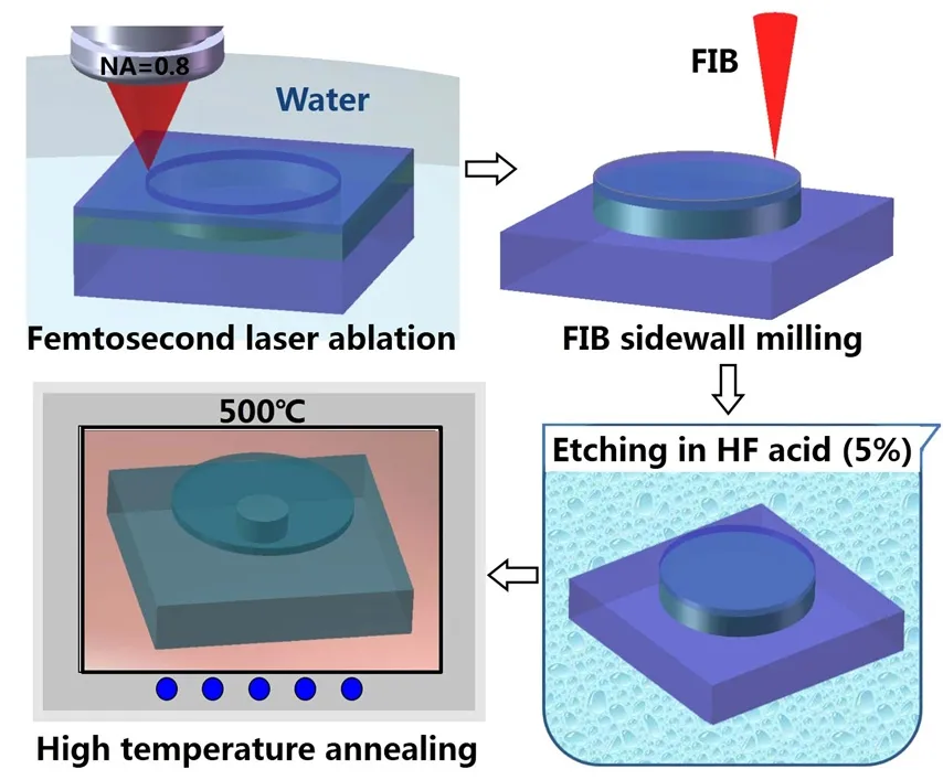
FIG.13.Fabrication of an LN microresonator by waterassisted fs-laser ablation,followed by FIB milling,selective chemical etching with HF,and annealing.(Reprinted from[59]via the Creative Commons Attribution License.©2015,Springer Nature.)
Subsequently,the same group investigated the nonlinear parametric process in high-Q on-chip LN microresonators[55]. It is difficult to simultaneously ensure the phase-matching condition and coherent multiple-resonance condition for all the waves participating in the nonlinear conversion process.They overcame this difficulty by selectively exciting high-order modes in the thin-disk LN microresonator fabricated by fs-laser direct writing.Their results demonstrated that highly efficient SHG was achieved with a normalized conversion efficiency of 1.106×10⁻³/mW.This approach will benefit ultra-low-threshold,efficient on-chip nonlinear wavelength conversion for modern classical and quantum-optical applications.
In 2018,Wu et al.[57]fabricated crystalline LN microresonators with Q-factors above 107at around 770 nm.These microresonators were produced using fslaser micromachining to pattern a mask coated on LN on insulate into a microdisk.They also investigated the SHG and Raman scattering in the fabricated microdisk.
IV.LN NONLINEAR PHOTONIC CRYSTALS
Since the discovery of the laser in 1960,the field of nonlinear optics has been developing rapidly.Nonlinear optical effects such as SHG,third-harmonic generation,sum-frequency generation,difference-frequency generation,and optical rectification have been studied with the aim of generating light at new wavelengths.In 1961,Franken et al.[78]observed SHG for the first time.However,because the phase-matching condition was not satis fied,the conversion efficiency was very low.The next year,Armstrong et al.[79]proposed the quasiphase-matching(QPM)concept to obtain efficient conversion in SHG and other nonlinear optical processes.QPM requires a periodic domain structure to be introduced into the nonlinear crystals to correct the relative phase at periodic intervals and obtain a continuous enhancement.To satisfy this requirement of QPM,onedimensional(1D)PPLN structure was devised to modulate the sign or magnitude of the nonlinear coefficient.In 1998,Berger[80]formally de fined the concept of NPCs―nonlinear crystals with a 2D periodically modulated nonlinear susceptibility―which extended QPM theory from 1D to two dimensional(2D).
The electric field poling technique is commonly used to fabricate NPCs.Applying an external electric field through patterned electrodes inverts the direction of spontaneous polarization and modulates the secondorder nonlinearity between+χ(2)and-χ(2).However,this technique cannot modulate the nonlinearity along the optical axis,which means that the modulation of χ(2)in NPCs is limited to 1D and 2D.To overcome this limitation,fs-laser direct writing has been used to modulate the nonlinearity of NPCs[39].Known principles applicable to 3D structures are all-optical local domain inversion[17,63]and local depletion of the nonlinearity[39].Ying and colleagues reported that ultrafast(~150 fs)laser light with a wavelength of 400 nm induced domain inversion in LN single crystals[5].Sheng’s group[17,63,65]realized 2D domain structures via all-optical ferroelectric domain inversion in LN crystals with tightly focused infrared fs pulses[64].This optical poling method can form ferroelectric domain patterns not only on the surface,but also deep inside a transparent ferroelectric crystal as shown in Fig.14.When the infrared laser was pumped into the crystal,the nonlinear absorption induced extraordinarily high temperature and a steep temperature gradient in the focal area of the laser beam.The coercive field of the crystal may be markedly weakened at such high temperatures and the thermoelectric field induced by the temperature gradient can locally invert the direction of the spontaneous polarization[66].It was also demonstrated that the ferroelectric domain inversion process could be monitored by the Cerenkov second harmonic(SH)signal,which is sensitive to the appearance of ferroelectric domain walls[81-85].

FIG.14.(a)-(c)Microscopic images of all-optically fabricated 2D domain patterns.(d)&(e)Visualization of square domain patterns with Cerenkov microscopy. (Reprinted from[64]via the Creative Commons Attribution License.©2016 Photonics Society of Poland)
In 2018,Wei et al.[12]achieved a breakthrough in all-optical processing to fabricate 3D LN NPCs.They fabricated a 3D NPC in an LN crystal using a tightly focused fs laser.Instead of laser-induced domain inversion,they selectively lowered the crystallinity of LN through laser irradiation and erased χ(2)in areas that normally lead to inverse energy fl ow between the waves.That is,the SH field increased in the first coherence length and remained unchanged in the second.The repetition of this pattern resulted in increased energy fl ow in the harmonic waves.Although the theoretical conversion efficiency of this 3D NPC was lower than that of an ideal electrically poled nonlinear crystal,it was still enhanced substantially compared with that of the phase-mismatched case.Inspired by such a laser engineering method,they recently fabricated specially designed 3D LN NPCs by selectively erasing ferroelectric domains with a fs laser to achieve efficient nonlinear
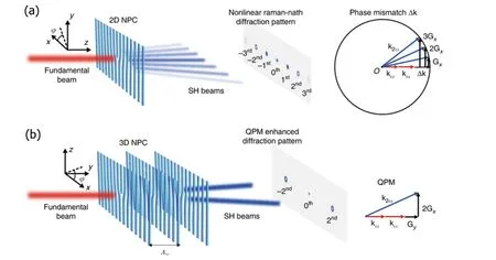
FIG.15.Design principle of 3D NPCs.(a)SH diffraction pattern generated when a fundamental beam is incident on a 2D nonlinear fork-grating NPC.(b)3D nonlinear fork-grating array and the enhanced SH beams.(Reprinted from[62]via the Creative Commons Attribution License.©2019,Springer Nature.)
beam shaping[62],as shown in Fig.15.Different 3D nonlinear grating structures were fabricated to produce the target SH vortex and HG beams.The conversion efficiency of SH beam shaping in a 3D LN NPC with a length of tens of micrometers was enhanced by up to two orders of magnitude compared with the case of 2D LN NPCs.The conversion efficiency can be further improved by increasing the length of the 3D LN NPC.It should be noted that 3D barium calcium titanate(BCT)NPC was also realized by fs-laser poling method[86,87].Through the fs-laser engineering of 3D χ(2)modulations in LN crystals,more complex nonlinear photonic structures for the accurate 3D manipulation of nonlinear optical waves can be fabricated.Therefore,this fs-laser technology paves a way for efficient nonlinear beam shaping[88],nonlinear imaging[89,90],and 3D nonlinear holography[13]for applications in optical communication,super-resolution imaging,and high-dimensional entangled sources.
In 2020,Imbrock et al.[91]reported the first integration of a 3D light-induced quasi-phase-matching structure in the core of an LN waveguide for efficient advanced QPM.The waveguide included a multiscan χ(2)QPM grating and 2D circular type-II waveguide,as shown in Fig.16.To extend the structure to 3D,they split the gratings(blue parts in Fig.16)into two and four parts,respectively.The split waveguide core was able to realize parallel multi-wavelength frequency conversion.They also proposed the concept of a helically twisted nonlinear photonic structure for SH vortex generation and showed the potential for nonlinear beam-shaping devices.The integration of 3D QPM structures into waveguides increased the conversion efficiency,which opens a new avenue to develop ultracompact devices for advanced QPM.

FIG.16. Illustration of a light-induced quasi-phasematching(LiQPM)waveguide that consists of a multiscan grating and circular type-II waveguide fabricated in a single inscription sequence.(Reprinted with permission from[91].©The Optical Society.)
V.CONCLUSION
In summary,we presented a brief review of the fs-laser micromachining of LN crystal. Compared with other micromachining methods,fs-laser technology opens a new way to fabricate complex 3D structures,which widens the application prospects of LN crystals.Fs-laser micromachining has allowed the experimental demonstration of many cutting-edge photonic devices,such as micro-disks and 3D NPCs.Future research will continue to focus on applications of linear and nonlinear photonic devices.Increasingly complex photonic structures could be fabricated using fs-laser micromachining.Fs-laser micromachining of LN crystal is an active topic and related research is ongoing.
ACKNOWLEDGMENTS
This work was supported by the National Key R&D Program of China(2017YFA0303703 and 2016YFA0302500),the National Natural Science Foundation of China(NSFC)(91950206 and 11874213),and Fundamental Research Funds for the Central Universities(021314380105).

