Vapor-Liquid-Solid Growth of Bi2O2Se Nanoribbons for High-Performance Transistors
Congwei Tan, Mengshi Yu, Shipu Xu, Jinxiong Wu, Shulin Chen, Yan Zhao,2, Cong Liu,Yichi Zhang, Teng Tu, Tianran Li, Peng Gao, Hailin Peng,2,*
1 Center for Nanochemistry, Beijing Science and Engineering Centre for Nanocarbons, Beijing National Laboratory for Molecular Sciences, College of Chemistry and Molecular Engineering, Peking University, Beijing 100871, P.R.China.
2 Academy for Advanced Interdisciplinary Studies, Peking University, Beijing 100871, P.R.China.
3 Electron Microscopy Laboratory, International Center for Quantum Materials, School of Physics, Peking University,Beijing 100871, P.R.China.
Abstract:Nanostructured bismuth oxyselenide (Bi2O2Se)semiconductor, a two-dimensional (2D) materials with highmobility, air-stability, and tunable bandgap, has recently emerged as a candidate of channel material for future digital (electronic and optoelectronic) applications.In terms of material morphology, some basic issues will be addressed when a twodimensional layered crystal is shaped into a one-dimensional(1D) geometry due to size effect; these include the spaceconfined transport in a plane, which leads to dramatic changes in electronic, optical, and thermal properties.These novel 1D nanostructures with unique properties are an optimal choice for fabricating next-generation integrated circuits and functional devices within the nanometer scale such as gate-all-around field-effect transistors, single-electron transistors,chemical sensors, and THz detectors.As one of the high-mobility 2D semiconductor, 1D high-quality Bi2O2Se nanoribbons could be promising for applications in high-performance transistors; however, their synthesis has not been completely developed yet.In our study, we report on the facile growth of Bi2O2Se nanoribbons on mica substrates via a bismuthcatalyzed vapor-liquid-solid (VLS) mechanism.The preparation of Bi2O2Se nanoribbons is based on a previous work that emphasized on the oxidation of Bi2Se3 in a chemical vapor deposition (CVD) system and the use of bismuth (Bi) particles as the precursor of Bi catalysis.The morphology, composition, and structure of the as-grown Bi2O2Se nanoribbons were characterized by scanning electron microscopy (SEM), atomic force microscopy (AFM), Raman spectroscopy, transmission electron microscopy (TEM), as well as other methods.For a Bi mediated VLS growth process, the growth of Bi2O2Se nanoribbons can be self-assembled; further, in this process, as-grown epitaxial Bi2O2Se nanoribbons are free-standing with out-of-plane morphology on the mica substrate.Additionally, combining the spherical aberration corrected transmission electron microscope (ACTEM) and selected electron diffraction (SAED) methods, we discovered that the assynthesized Bi2O2Se nanoribbons were single crystalline with high quality.We further investigated the controllable growth for domain size by optimizing the growth temperature of the Bi2O2Se nanoribbons.As-synthesized single-crystal Bi2O2Se nanoribbons have widths in the range of 100 nm to 20 μm and lengths in the sub-millimeter range.By employing a polymer poly(methyl methacrylate) (PMMA) assisted clean transfer method with the assistance of deionized water, the Bi2O2Se nanoribbons can be easily transferred onto a SiO2/Si substrate.Fabricated into the top-gated field-effect device, the Bi2O2Se nanoribbon sample (transferred to the SiO2/Si substrate) exhibited high electronic performances; these included a high electron mobility of ~220 cm2·V-1·s-1 at room temperature, good switching behavior with on/off ratio of >106, and high on current density of ~42 μA·μm-1 at a channel length of 10 μm.Therefore, Bi2O2Se nanoribbons are expected to be a promising materials for building high-performance transistors in the future.
Key Words:Bismuth oxyselenide;Vapor-liquid-solid growth;Nanoribbons;CVD;High mobility
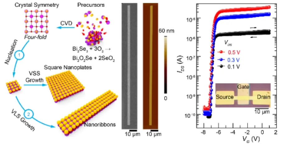
1 Introduction
Fabricating advanced technological-node transistors and manipulating electronic properties of two-dimensional (2D)materials hold significance for their future applications in nanoelectronics, for which converting a two-dimensional to onedimensional (1D) structure (nanowires, nanotubes, and nanoribbons) is an effective strategy.For future technology nodes, gate-all-around field effect transistors (FETs) fabricated on a 1D semiconductor nanostructure are promising candidates to replace the fin-field effect transistors (FinFETs) Fin Field Effect Transistors and planner short-channel FETs owing to a better electrostatic control of the channel transport and facilitating further reductions in transistor size with low leakage currentsviafully surrounding gate1,2.As the technology node requires to control channel diameter in the sub-3 nm range,except for 2D semiconductor with 1D geometry, most channel materials (Si, Ge and III-V) face process, mobility or quantum capacitance challenges of such ultra-thin body thickness3,4.Besides, some basic issues will be addressed as 2D layered crystal shape into a 1D geometry, such as space-confined transport in a plane and leads to dramatic changes in electronic,optical, and thermal properties1,2,5.Graphene nanoribbons, as a typical example, varies from pristine 2D graphene nanosheets and exhibits non-zero bandgap useful for room temperature transistor operations with excellent switching speed and high carrier mobility4,6,7.Besides, many other ribbon-like 2D materials, such as MoS28, phosphorene9,10, WSe22, and Bi2Se311nanoribbons, also lead to exceptional control over electronic structure, by which the novel quantum phenomena and unique electric properties can be observed.In this regard, fabrication of 2D materials into 1D nanoribbons (varying from the 2D) is capable of arousing scientific and technological interests.
In terms of 2D materials, a currently arising member, bismuth oxyselenide (Bi2O2Se), joins the family of layered 2D materials and emerges as a promising candidate for future electronic and optoelectronic applications12-15.Bi2O2Se has been demonstrated to be of among remarkable characteristics, such as air stability against oxidation and moisture12, tunable bandgap with the thickness down to a few atomic layers12,16, high electron mobility (> 20000 cm2·V-1·s-1at 1.9 K)12,16-18, being accessible to single crystal films on a wafer-scale19.In addition, Bi2O2Se exhibits high sensitivity, ultrafast broadband photoresponse(0.3-1.7 μm of wavelength)13, and ultrabroadband saturable absorption for the mid-infrared (5.0 μm)20.Interestingly, a strain may even induce the giant polarizations, resulting in piezoelectricity and ferroelectricity of Bi2O2Se21.These attractive properties make 2D Bi2O2Se became a candidate for creating future infrared photodetector and high-performance electronic devices.Therefore, similar with other 2D materials, it is highly motivated that synthesizing 1D Bi2O2Se nanoribbons for realizing potential applications of Bi2O2Se among highperformance transistors, but the reliable preparation of Bi2O2Se nanoribbons with chemical method remains challenging.
Here,viafacial bismuth (Bi)-catalyzed vapor-liquid-solid(VLS) growth mechanism, we present a chemical vapor deposition (CVD) method to synthesize high-quality Bi2O2Se nanoribbons.In this mean, Bi is used as catalyst to induce the orientated growth of the Bi2O2Se, especially at out-of-plane,resulting in formation of one-dimensional nanoribbons.The bottom-up synthesized Bi2O2Se nanoribbons have typical width down to ~100 nm, thickness down to 5 nm and length up to 200 μm.A polymer assisted clean transfer method was developed to transfer the Bi2O2Se nanoribbons onto the SiO2/Si substrate.Fabricated into the FET, the Bi2O2Se nanoribbon sample(transferred to the SiO2/Si substrate) exhibited high electronic performances: high electron mobility of ~220 cm2·V-1·s-1and large current on/off ratios of > 106.
2 Experimental and computational section
2.1 Synthesis of Bi2O2Se nanoribbons
The preparation of Bi2O2Se crystal is based on previous work on the oxidation of Bi2Se3 in CVD system16.Here, we further extend this methodology to prepare Bi2O2Se nanoribbonsviaBicatalyzed VLS growth.The Bi2O2Se nanoribbons were synthesized by the home-made double-zone CVD system(Thermo Inc.), which equipped with a 12-inch-long and 30-mmdiameter quartz tube.Typically, Bi particles (Alfa Aesar,99.999%) were place in the upstream zone, and Bi2Se3bulks(Alfa Aesar, 99.999%) were place in the second zone.The freshly cleaved mica substrates were place on top of Bi2Se3bulks with a gap of ~3-5 mm.The mixed carrier gas was high-purity Ar/O2gas with typical flow rate of 100 sccm/30 ppm (sccm:standard-state cubic centimetre per minute, 1 ppm = 1 × 10⁻⁶(volume fraction)), and the pressure of the system was kept at 400 Torr (1 Torr = 133 Pa).The growth range was about 590-620 °C.
2.2 Characterization of Bi2O2Se nanoribbons
The morphology of the Bi2O2Se nanoribbons was characterized by OM (Olympus DX51 microscope), AFM(Bruker icon), and SEM (Hitachi S4800 field emission).The structure and crystallinity of as-grown Bi2O2Se nanoribbons was performed using transmission electron microscopy (TEM, FEI Tecnai F30 and FET Titan Themis G2 operating at 300 kV) with energy-dispersive X-ray (EDX) mapping capabilities.Samples for TEM characterization were transferred onto the carbon film supported gold grids by a polymethyl methacrylate (PMMA)-mediated transfer method with the assistance of deionized water22.Raman spectra and mapping was performed at a wavelength of 633 nm on Scanning near-field Raman spectrometer (Witec RSA300+ optical microscope).
2.3 Fabrication of Bi2O2Se-nanoribbon-based FET device
To build top-gate FETs, the Bi2O2Se nanoribbons were transferred onto 300 nm SiO2/Si substrates with the location markers using PMMA-mediated transfer method under the assistance of deionized water.The electron beam lithography(EBL, FEI Inc.) was adopted to pattern the electrodes (source,drain, and top-gate electrode) in two steps.Firstly, the source and drain electrodes were patterned with standard EBL process,followed with the metal deposition (Pd/Au, 5 nm/40 nm) by thermal evaporation.Secondly, the top-gated electrodes required a second EBL exposure to exploit the ‘window’ for the deposition of the high-κ top-gate dielectric HfO2(20 nm) by atomic layer deposition (ALD), then 5 nm/40 nm Pd/Au films were deposited as the top-gate electrode.The as-fabricated Bi2O2Se-nanoribbon-based top-gate FETs were measured under ambient conditions on a semiconductor analyzer (Keithley, SCS-4200) combined with micromanipulator 6200 probe station at room temperature.
3 Results and discussion
Upon the Vapor-solid-solid (VSS) growth mode, various synthesis process for Bi2O2Se generally tends to form 2D structure (square nanoplates) with a characteristic crystal shape12,16,22-25(Fig.1a).In VSS process, determined by the inherent free energy of crystal edges and surface diffusion kinetics, the gas/vapor phase precursors are converted to solidstate products to form the in-plane 2D nucleiviasurface adsorption on the substrate, resulting in the formation of the native 2D layer structure8,26.To prepare 1D morphology, VLS growth is effective mechanism to guide the directed growth of nanostructure, in which 1D nanostructures are synthesized by precipitation from supersaturated catalytic liquid droplets.To this end, we conducted Bi-catalyzed CVD approach to realize VLS growth mode to synthesize the 1D Bi2O2Se nanoribbons using Bi2Se3 and O2 as precursors (see Experimental for details).Particularly, there are two advantages for using Bi as a catalyst:(1) Bi acts as a catalyst to realize the VLS growth mechanism for preparation of Bi2O2Se nanoribbons27-30; and (2) Bi still acts as a reaction precursor to achieve rapid growth of Bi2O2Se nanoribbons according to the thermodynamic phase diagram of Bi2O2Se16.
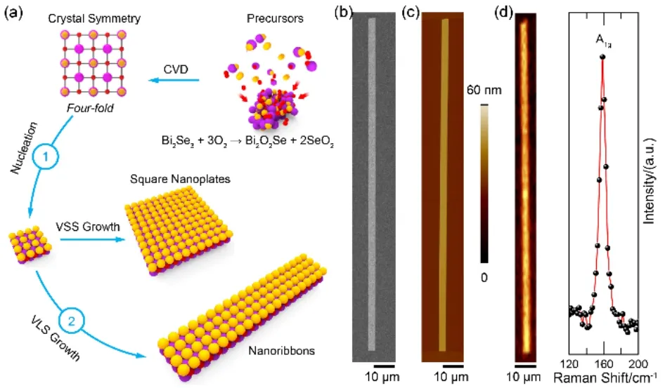
Fig.1 One-step bottom-up synthesis of Bi2O2Se nanoribbons.
As shown in Fig.1b, the as-grown crystal shows a ribbon-like morphology with the length of sub-millimetre.The atomic force microscopy (AFM) characterization reveals that the surface of the as-grown sample is clean and homogeneous, and its thickness is around 10 nm with a width of 2 μm.Furthermore,Raman spectroscopy indicates that the characteristicA1gpeak of Bi2O2Se located at ~159 cm-1, which is good consistent with the prior reports15, confirming that as-synthesized nanostructures are Bi2O2Se nanoribbons.In addition, the Raman mapping of A1gpeak is very uniform across the whole nanoribbon,demonstrating the high uniformity of as-synthesized Bi2O2Se nanoribbons.
To study the phase purity and crystalline nature of as-grown Bi2O2Se nanoribbons, we performed characterization of transition electron microscopy (TEM).The as-synthesized Bi2O2Se nanoribbons were transferred onto the holey carbonsupported Au grid for TEM characterizationviaa polymethyl methacrylate (PMMA)-mediated method.Low-magnitude TEM image shows that the Bi2O2Se nanoribbon has a uniform width along the entire length with typical widths of 500 nm (Fig.2a).As shown in Fig.2b, the selected-area electron diffraction(SAED) pattern reveals single set of diffraction peaks with the four-fold symmetry, verifying that it is a single crystal in asgrown Bi2O2Se nanoribbon.High-resolution TEM image of the Bi2O2Se nanoribbon with a schematic of the atomic positions shows well defined lattice spacing of 0.38 nm, which correspond to the theoretical value of lattice for (100) planes in Bi2O2Se15.Besides, no obvious defects, such as vacancies, interstitials, and dislocations are observed, suggesting that as-grown Bi2O2Se nanoribbons have high crystallinity and purity.As characterized by energy-dispersive X-ray spectrometry (EDS), the obvious signal peaks for Bi, O, and Se were observed (Fig.2d) without other signal of impurities, the element ratio of Bi, O, Se was about 2 : 2 : 1, which is in accordance with the stoichiometry of Bi2O2Se.In addition, corresponding elemental mapping analyses(Fig.2e) further indicates the uniformity without any impurities,suggesting that the Bi2O2Se nanoribbons has good stoichiometry and high purity.
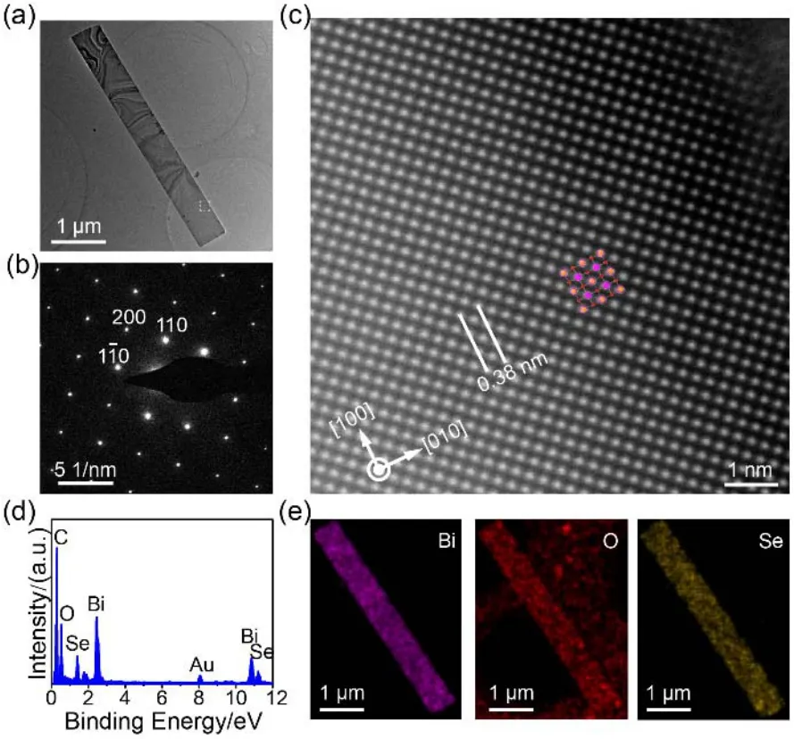
Fig.2 Structural and crystalline quality characterization of Bi2O2Se nanoribbons.
Similarly, some reports have been demonstrated on the catalysis approach for the VLS growth of nanoribbons and nanowire using Bi as catalyst27-30.As shown in the scanning electron microscopy (SEM) images (Fig.3a), as-synthesized Bi2O2Se nanoribbons is out-of-plane on the mica substrate,indicating a Bi mediated VLS growth process.Notably, together with TEM analysis, almost no Bi droplets are found at the tip of Bi2O2Se nanoribbons, this is owing to the complete evaporation of Bi of the surface during the cooling process27,28.Interestingly,although the external perturbation is slight, long and thin out-ofplane Bi2O2Se nanoribbons can be easily broke from their root.As indicated in Fig.3b, c, the as-synthesized thin Bi2O2Se nanoribbons quickly broken from their root under the lowvoltage SEM irradiation (the voltage is 1 kV).Accordingly, it can be inferred that the nanoribbons on the substrate surface are formed by the fracture of thin out-of-plane Bi2O2Se nanoribbons due to the perturbation of cooling process (Fig.1b and 3d).
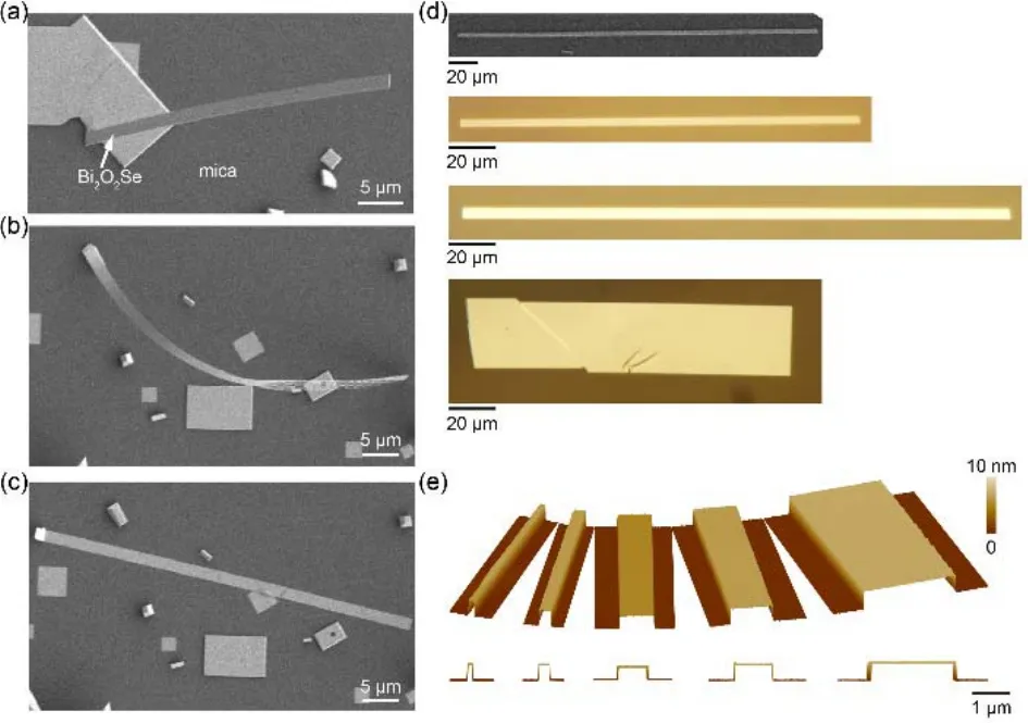
Fig.3 VLS growth of Bi2O2Se nanoribbons on mica substrate.
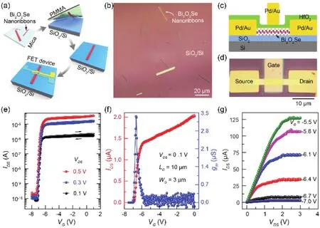
Fig.4 Fabrication and characterization of FET transistor based on Bi2O2Se nanoribbons.
The ability to tailor the diameter of Bi2O2Se nanoribbons for specific applications is essential for synthetic chemistry.In synthesis of Bi2O2Se nanoribbons, varying growth temperature allows considerable control over the diameter of the products.As show in Fig.3d, the length of as-grown Bi2O2Se nanoribbons reached a large value of ~280 μm as temperature varied from 590 °C to 610 °C, and it shrank gradually as further increasing the growth temperature.The approximate reason for the above phenomenon can be summarized as follows.There are two other factors that affect the Bi-catalyzed VLS growth: the low vapor pressure of Bi and the rapid reaction of Bi in the presence of oxygen and selenide (the reaction is 4Bi (l) + Se2(g) + 2O2(g) →2Bi2O2Se (s/l)).When the growth temperature was relatively low, the absorption rate of the Bi-catalyst on the tip of Bi2O2Se nanoribbons is relatively high, the catalyzed effect is dominated in VLS process, leading to growth of long and thin nanoribbons.As elevate to high temperature, the evaporation and chemical reaction of Bi is superior to catalyzed effect, the absorption rate of Bi-catalyst diminishes and the catalyzed effect gradually becomes the dominating elemental step for the growth, resulting in wider and shorter of Bi2O2Se nanoribbons.Notably, naturally folded without breaking in Bi2O2Se nanoribbons can occasionally be formed (Fig.3d), suggesting that ultrathin nanoribbons are rather flexible.Therefore, upon the aforementioned analysis, as shown in Fig.3e, we can reliably obtain the thin nanoribbons with different widths and thickness of 5 nm by controlling the growth time under the low temperature (590 °C).
Generally, the direct transfer of Bi2O2Se nanoribbons on SiO2/Si substrates would enable their wide-ranging applications in photonics or electronics because almost all integrated circuits are rooted in the silicon substrate.Hence, as-grown Bi2O2Se nanoribbons were firstly transfer onto 300 nm SiO2/Si substrates to fabricate the FET devices (Fig.4a).As illustrated in Fig.4b,as-synthesized Bi2O2Se nanoribbons can be easily transfer on SiO2/Si substrates with various width from Mica substrates,which allow us to evaluate their electronic properties conveniently.
To identify the electronic properties of the nanoribbons, a topgated device configuration was adopted to evaluate the switching behavior of Bi2O2Se nanoribbons with a thickness of 15 nm (Fig.S1, Supporting Information).The structure diagram of Bi2O2Se-nanoribbons-based FET devices, and corresponding optical image showing an as-fabricated FET device with a gate length (LG) of 10 μm and width (W) of 3 μm is shown in Fig.4c,d, respectively.As shown in Fig.4e, the measured roomtemperature transfer characteristics verify a n-type transistor behavior with a high current on/off ratio (Ion/Ioff) of ~106at low bias (the level ofIon/Ioffis > 104for practical logic transistors)and small subthreshold slope (SS) of ~75 mV·dec-1.Based on the equationwhereLis the channel length (here,Lequal toLG),Wis the channel width,CGis the capacitance between the channel and the top-gate per unit area(CG=ε0εr/d,ε0 is vacuum permittivity,εr is the relative permittivity, anddis the thickness of HfO2 layer), the field-effect mobility of Bi2O2Se-nanoribbons-based FET devices could be calculated by fitting the linear region in transfer curve (Fig.4f).The field-effect mobility was extracted as ~220 cm2·V-1·s-1, which is the same order as the reported value in a Hall mobility11,18.Besides, the output curves plotted in Fig.4g shows that the high current density (IDS/W) of ~42 μA·μm-1can be achieved.These electronic properties, together with its easy transfer, make Bi2O2Se nanoribbons a promising semiconductor candidate for future low-power logic transistors.
4 Conclusions
In conclusion, we have demonstrated the VLS growth of Bi2O2Se nanoribbons on Mica substrateviaBi-catalyzed CVD.The VLS growth mode is probably conducted by the formation of a Bi liquid solution on the tip of Bi2O2Se nanoribbons.The width and length of Bi2O2Se nanoribbons were controlled by tuning the growth condition (growth temperature and time).In particular, the as-grown Bi2O2Se nanoribbons can be easily transfer onto arbitrary substrates (such as SiO2/Si).The high electrical performance (high mobility, high current on/off ratio,and high on current density) of Bi2O2Se-nanoribbon-based transistors suggest that Bi2O2Se nanoribbons is a promising materials for fundamental investigations and high-performance electronic applications such as Gate-all-around FETs31,32and trigate FETs33.
Supporting Information:available free of chargeviathe internet at http://www.whxb.pku.edu.cn.

