
Modeling of Canonical Switching Cell Converter Using Genetic Algorithm
2017-03-13 05:00:01VikneshandManikandan
T. V. Viknesh and V. Manikandan
1 Introduction
In all the domestic, commercial and military applications, power electronic converters are essential elements in utilization part of power network. Due to the higher efficiency, light weight, and low cost, the switching DC-DC converters have generated a significant research in area of modeling, analysis and control. The building blocks of the converters are inductors, capacitors, resistor and switching elements [VashistBist, BhimSingh,(2014); Divya NavamaniJayachandran, VijayakumarKrishnaswamy,LavanyaAnbazhagan and KarthikeyanDhandapani (2015);C.T. Rim,G.B. Joung,G.H.Cho, (1988)]. These converters must be examined and investigated in terms of their component relationships and topographical characteristics to design and develop well suited converter for our required applications. The canonical converters are playing vital role in DC-DC (boost-buck) conversion in solar panel charge controllers.
1.1 State space model
Many dynamic systems of engineering, biological, social and economic systems can be easily modeled and completely characterized using state space modeling technique. To analyze any system, it is essential to reduce the complexity of the mathematical expressions, as well as to resort to computers for most of the tedious computations necessary in the analysis; state-space approach is best suited for this purpose. Many state space models are used widely to study static and dynamic characteristics of converter as well as to design their control system to achieve specific regulation characteristics[Mohammad Reza Modabbernia, Ali Reza Sahab, Mohammad TaghyMirzaee,KazemGhorbany. (2012)]. State space concepts provide the access to what is going inside the system in addition to input and output mapping. State space modeling is a mathematical model of a physical system as set of input, output and set of variables related by first order differential equation. State space refers to Euclidean space in which variables on axes are state variables. The state of the system can be represented as vector within space. In the system (circuit), the number of state variables is equal to number of independent energy storage elements in it. The dynamic systems are linear, time variant and finite dimensional, then the differential and algebraic equation are written in matrix form. The time domain representation provides convenient and compact way to model and analyze the systems with multiple input and outputs [PretiTyagi, V. C. Kotak, B.Mathew, V. P. Sunder Singh. (2014); J. C. Mayo-Maldonado, R. Salas-Cabrera, H.Cisneros-Villegas, M. Gomez-Garcia, E. N. SalasCabrera, R. Castillo-Gutierrez and O.Ruiz-Martinez. (2010); J.C.Mayo- Maldonado, R. Salas-Cabrera, J.C. Rosas-Cario, J. De Leon- Morales, and E. N. Salas- Cabrera. (2011)].
1.2 Canonical switching cell (CSC) converter
CSC converter is a buck-boost DC-DC converter and it has less number of devices, such as inductor, resistor, capacitor, diode and switch as shown in fig.1. It works mainly in two different modes as i) switch on mode and ii) switch off mode. There is energy transfer between L and C2. The circuit’s characteristic parameters are useful in constructing such CSC converters for DC-DC conversions.
2 State space modeling of CSC
2.1 Five stages of work
1)The various components and their parameters in the circuit were identified and classified as constant parameters, input, state variable and output parameters of CSC.
2)The state space equations of the CSC during ON and OFF states were obtained by using Kirchhoff’s laws. Then the state space matrices for both ON and OFF states were written.
3)The step response graphs were simulated using the matrices in Matlab for both ON and OFF states.
4)The ON and OFF states transfer functions were obtained by using Matlab.
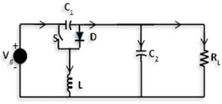
Figure 1: Canonical switching cell converter
5)Using Simulink, a closed loop block was designed and simulated by using the obtained kp, kiand kdvalues till to obtain the perfect response curves the parameters like rise time,settling time, overshoot, and stability were analyzed. In order to obtain the steady state within very short time, the PID tuning technique was introduced using the genetic algorithm.
2.2 CSC converter components and modeling parameters
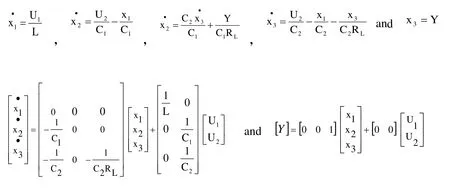
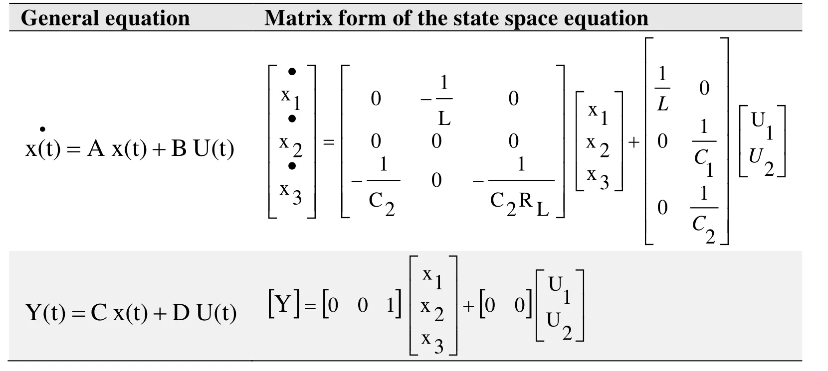
This circuit contains three energy storing devices i) inductor (L), ii) capacitor (C1) and iii)capacitor (C2). The physical quantities of the converter are represented in state space notation as below.
The input, state variable and output quantities were assumed
Input parameters: Vg(U1), and i (U2)
State variables : iL(x1), VC1(x2), and VC2(x3)
Output parameter: V0(Y)
The other parameters such as L, C1, C2and RLare considered as constants and to be optimized for the best performance.
2.3 State space model for CSC converter in ON state
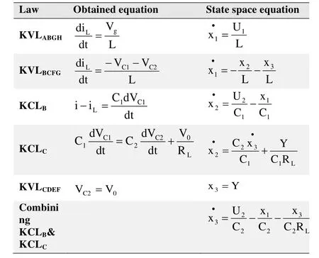
During the ON state of the switch (S), the equivalent circuit of the converter is as shown in fig.2. The mathematical formulations of the circuit are stated with basic laws.Kirchhoff’s current law and Kirchhoff’s voltage law are used at the junctions and in the loops of the converter and the corresponding state space equations are obtained as below.

Figure 2: Canonical switching cell converter in ON state
Using the Kirchhoff laws in the loop ABGH, and at the junctions B, and C, the following state space equations are obtained (Annexure I)
2.4 State space model for CSC converter in OFF state
During the OFF state of the switch (S), the equivalent circuit of the converter is as shown in fig.3. Similar to ON state, mathematical formulations of the circuit are stated with basic laws. Kirchhoff’s current law and Kirchhoff’s voltage law are used at the junctions and in the loops ABGH and CDEF and at the junction B of the converter and the corresponding state space equations are obtained as below. (Annexure II)

Figure 3: Canonical switching cell converter in OFF state

3 Simulation details
The above obtained state space model of the CSC was simulated using MATLAB. The simulation work was executed using the software MATLAB 2016a in a Pentium 4 core i6 computer. The step response graphs were simulated for both ON and OFF states. Then the ON and OFF states transfer functions were obtained then PID controller with Genetic Algorithm tool, the response curves were simulated and the obtained kp, ki and kd values were noted. Using Simulink, a blank model was taken and a closed loop block was designed and simulated using the obtained kp, ki and kd values till to obtain the perfect response curves.
The value of the circuit elements and other input and output parameters of the converter are evaluated from the following ways. The input and output voltages, switching frequency, and efficiency are taken as 12 V, 12 V, 200 KHz and 99 % respectively. The constants such as the value of load resistor(RL), inductor (L)and capacitors (C1and C2) are assumed in the range of 0.1 to 100 Ω,5 x 10-3to 50 x 10-3H, 10 μF and 1to 100μF
4 Simulation results
4.1 Step response analysis
The performance of the CSC was studied using the step response curve simulated using Matlab for both ON and OFF states using state space matrices using the below mentioned MATLAB code. The various values of L, C1, C2and RLwere included in the space matrices and their step response were studied using the step response graph. The optimized values of Load resistance (RL) Inductor (L) Capacitors (C1andC2) are≤1Ω,5mH, 10 μFand10 μF respectively.
MATLAB simulation work was executed using the software MATLAB 2016a with a Pentium 4 i6 computer, the step response graphs were obtained for both ON and OFF states as shown in figure 5. The graphs are exactly like each other and their values are lying within few nano seconds, the graphs show that they are highly stable in nature. The characteristic parameters such as rise time, overshoot, settling time, steady state error and stability aredetermined. The rise time and settling time are 4 x 10⁻⁸s and 8 x 10⁻⁸s respectively but the amplitude is 0.1 instead 1. The optimization tasks were analyzed and then PID tuning technique with genetic algorithm was chosen and incorporated as follows.
The response curve shows no overshoot and very high stable in nature.
4.2 CSC converter fed with PID controller
4.2.1 Simulation results for CSC converter in ON state
The simulated transfer function for this state

The obtained PID parameters using GA are 894 (kp), 446 (ki), 1088 (kd). The transfer function and PID values were incorporated in the below Simulink block (fig. 6). The step function was fixed with maximum value of 12 and step time as 0.01 and simulated. The obtained graph is free from overshoot. The rise time and settling time are in the order of milli seconds.

Figure 4: Step response of the CSC converter during ON and OFF states

Figure 5: Closed loop CSC converter in ON state using Genetic algorithm based PID controller
4.2.2 Simulation results for CSC converter in OFF state
The simulated transfer function for this state

The obtained PID parameters using GA are 266 (kp), 1370 (ki), 2000 (kd). The transfer function and PID values were incorporated in the below Simulink block (fig. 8). The step function was fixed with maximum value of 12 and step size as 0.01 and simulated. The obtained graph is free from overshoot. The rise time and settling time are in the order of milli seconds.
5 Conclusion
The function of the CSC converter was identified and the circuit in ON and OFF states were recognized for modeling. The inputs (Vg, and i), state variable (iL, VC1, and VC2) and output (V0) were assigned to do state space model. State space model of CSC converter in ON and OFF states were developed using the Kirchhoff’s laws. The state space matrices were derived to construct the transfer functions of ON & OFF states. The step response of the converter was simulated using MATLAB. The response curve corresponding to the circuit element values as shown in table 8, shows no overshoot and very high stable in nature. The step response curve was obtained and analyzed using different values of circuit elements and the optimized data was identified as rise time and settling time are 4 x 10⁻⁸s and 8 x 10⁻⁸s respectively but the amplitude is very meager. The Genetic algorithm used PID controller was used to attain the expected amplitude for both ON and OFF states. The obtained PID parameters (894 (kp), 446 (ki), 1088 (kd) for ON state, and 266 (kp), 1370 (ki), 2000 (kd). for OFF state) were entered in the PID block in simulation of ON and OFF states. The obtained graphs are free from over shoot, rise and settling time in the order of 10 milli seconds, and the maximum amplitude (12) as expected in these cases. The excellent results of circuits characteristic parameters is very useful guideline for constructing such CSC converters for DC-DC conversions especially in maximum power point process in driving solar energy using solar panel.

Figure 6: Closed loop CSC converter in OFF state using Genetic algorithm based PID controller
Acknowledgement The authors would like to express their sincere thanks to Dr. S R K Prasad (Correspondent, CIT), Dr. R.Prabhakar (Secretary, CIT), Dr.V.Selladurai(Principal, CIT), and Mr. S. Rajiv Rangasamy(Director, CIT) for their help and encouragement during the course of work.
VashistBist, BhimSingh, (2014) “A PFC-Based BLDC Motor Drive Using a Canonical Switching Cell Converter” IEEE transactions on industrial informatics, Vol. 10, no. 2.
Divya NavamaniJayachandran, VijayakumarKrishnaswamy, LavanyaAnbazhagan and KarthikeyanDhandapani (2015) “Modelling and Analysis of Voltage Mode Controlled Luo Converter” American Journal of Applied Sciences, 12 (10) page 766-774.
C.T. Rim,G.B. Joung,G.H. Cho, (1988) “A state-space modeling of nonideal DC-DC converters”Power Electronics Specialists Conference at Kyoto in Japan. PESC '88 Record., 19th Annual IEEE ,
Mohammad Reza Modabbernia, Ali Reza Sahab, Mohammad TaghyMirzaee,KazemGhorbany. (2012) “The State Space Average Model of Boost Switching Regulator Including All of the System Uncertainties” Advanced Materials Research,Vols. 403-408, pp 3476-3483
PretiTyagi, V. C. Kotak, B. Mathew, V. P. Sunder Singh. (2014) “State Space Modelling of High Gain DC-DC Boost Converter with Coupling Inductor”International Journal of Engineering Research & Technology (IJERT) Vol. 3 Issue .
J. C. Mayo-Maldonado, R. Salas-Cabrera, H. Cisneros-Villegas, M. Gomez-Garcia,E. N. SalasCabrera, R. Castillo-Gutierrez and O. Ruiz-Martinez. (2010) “Modeling and Control of a DC-DC Multilevel Boost Converter” Proceedings of the World Congress on Engineering and Computer Science 2010 Vol II WCECS 2010, October 20-22, San Francisco, USA
J.C.Mayo- Maldonado, R. Salas-Cabrera, J.C. Rosas-Cario, J. De Leon- Morales,and E. N. Salas- Cabrera. (2011) “ Modelling and control of a DC-DC multilevel boost converter”, IET Power Electron, vol.4, no.6 page 693.
M.Kasperm, D. Bortis and J. W. Kolar. (2014) “Classification and comparative evaluation of PV panel-integrated DC-DC converter concepts”, IEEE trans. Power electron., vol.29, no.5 page 2511-2526.
M. Bella, F. Prieto, S. P. Litran, J. Manuel and E. Gomez. (2016) “New single input multiple output converter topologies” June 2016 page 6-20.
Annexure I
(On state)

Annexure II
(Off state)

 Computer Modeling In Engineering&Sciences2017年1期
- Computer Modeling In Engineering&Sciences的其它文章
- Acoustic Scattering Performance for Sources in Arbitrary Motion
- Inverse Analysis of Origin-Destination matrix for Microscopic Traffic Simulator
- Stability Analysis of Cross-channel Excavation for Existing Anchor Removal Project in Subway Construction
- Optimization of Nonlinear Vibration Characteristics for Seismic Isolation Rubber
- A Study on the Far Wake of Elliptic Cylinders
- Reliability Analysis for Complex Systems based on Dynamic Evidential Network Considering Epistemic Uncertainty