Enhanced photocatalytic degradation of methyl orange by CdS quantum dots sensitized platelike WO3photoelectrodes
WEN Jin(文瑾) ,LIU Can-jun(刘灿军) ,DU Yong(杜勇) ,HU Chuan-yue(胡传跃) ,TIAN Xiu-ying(田修营)
1.Power Metallurgy Research Institute,Central South University,Changsha 410083,China;2.Department of Chemistry and Material Science,Hunan University of Humanities,Science and Technology,Loudi 417600,China;3.School of Chemistry and Chemical Engineering,Central South University,Changsha 410083,China
1 Introduction
As a promising material,tungsten trioxide (WO3)exhibits a band gap of ca.2.6 eV,high photocatalytic activity and nontoxic character [1-2].In recent research,it has been reported that the low-dimensional nanostructured WO3films,such as nanowires [3],nanorods [4-5],and nanoplate [6-7],exhibit superior photocatalytic and PEC properties,compared to those films with nanoparticles.This is mainly because low-dimensional nanostructured films can provide a direct pathway for charge transport and higher charge mobility than nanoparticle films,which can effectively reduce the recombination of photogenerated electrons and holes [8-10].Furthermore,low-dimensional nanostructure usually has the advantage of low reflectance due to light scattering and trapping over a wide spectrum range,resulting in superior optical absorption properties for them [11].
Although WO3is one of the most important materials widely investigated for photodegradation and water splitting,the wide bandgap (Eg≥2.6 eV) of WO3limits its photocatalytic activity in the near UV region[12].To extend the activity of the WO3photoelectrode into the visible light region,various approaches have been taken including doping WO3with other impurities(such as C [13],S [14]and N [15-16]) and coupling with low band-gap semiconductors [17-18]Low band gap semiconductor quantum dots (QDs),such as PbS [19],PbSe [20],CdS [21-22],CdSe [23]and Ag2S [24]that are optically active in the visible light,are of great interest in photovoltaics and photocatalysis because they have many advantages as sensitizers of photoelectrodes.They include the tunable band gap by QDs size [25],multiple exciton generation [26]and extended photostability [27].
Cadmium sulfide (CdS) is a more promising material and has been reported to have better performance for PEC water splitting [28-29]and photoelectrocatalytic degradation of organic pollutants[30-32].Because it has a more suitable band gap (2.4 eV)and a higher conduction band edge than TiO2and ZnO,the photogenerated electrons in the CdS QDs can be transferred to conduction band of TiO2or ZnO under visible light irradiation [33-34].Compared to TiO2or ZnO,WO3has a lower conduction band level (+0.4 eVNHE),so it is reasonable to expect that charge transfers can occur between the CdS QDs and WO3[35-36].But there is little work that has been done on WO3and CdS QDs based composite structures [37-38].This is mainly due to thermodynamical instability of WO3material in alkaline environments and CdS QDs with excellent properties are generally prepared by a CBD technique in an alkaline medium.Thus,in situ loading of WO3photoelectrodes with CdS QDs using suitable and facile methods is still a challenging issue.
In our previous work,we had successfully developed a favorable route for preparing CdS QDs sensitized WO3platelike photoelectrodes with a TiO2buffer-layer.The WO3platelike films were synthetized by hydrothermal RF sputtered tungsten thin films[38].Herein,we report a more facile method to prepare high quality and stability CdS QDs-sensitized WO3platelike photoelectrodes with a TiO2buffer-layer via a combination of hydrothermal and CBD methods.The structural,morphologic and PEC properties of CdS QDs-sensitized WO3photoelectrodes with a TiO2buffer-layer were evaluated.The photocatalytic activity of the photoelectrodes was evaluated by degradation of methyl orange under visible light irradiation.Further,we focus on investigating the effects of the TiO2buffer-layer on photocatalytic and PEC activity.This work would help us to design a new high activity and stability of QDs-based photoelectrodes in the visible light region.
2 Experimental section
2.1 Synthesis and characterization
All chemicals were of analytical grade.WO3platelike films were prepared by hydrothermal method according to the reported literature [39].0.231 g of sodium tungsten dehydrate (Na2WO4·2H2O) as the tungsten source was dissolved in 30 mL of deionized water under constant stirring at room temperature.Then,10 mL of 3 mol/L HCl was added to the solution,followed by the addition of 0.2 g of ammonium oxalate((NH4)2C2O4).After several minutes of stirring,30 mL of deionized water was added into it with continual stirring for 30 min.The as-prepared precursor was transferred into a 100 mL of Teflon-lined stainless autoclave.The FTO substrates with the conducting side facing down were immersed and leaned against the wall of the Teflon-vessel.The hydrothermal synthesis was carried out at 140 °C for 3 h.The as-prepared films were calcined at 450 °C for 1 h.Coating of nano-TiO2on WO3films was achieved by the thermal hydrolysis of TiCl4(Sigma-Aldrich),which have been well documented in Ref.[35].CdS QDs has been deposited onto WO3platelike films by a modified CBD method.To reduce corrosion of the WO3electrodes in the Na2S solution during loading CdS QDs process,anhydrous ethanol and methanol were used as solvent.Firstly,the substrate with WO3platelike films were immersed in 5 mmol/L ethanol solution of Cd(NO3)2for 5 min for the adsorption of Cd2+onto the platelike WO3surface and then thoroughly washed with anhydrous ethanol.Then,it was dipped in 5 mmol/L methanol solution of Na2S for 5 min and thoroughly washed with methanol.The S2-reacted with the absorbed Cd2+forming CdS.This two-step dipping procedure was repeated ten times.
The crystalline phase of the electrodes was characterized by X-ray power diffraction (D/Max2250,Rigaku Corporation,Japan).The surface morphologies of the thin films were investigated by scanning electron microscope (Nova NanoSEM 230).High-resolution transmission electron microscopy (HR-TEM,TECNAI G2 F20,FEI) was operated at 200 kV to observe the crystallinity and arrangement of WO3,TiO2and CdS.The surface electronic states of the films were analyzed using X-ray photoelectron spectroscopy (XPS,K-Alpha 1063,Thermo Fisher scientific).A spectrophotometer(DR-UVS,Shimadzu 2450 spectrophotometer) was used to record the UV-vis spectra in the range 300-800 nm.
2.2 Photocatalytic performance testing
Methyl orange (MO) was considered a model contaminant with an initial concentration of 10 mg/L.The photoelectrocatalytic degradation of methyl orange was carried out in a 60 mL quartz photochemical reactor containing 40 mL of aqueous solution under visible light irradiation at an applied potential of 0.5 V (vs SCE).A 500 W xenon lamp with a cutoff filter (λ>400 nm) was employed as the visible light source.In addition,the fabricated film electrode with an active area of 2.5 cm×2.5 cm,platinum electrode and saturated calomel electrode (SCE) were using as the working electrode,counter electrode and reference electrode,individually.Before irradiation,the film electrode was immersed into the MO solution in a dark room for 1 h to reach the adsorption-desorption equilibrium of MO on the film electrode.The experiments were performed with magnetic stirring at 25 °C and continually bubbled with N2,using 0.1 mol/L NaNO3aqueous solution as supporting electrolyte to enhance the conductivity of the reaction solution [32].At given irradiation time intervals,3 mL of the reaction solution was sampled,and the relative concentration of MO in the solution was analyzed using an UV-vis spectrophotometer (UV2100,Shimadzu) at its characteristic wavelength (λMO=467 nm).
2.3 Electrical and photoelectrochemical measurements
The photoelectrochemical measurement was carried out in a typical three-electrode electrochemical cell.An Ag/AgCl/satd.KCl electrode was employed as the reference electrode and a platinum foil was used as the counter electrode.All the electrodes were performed in a solution containing 0.35 mol/L Na2SO3and 0.25 mol/L Na2S (pH ≈ 11.5) by an electrochemical analyzer(Zennium,Zahner,Germany).A 150 W Xe lamp(CHF-XM35,Beijing Trusttech Co.Ltd.) with a 400 nm cutoff filter to remove UV irradiation was used as the visible light source.The light intensity was adjusted to 100 mW/cm2.
3 Results and discussion
3.1 SEM,XRD,EDS and HR-TEM analyses
The photographs of the WO3film,TiO2/WO3film,CdS QDs/TiO2/WO3film and CdS QDs/WO3film are shown in Fig.1.Compared with the pristine WO3film,the color of the TiO2/WO3film has almost no change,but the color of the as-prepared QDs CdS/TiO2/WO3film and QDs CdS/WO3film obviously changes to yellow.
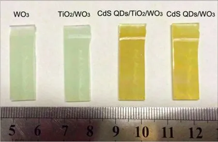
Fig.1 Photographs of film samples
The SEM images observably reveal the high density and uniform vertical alignment of WO3plates grown on a FTO substrate (Fig.2).The pristine WO3plates have a smooth surface and exhibit an edge length in the range of 500 nm-1.5 μm and a thickness of 50-200 nm (Fig.2(a)).As shown in Fig.2(b),the TiCl4-treated WO3plate surface morphology is dramatically different from the pristine WO3.It is evident that a number of small flakes and dots are aggregated to form a thin film on the surface of the plates.After loading CdS QDs,the number of dots obviously increases,which can be clearly seen from Figs.2(c) and (d).
Figure 3 shows the XRD patterns of the WO3film,CdS QDs/TiO2/WO3film and CdS QDs/WO3film.The patterns of the all films correspond to monoclinic WO3(JCPDS No.83-0950),and there are no obvious other peaks,which is likely due to low CdS and TiO2content.The intensity of the diffraction peaks only for CdS QDs/WO3film decreases slightly,compared to the pristine WO3film.This indicates that the crystal structure of the WO3plates probably has suffered slight damage during loading CdS QDs process.The local composition of QDs CdS/TiO2/WO3film was analyzed by an energy dispersive X-ray spectrometer (EDS).

Fig.2 SEM images:(a) WO3film;(b) TiO2/WO3film;(c) CdS QDs/ WO3film;(d) CdS QDs/TiO2/WO3film

Fig.3 XRD patterns of film samples
The EDS analysis over the region of the film shows the existence of Cd,S,and Ti in Fig.4(a).Figure 4(b)shows high magnification TEM image of the as-prepared CdS QDs/TiO2/WO3film.The lattice spacing of WO3is 0.384 nm,which corresponds to the (002) plane of monoclinic WO3(JCPDS No.83-0950),and that of TiO2is 0.354 nm,which match with the (101) plane of anatase TiO2(JCPDS No.71-1167).In addition,the observed lattice spacings of 0.336 nm and 0.206 nm correspond to the (111) plane and (220) plane of CdS (JCPDS No.89-0440).The TEM image also indicates that the size of CdS crystallite rangs between 6 and 8 nm,consistent with the size of dots (< 10 nm).

Fig.4 EDS spectra of CdS QDs/TiO2/WO3film (a) and HR-TEM image of CdS QDs/TiO2/WO3film (b)
3.2.XPS analysis
The composition of the CdS QDs/TiO2/WO3film was further detected by the XPS as shown in Fig.5.Figure 5(a) shows the XPS spectra of W 4f,S 2p,Cd 3d,Ti 2p and O 1s.The peak binding energies are observed at 41.3,37.5 and 35.5 eV,which correspond to spin-orbit splitting of the W 5p3/2,W 4f5/2and W 4f7/2components,respectively,in tungsten oxides (Fig.5(b)).It indicates that the W6+ions are dominant in the sample [40-41].As expected the XPS spectra for Ti display the peaks of Ti 2p3/2and Ti 2p1/2at 459.1 and 37.5 eV clearly assigned to TiO2(Fig.5(c)) [40].In addition,the XPS spectra of the CdS QDs/TiO2/WO3film show the presence of peaks at 405.3 eV and 412.1 eV corresponding to Cd2+and at 161.6 eV and 162.7 eV corresponding to S2-(Figs.5(d)and (f)) [42-43],further conforming the formation of the CdS QDs.On the basis of the above analysis results,it can be concluded that high-quality CdS QDs/TiO2/WO3films have been successfully fabricated using a modified CBD method.
3.3 UV-visible optical absorption
Figure 6 illustrates the UV-visible optical absorption spectra of the WO3,QDs CdS/WO3and QDs CdS/TiO2/WO3films.For the WO3film,the onset position of light absorption is about 460 nm.It is clear that the deposition of QDs CdS on the surface of WO3plates results in better absorption in visible light.Relative to the absorption edge of the pristine WO3film,the spectral positions of the absorption edge red shift to about 536 and 538 nm for the QDs CdS/WO3and QDs CdS/TiO2/WO3films,respectively.The band gap (Eg) of the films could be estimated by the Tauc formula using the following relation:

whereαis the absorption coefficient,hvis the energy of incident photon;Ais a constant;ηis equal to 2 for a direct band gap and 1/2 for an indirect band gap.The transitions of CdS and WO3are direct and indirect,respectively.According to the above formula,the band gaps of the WO3,QDs CdS/WO3and QDs CdS/TiO2/WO3films were estimated to be about 2.70,2.31 and 2.30 eV respectively,which are consistent with the other reports [37,44].The both band gaps of QDs CdS/WO3and QDs CdS/TiO2/WO3films are larger than that of CdS in the bulk (2.25 eV),suggesting that the size of CdS particles on the film is within the scale of QDs.There are the very similar values for the both band gaps of QDs CdS/WO3and QDs CdS/TiO2/WO3films,indicating the similar size of CdS particles in the two films [45].
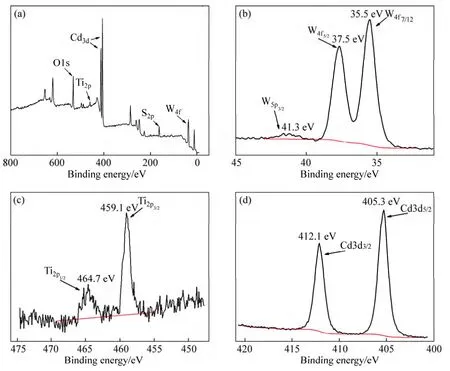
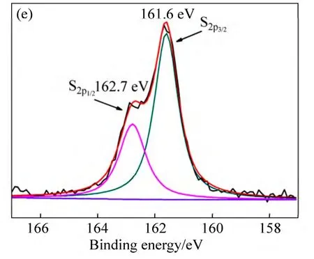
Fig.5 XPS survey of spectrum (a) and spectra of W (b),Ti (c),Cd (d) and S(e)
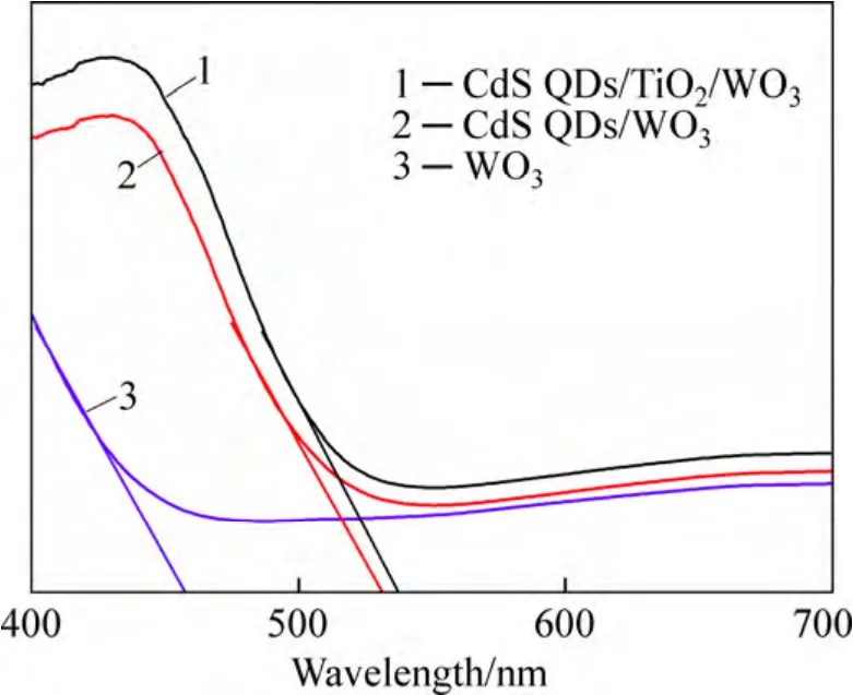
Fig.6 UV-visible optical absorption spectral of film samples
3.4 Photoelectrocatalytic degradation of MO under visible light irradiation
The photoelectrocatalytic (PEc),photocatalytic (PC),and electrochemical (EC) processes of methyl orange(MO) in aqueous solutions were performed on the CdS QDs/TiO2/WO3electrode under visible light illumination(λ>400 nm).The ratio of MO concentrationC/C0could be determined as

whereA0andAare the absorbance values at the wavelength of 467 nm at time 0 andt,respectively;C0andCare the concentrations of MO at irradiation time 0 andt,respectively.The results show that 72.3% of MO was decomposed after 3 h in the PEc process,while only 13.6% and 1.1% of MO were decomposed in PC and EC process during the same illumination time (Fig.7(a)).In the PEc process,an additional bias voltage between the sample electrode and Pt electrode was applied to photoelectrons to migrate to the Pt electrode through the outer circuit,therefore suppressing the combination of electrons and holes and enhancing the efficiency of the photocatalytic reaction.The photocatalytic degradation of MO obeys the first-order reaction kinetics and the kinetic constantkcan be calculated as following relation:

Figure 7(b) demonstrates the kinetic behaviors of MO PEc degradation on the sample electrodes under visible light irradiation.Evidently,the rate constants of the CdS QDs/TiO2/WO3electrodes are higher than those of CdS QDs/WO3and pure WO3electrodes.Not surprisingly,thekof CdS QDs/WO3electrodes started to decrease after 2 h illumination.This is probably because when the concentration of MO reduces to a certain degree,CdS QDs/WO3and CdS QDs/TiO2/WO3electrodes easy suffer from photocorrosion,which leads to catalyst (CdS) damage [46].In a word,this result shows that visible-light-induced catalytic efficiency of the platelike WO3photoelectrodes was improved by the sensitization of CdS QDs.Moreover,CdS QDs/TiO2/WO3electrodes reveal higher photocatalytic activity than CdS QDs/WO3electrodes for degradation of MO.It is probably because the introduction of CdS QDs enhances visible light response and the charge separating junction between TiO2nanoparticles and WO3films can effectively suppress the electron-hole recombination.
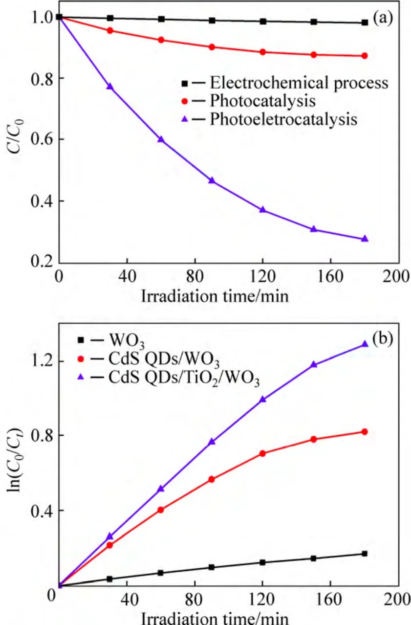
Fig.7 Degrading MO by photoelectrocatalysis,photocatalysis,and electrochemical processes for CdS QDs/TiO2/WO3photoelectrodes (a) and degradation rates of MO of sample photoelectrodes under visible light illumination (b)
3.5 Photoelectrochemical study

Fig.8 Photocurrent density (a) and electrochemical impedance spectra (b) of photoelectrodes
The WO3,CdS QDs/WO3and CdS QDs/TiO2/WO3films were used as photoelectrodes in the PEC cell.The PEC properties of all the electrodes were recorded by linear sweep voltammetry in a potential rang from -1.1 V to 0.1 V (vsAg/AgCl) under darkness and illumination.A 100 mW/cm2Xe lamp was used as the visible light source in 0.35 mol/L Na2SO3and 0.25 mol/L Na2S electrolytic solutions.The linear sweep curves are shown in Fig.8(a).The QDs CdS sensitized WO3electrodes exhibit much higher photocurrent than the pristine WO3electrodes under illumination,which is attributed to the enhanced visible light response.Particularly,the photocurrent density at 0 V (vs Ag/AgCl) of the CdS QDs/TiO2/WO3electrode is 1.65 mA cm-2,which is almost 6 times higher than that of the WO3electrode(0.28 mA/cm2).The CdS QDs/TiO2/WO3electrodes show a little larger photocurrent than CdS QDs/WO3.This likely is because the introduction of nano-TiO2layer on WO3film can improve the electron-injection and transporting property.The photocatalytic activity testing results could also support the hypothesis.To better understand the enhanced PEC property in the CdS QDs/TiO2/WO3photoelectrodes,we also carried out the electrochemical impedance spectroscopy (EIS).Figure 8(b) shows the impedance spectra of WO3,CdS QDs/WO3and CdS QDs/TiO2/WO3photoelectrodes at the applied potential of 0 V (vs Ag/AgCl) in 0.35 mol/L Na2SO3and 0.25 mol/L Na2S under visible light illumination.The smaller semicircle of the EIS Nyquist plot means the smaller charge-transfer resistance in the electrode.The efficient charge transfer reduces the charge recombination,resulting in the facile charge transport of electrons through the electrode and a higher photocurrent.The result is well consistent with the photocurrents measured before,indicating that the CdS QDs/TiO2/WO3photoelectrodes have the superior charge transfer efficiency.
In order to investigate the stability of the photoelectrodes,photocurrent as a function of time of the photoelectrodes was measured at -0.1 V (vs Ag/AgCl)under discontinuous illumination.The results are shown in Fig.9.The photocurrent for all photoelectrodes declines dramatically with time in the first 100 s.The CdS QDs/WO3electrode shows a decrease photocurrent while the photocurrent of the CdS QDs/ TiO2/WO3electrode has almost no decrease in the following 1700 s,indicating that the CdS QDs/TiO2/WO3electrode exhibits good stability in the PEC system.
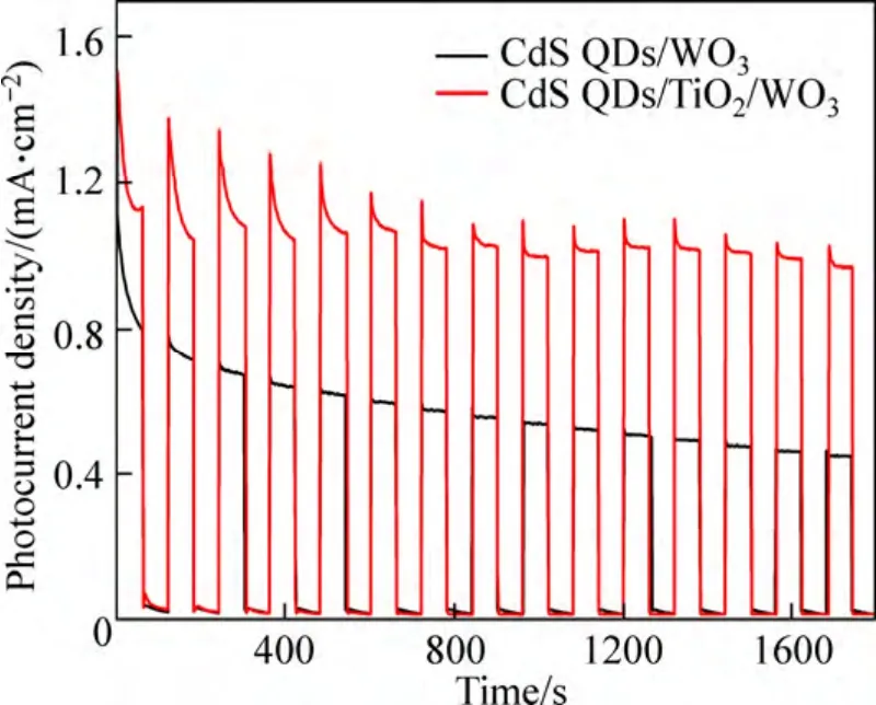
Fig.9 Photocurrent-time plot of photoelectrodes
3.6 Mechanism discussion.
In order to address our process in detail,we designed the architecture and energy band diagram for the photoelectrodes that could explain the possible mechanism for the enhanced photocatalytic and PEC performance under visible light irradiation (Fig.10).From this energy band diagram,it can be seen that the conduction band (CB) level of CdS (-0.4 VNHE) is more negative than the CB of TiO2(-0.1 VNHE),and the CB of TiO2is higher than the CB of WO3(+0.4 VNHE) [36].When the electron-hole pairs are photogenerated in the CdS QDs under visible light illumination,the photoexcited electrons can favorably transfer from the CB of CdS QDs to the CB of TiO2and then to the CB of WO3along the potential gradient.Simultaneously,the holes left in the CdS QDs will be consumed for an oxidation reaction at the electrode/electrolyte interface.Likewise,the photoexcited electrons can also directly transfer to the CB of WO3.Therefore,the junction heterostructure between the CdS QDs and the TiO2/WO3or WO3can effectively suppress the recombination of the electron-hole pairs.Furthermore,the WO3plates provide a direct pathway for electron transport from WO3to the FTO substrate,so the facile electron transfer also would reduce the opportunities for electron-hole recombination.On the other hand,TiO2has a closer CB position to the CdS QDs,which result in faster injection rate of electrons for the CdS QDs/TiO2/WO3electrodes than CdS QDs/WO3electrodes [47-49].Moreover,WO3exhibits a higher conductivity and more positive CB position than TiO2[35,50].Once photogenerated electrons are injected into TiO2from CdS QDs,the electrons are transferred to WO3.So,the nano-TiO2can serve as a barrier layer that prevents the electrons in WO3from recombining with the holes in CdS QDs.The theory has been demonstrated in the dye-sensitized solar cells [35,51].Thus,the CdS QDs/TiO2/WO3photoelectrodes exhibit a higher photocatalytic and PEC activity than the CdS QDs/WO3photoelectrodes.

Fig.10 Sketch showing architecture of photoelectrodes and electron-transfer processes
4 Conclusions
We have successfully developed a feasible route for synthesis of CdS QDs sensitized WO3platelike photoelectrodes via hydrothermal and CBD methods.High chemical stability of the sensitized WO3photoelectrodes is achieved by conformal coating of nano-TiO2on WO3plates as the buffer layer.The SEM images show that the CdS QDs are uniformly deposited on the surface of the WO3plates.The CdS QDs significantly enhance the visible light response of the WO3electrodes.The results show that the CdS QDs/TiO2/WO3electrode exhibits excellent photocatalytic and PEC activties,which is attributed to the faster injection rate of electrons and reduced charge recombination in the CdS QDs/TiO2/WO3photoelectrodes.
[1]LIU X,WANG F,WANG Q.Nanostructure-based WO3photoanodes for photoelectrochemical water splitting [J].PCCP,2012,14:7894-7911.
[2]ESPOSITO D V,CHEN J G,BIRKMIRE R W,CHANG Y,GAILLARD N.Hydrogen production from photo-driven electrolysis of biomass-derived oxygenates:A case study on methanol using Pt-modified WO3thin film electrodes [J].Int J Hydrogen Energy,2011,36:9632-9644.
[3]SU J,FENG X,SLOPPY J D,GUO L,GRIMES C A.Vertically aligned WO3nanowire arrays grown directly on transparent conducting oxide coated glass:Synthesis and photoelectrochemical properties [J].Nano Lett,2011,11:203-208.
[4]KALANUR S S,HWANG Y J,CHAE S Y,JOO O S.Facile growth of aligned WO3nanorods on FTO substrate for enhanced photoanodic water oxidation activity [J].J Mater Chem A,2013,1:3479-3488.
[5]KIM H,SENTHIL K,YONG K.Photoelectrochemical and photocatalytic properties of tungsten oxide nanorods grown by thermal evaporation [J].Mater Chem Phys,2010,120:452-455.
[6]AMANO F,LI D,OHTANI B.Fabrication and photoelectrochemical property of tungsten(vi) oxide films with a flake-wall structure [J].Chem Commun (Camb),2010,46:2769-2771.
[7]AMANO F,LI D,OHTANI B.Tungsten(VI) oxide flake-wall film electrodes for photoelectrochemical oxygen evolution from water [J].ECS Transactions,2010,28:127-133.
[8]ZHU K,NEALE N R,MIEDANER A,FRANK A J.Enhanced charge-collection efficiencies and light scattering in dye-sensitized solar cells using oriented TiO2nanotubes arrays [J].Nano Lett,2006,7:69-74.
[9]LIU B,AYDIL E S.Growth of oriented single-crystalline rutile TiO2nanorods on transparent conducting substrates for dye-sensitized solar cells [J].J Am Chem Soc,2009,131:3985-3990.
[10]AMANO F,LI D,OHTANI B.Photoelectrochemical property of tungsten oxide films of vertically aligned flakes for visiblelight-induced water oxidation [J].J Electrochem Soc,2011,158:K42-K46.
[11]MUSKENS O L,RIVAS J G,ALGRA R E,BAKKERS E P A M,LAGENDIJK A.Design of light scattering in nanowire materials for photovoltaic applications [J].Nano Lett,2008,8:2638-2642.
[12]COLE B,MARSEN B,MILLER E,YAN Y,TO B,JONES K,AL-JASSIM M.Evaluation of nitrogen doping of tungsten oxide for photoelectrochemical water splitting [J].J Phys Chem C,2008,112:5213-5220.
[13]SUN Y,MURPHY C J,REYES-GIL K R,REYES-GARCIA E A,THORNTON J M,MORRIS N A,RAFTERY D.Photoelectrochemical and structural characterization of carbon-doped WO3 films prepared via spray pyrolysis [J].Int J Hydrogen Energy,2009,34:8476-8484.
[14]LI W,LI J,WANG X,CHEN Q.Preparation and water-splitting photocatalytic behavior of S-doped WO3[J].Appl Surf Sci,2012,263:157-162.
[15]NAH Y C,PARAMASIVAM I,HAHN R,SHRESTHA N K,SCHMUKI P.Nitrogen doping of nanoporous WO3layers by NH3treatment for increased visible light photoresponse [J].Nanotechnology,2010,21:105704.
[16]LIU Y,LI Y,LI W,HAN S,LIU C.Photoelectrochemical properties and photocatalytic activity of nitrogen-doped nanoporous WO3photoelectrodes under visible light [J].Appl Surf Sci,2012,258:5038-5045.
[17]SU J,GUO L,BAO N,GRIMES C A.Nanostructured WO3/BiVO4heterojunction films for efficient photoelectrochemical water splitting [J].Nano Lett,2011,11:1928-1933.
[18]HE H,BERGLUND S P,XIAO P,CHEMELEWSKI W D,ZHANG Y,MULLINS C B.Nanostructured Bi2S3/WO3heterojunction films exhibiting enhanced photoelectrochemical performance [J].J Mater Chem A,2013,1:12826.
[19]KANG Q,LIU S,YANG L,CAI Q,GRIMES C A.Fabrication of PbS nanoparticle-sensitized TiO2nanotube arrays and their photoelectrochemical properties [J].ACS Applied Materials &Interfaces,2011,3:746-749.
[20]STREL’TSOV E A,IVANOV D K,IVANOVA Y A,POZNYAK S K,KULAK A I.Photoelectrochemical processes on TiO2electrodes sensitized by lead selenide nanoparticles [J].Theor Exp Chem,2012,48:33-37.
[21]WANG G,YANG X,QIAN F,ZHANG J Z,LI Y.Double-sided CdS and CdSe quantum dot co-sensitized ZnO nanowire arrays for photoelectrochemical hydrogen generation [J].Nano Lett,2010,10:1088-1092.
[22]THAMBIDURAI M,MUTHUKUMARASAMY N,SABARI ARUL N,AGILAN S,BALASUNDARAPRABHU R.CdS quantum dot-sensitized ZnO nanorod-based photoelectrochemical solar cells[J].J Nanopart Res,2011,13:3267-3273.
[23]LIN C J,CHEN S Y,LIOU Y H.Wire-shaped electrode of CdSe-sensitized ZnO nanowire arrays for photoelectrochemical hydrogen generation,Electrochem [J].Commun,2010,12:1513-1516.
[24]NAGASUNA K,AKITA T,FUJISHIMA M,TADA H.Photodeposition of Ag2S quantum dots and application to photoelectrochemical cells for hydrogen production under simulated sunlight [J].Langmuir,2011,27:7294-7300.
[25]WELLER H.Colloidal semiconductor Q-particles:Chemistry in the transition region between solid state and molecules [J].Angewandte Chemie International Edition in English,1993,32:41-53.
[26]SCHALLER R D,KLIMOV V I.High efficiency carrier multiplication in PbSe nanocrystals:Implications for solar energy conversion [J].Phys Rev Lett,2004,92:186601.
[27]PETER L M,RILEY D J,TULL E J,WIJAYANTHA K G U.Photosensitization of nanocrystalline TiO2by self-assembled layers of CdS quantum dots [J].Chem Commun,2002:1030-1031.
[28]SU F,LU J,TIAN Y,MA X,GONG J.Branched TiO2nanoarrays sensitized with CdS quantum dots for highly efficient photoelectrochemical water splitting [J].PCCP,2013:12026-12032.
[29]LEE Y L,CHI C F,LIAU S Y.CdS/CdSe co-sensitized TiO2photoelectrode for efficient hydrogen generation in a photoelectrochemical Cell [J].Chem Mater,2009,22:922-927.
[30]LIU B,WEN L,ZHAO X.Efficient degradation of aqueous methyl orange over TiO2and CdS electrodes using photoelectrocatalysis under UV and visible light irradiation [J].Prog Org Coat,2009,64:120-123.
[31]XIE Y,ALI G,YOO S H,CHO S O.Sonication-assisted synthesis of CdS quantum-dot-sensitized TiO2nanotube arrays with enhanced photoelectrochemical and photocatalytic activity [J].ACS Applied Materials &Interfaces,2010,2:2910-2914.
[32]OUYANG J,CHANG M,LI X.CdS-sensitized ZnO nanorod arrays coated with TiO2layer for visible light photoelectrocatalysis [J].Journal of Materials Science,2012,47:4187-4193.
[33]LIU Z,WANG Y,WANG B,LI Y,LIU Z,HAN J,GUO K,LI Y,CUI T,HAN L,LIU C,LI G.PEC electrode of ZnO nanorods sensitized by CdS with different size and its photoelectric properties [J].Int J Hydrogen Energy,2013,38:10226-10234.
[34]SUN W T,YU Y,PAN H Y,GAO X F,CHEN Q,PENG L M.CdS quantum dots sensitized TiO2nanotube-array photoelectrodes [J].J Am Chem Soc.,2008,130:1124-1125.
[35]ZHENG H,TACHIBANA Y,KALANTAR-ZADEH K.Dye-sensitized solar cells based on WO3,langmuir:The ACS journal of surfaces and colloids [J].2010,26:19148-19152.
[36]ROBERT D.Photosensitization of TiO2by MxOy and MxSy nanoparticles for heterogeneous photocatalysis applications [J].Catal Today,2007,122:20-26.
[37]ZHAO Z G,LIU Z F,MIYAUCHI M.Tailored remote photochromic coloration of in situ synthesized CdS quantum dot loaded WO3films[J].Adv.Funct.Mater.,2010,20:4162-4167.
[38]LIU C,LI Y,LI W,ZHU J,LI J,CHEN Q,YANG Y.CdS quantum dots sensitized platelike WO3 photoelectrodes with a TiO2buffer-layer,Mater.Lett.,2014,120:170-173.
[39]YANG J,LI W,LI J,SUN D,CHEN Q.Hydrothermal synthesis and photoelectrochemical properties of vertically aligned tungsten trioxide (hydrate) plate-like arrays fabricated directly on FTO substrates [J].J Mater.Chem.,2012,22:17744.
[40]CAI G F,WANG X L,ZHOU D,ZHANG J H,XIONG Q Q,GU C D,TU J P.Hierarchical structure Ti-doped WO3film with improved electrochromism in visible-infrared region [J].RSC Advances,2013,3:6896.
[41]BAEK Y,YONG K.Controlled growth and characterization of tungsten oxide nanowires using thermal evaporation of WO3powder[J].J Phys Chem C,2007,111:1213-1218.
[42]KUNDU P,DESHPANDE P A,MADRAS G,RAVISHANKAR N.Nanoscale ZnO/CdS heterostructures with engineered interfaces for high photocatalytic activity under solar radiation [J].J Mater Chem,2011,21:4209.
[43]XU F,YUAN Y,HAN H,WU D,GAO Z,JIANG K.Synthesis of ZnO/CdS hierarchical heterostructure with enhanced photocatalytic efficiency under nature sunlight [J].Cryst Eng Comm,2012,14:3615.
[44]HAN S,LI J,CHEN X,HUANG Y,LIU C,YANG Y,LI W.Enhancing photoelectrochemical activity of nanocrystalline WO3electrodes by surface tuning with Fe(Ⅲ) [J].Int J Hydrogen Energy,2012,37:16810-16816.
[45]NIU G,WANG L,GAO R,MA B,DONG H,QIU Y.Inorganic iodide ligands in ex situ PbS quantum dot sensitized solar cells with I-/I3-electrolytes [J].J Mater Chem,2012,22:16914-16919.
[46]NI M,LEUNG M K H,LEUNG D Y C,SUMATHY K.A review and recent developments in photocatalytic water-splitting using for hydrogen production [J].Renewable and Sustainable Energy Reviews,2007,11:401-425.
[47]JOHANSSON E M J,HEDLUND M,SIEGBAHN H,RENSMO H.Electronic and molecular surface structure of Ru(tcterpy)(NCS)3and Ru(dcbpy)2(NCS)2adsorbed from solution onto nanostructured TiO2:A photoelectron spectroscopy study [J].The Journal of Physical Chemistry B,2005,109:22256-22263.
[48]ZHANG S,YANG X,NUMATA Y,HAN L.Highly efficient dye-sensitized solar cells:progress and future challenges [J].Energy&Environmental Science,2013,6:1443-1464.
[49]EICHBERGER R,WILLIG F.Ultrafast electron injection from excited dye molecules into semiconductor electrodes [J].Chem Phys,1990,141:159-173.
[50]SAWADA S,DANIELSON G C.Electrical conduction in crystals and ceramics of WO3[J].Physical Review,1959,113:803-805.
[51]PARK K,ZHANG Q,GARCIA B B,ZHOU X,JEONG Y H,CAO G.Effect of an ultrathin TiO2layer coated on submicrometer-sized ZnO nanocrystallite aggregates by atomic layer deposition on the performance of dye-sensitized solar cells [J].Adv.Mater.,2010,22:2329-2332.
