
Temperature-Dependent Electrical Conductance of Bi Nanowires
2015-01-13 02:25:43PengchengHuoGuangTaoFeiYangZhangLideZhang
Peng-cheng HuoGuang Tao FeiYang ZhangLi-de Zhang
Key Laboratory of Materials Physics and Anhui Key Laboratory of Nanomaterials and Nanotechnology, Institute of Solid State Physics,Hefei Institutes of Physical Science,Chinese Academy of Sciences, Hefei 230031,China
Temperature-Dependent Electrical Conductance of Bi Nanowires
Peng-cheng Huo,Guang Tao Fei∗,Yang Zhang,Li-de Zhang
Key Laboratory of Materials Physics and Anhui Key Laboratory of Nanomaterials and Nanotechnology, Institute of Solid State Physics,Hefei Institutes of Physical Science,Chinese Academy of Sciences, Hefei 230031,China
The single crystal bismuth nanowire arrays grown along[01¯12]with the diameter of 30 nm was synthesized in the pore of anodic aluminum oxide templates through electrodeposition process.The temperature dependent electric conductance of Bi nanowire arrays was measured from 78 K to 320 K.We found that the semimetal-to-semiconductor transition happened around 230 K for 30 nm Bi nanowires oriented along[01¯12]and the electric conductance of the nanowires had a strong temperature dependence.
Bismuth nanowire,Semimetal-to-semiconductor transition,Electric conductance
I.INTRODUCTION
With the development of the nanotechnology,onedimensional(1D)nanostructured materials,such as nanowire[1,2]and nanotube[3,4],have attracted a great deal of attention in both theoretical and experimental studies because of their many diferent optical, electronic and mechanical properties,which is very important to some fundamental studies and to potential applications in nanodevices[5,6].
Bismuth(Bi)is a well-known semimetal material. The transport properties and thermoelectric application of low-dimensional Bi systems have become a very attractive topic.Recently,Dresselhauset al.[7−9] predicted theoretically that transport property of the single crystalline Bi nanowires was related to size effect and quantum confnement efect,and also observed size-dependent semimetal-semiconductor transition in the experiment.They found that for single crystalline Bi nanowire,the semimetal-semiconductor transition occurred when the wire diameter was decreased to below~65 nm[9].Ever since,most of studies about the semimetal-semiconductor transition of the Bi nanowire have focused on its size efect.To the best of our knowledge,only the theoretical studies of temperature-dependent semimetal-semiconductor transition of the Bi nanowire were previously carried out, while the relevant experiment research was lacking.The temperature-dependent semimetal-semiconductor transition character of the Bi nanowire has signifcant infuence on its electrical and thermal application such as electronic devices in space or temperature diference power generation equipment.
In this work,single-crystal Bi nanowire arrays with diameter of 30 nm have been fabricated in the pore of anodic aluminum oxide(AAO)templates by electrochemical deposition.Then,the temperature dependent conductanceG(T)of Bi nanowire arrays was studied.It is found that the Bi nanowires showed semiconductorsemimetal transition as the temperature increased.Furthermore,we analyzed the experiment results theoretically.
II.EXPERIMENTS
A.Preparation of the single-crystal Bi nanowire
The single-crystal Bi nanowire arrays with diameter of about 30 nm were prepared in the pore of AAO template with pore size of about 30 nm through electrodeposition process.A thin layer of Au(thickness of~100 nm)was sputtered onto one side of the AAO to serve as working electrode for the electrodeposition.The electrolyte contained 0.04 mol/L bismuth(III) chloride(BiCl3),0.1 mol/L DL-tartaric(DL-C4H6O4), 0.2 mol/L citric acid monohydrate(C6H8O7·H2O), 0.88 mol/L glycerol(C3H8O3),0.1 mol/L trisodium citrate dehydrate(C6H5O7Na3·2H2O),and 1.2 mol/L sodium chloride(NaCl).All of the chemical reagents used in this experiment were analytical grade and the water used in the experiment was deionized water.Potentiostatic deposition was carried out under DC conditions for several hours at room temperature and the constant potential was 1.4 V.The length of Bi nanowire arrays can be controlled by the deposition time and voltage.Each AAO template flled with Bi naowires was divided into two parts,one was prepared for investiga-

FIG.1(a)SEM image of the Bi nanowires separated from the AAO template.(b)TEM image of a Bi nanowire,the inset is the corresponding selected area electron difraction(SAED)pattern for the Bi nanowire.(c)High-resolution TEM image of a Bi nanowire.The SAED pattern of the nanowire indicates that the nanowire grows along the[01¯12]direction with high-quality single-crystallinity.
B.Characterization
The morphologies and the structures of sample were investigated by feld-emission scanning electron microscopy(FE-SEM,FEI Sirion 200),high-resolution transmission electron microscopy(HR-TEM,JEOL-2010)and X-ray difraction(XRD,Philips X’pert PRO difractometer).
Figure 1(a)displays a representative SEM image of the Bi nanowires separated from the AAO template.It can be seen that the diameter of the Bi nanowires is about 30 nm,which is consistent with the diameter of the pore of AAO.Figure 1(b)shows the TEM image of a single Bi nanowire and the inset is the corresponding selected area electron difraction(SAED)patterns.The typical HR-TEM image of the Bi nanowire is given in the Fig.1(c).By analyzing the TEM image,the corresponding SAED patterns and the HR-TEM images, we can determine that the Bi nanowire has the single crystal nature and the growth direction is along[01¯12]. The XRD pattern of Bi nanowires in AAO is shown in Fig.2.The amorphous background in the XRD pattern is caused from the AAO template.Sharp peaks centered at 2θ=27.2◦,39.7◦and 48.8◦are corresponding to the difraction of(012),(110)and(202)Bi planes, respectively.All the peaks can be indexed to hexagonal Bi and the preferred orientation is[01¯12],which is consistent with the TEM results shown in Fig.1.
C.Measurements of conductance
Before the electric conductance measurement,a thin layer of Au with the thickness of about 100 nm was sputtered onto the top of the AAO template as an electrode.For the electric conductance measurement,two thin copper wires as the electrode lead were fxed on the bottom and top Au thin layer with silver paint,respectively.The electric conductance measurement was carried out with the semiconductor characterization system(Keithley 4200-SCS).The sample was placed in the chamber of the cryogenic probe station(LakeShore TTPX)and the vacuum degree of the chamber remained less than 10−4Torr during the whole measurement.The electric conductance of the sample was measured in the temperature range from 78 K to 320 K and the temperature interval was 20 K.In each temperature point,before measurement the sample was maintained for 20 min so that there were enough time for the sample to reach the actual temperature required.The conductance measurement of the sample was carried out under the liner sweep mode with the voltages from−5 V to 5 V.In order to reduce the efect of the joule heating on the result,the scan interval for voltage was set as 100 ms.

FIG.2 XRD spectrum of the Bi nanowire arrays inside the pore of the AAO template.
III.RESULTS AND DISCUSSION
Figure 3 shows the measured conductanceG(T)of Bi nanowire arrays from 80 K to 320 K.Because the total number of nanowires was unknown for the sample,wecan not know the absolute value of the conductance of the single Bi nanowire,so the data presented in Fig.3 were temperature dependent conductance normalized to the conductance atT=320 K.It can be seen obviously that the conductance increases exponentially as temperature increases from 78 K to 230 K,so we can regard that the 30 nm Bi nanowires are in the semiconductor region forT<230 K.On the other hand, the conductance of these nanowires decreases as the temperature increases from 230 K to 320 K.Thus forT>230 K,30 nm Bi nanowires are in the semimetal regime.To sum up,the 30 nm Bi nanowire arrays transformed to semimetal behavior from semiconductor behavior at about 230 K.The transition temperature accords well with the Dresselhaus’s theoretical prediction[10].Moreover,compared with the other experimental results reported in Refs.[9,13,17],the semimetal-to-semiconductor transition in our experiments was more obvious and electric conductance of the nanowires showed stronger temperature dependence.In our results,the conductance of the nanowires increased exponentially with the temperature before transition point and decreased quickly with the temperature after the transition point,which was also diferent from others.
Bismuth has a rhombohedral crystal structure,which is often expressed in terms of a hexagonal unit cell with lattice parameters ofa0=0.4535 nm andc0=1.1797 nm. The Fermi surface of bulk Bi in the Brillouin zone contains a single hole pocket at T point and three equivalent electron pockets at L point[11].At T point,the valence band can be well described by a parabolic dispersion relation,while at L point the electrons of the conduction are very strongly coupled to the holes of the valence due to the small L point direct band gapEgLof 13.6 meV at 0 K[12].Therefore,the conduction band should be described by nonparabolic dispersion relation instead of parabolic.
In one-dimension nanowire system,the electron motion is restricted in the directions normalized to the wire axis,so that the energy associated with the in-section motion is quantized.Assumingzaxis is the growth direction along the Bi nanowire axis,xaxis andyaxis are two directions in the plane of the cross section.In order to simplify the calculation,we assume that the Bi nanowires have square cross section instead of cylindrical ones and the width of the cross section isd.In this case,xaxis andyaxis are along the sides of the square section of the nanowire.The efective band gapE′0between the lowest L point electron conduction subband edge and the highest T point hole valence subband edge can be written as[13]∶


FIG.3 Normalized conductanceG(T)as a function ofTfor Bi nanowire arrays.The applied voltages are 5,2,-2,and-5 V,respectively.
The band gap of 30 nm Bi nanowire oriented along [01¯12]direction is a function of temperature.WhereE0is a constant forT<80 K but a function of temperature forT>80 K[14],EgLis the L point direct band gap which is also related with temperature[12],mhx,mhyandmex,meyrepresent the component of the carriers efective mass tensor in T point valence band edge and L point conduction band edge,respectively, and associated with the direction of the nanowire axis in hexagonal lattices structure[8,10].

In semiconductor region,as shown in Fig.3,the conductance of the nanowires increased exponentially with the temperature.According to Eq.(1),the band gap will decrease with increasing temperature,indicating the excitation of the electrons from the T point valence band to the L point conduction band becomes easier.So in the semiconductor region,both electrons and holes all contribute to the electrical conductivity.In this case,the conductivity of Bi nanowires can be written as[15]∶
whereµeandµhare the electrons and holes mobility along the axis direction,respectively.nandpare the electrons and holes concentration,respectively.
For semiconductor,both carrier mobility and carrier concentration are related to temperature.The experimental and theoretical results show that the mobilityµe,h∝Ty,and the mobility ratios(µe/µh)appear to be very weakly temperature dependent[14,16].The average mobility of carriers in Bi nanowires has been identifed asy≈−2.9[17].Moreover,in the semiconductor region,the carrier concentration increases exponentially with increasing temperature,which is the main factor afecting the relationship between the conductivity and temperature[15].Here,we assume that the carrier concentrationn,p∝exp(aTb).To ft the experimental results by using the Eq.(2),we can geta=2.24,b=0.3.
In the semiconductor region,the theoretical ftting curve and experimental data of the nanowires conductance are shown in Fig.4,which indicates that our experimental results are mainly consistent with the ftting curve.The ftting result shows that the carrier concentration of Bi nanowires increases dramatically with increasing temperature.Actually,the result is very reasonable.Because the efective band gapE0′of the Bi nanowire is very small(about several decades meV), which is far less than other intrinsic semiconductor. Therefore,the large quantities of electrons are excited from valence band to the conduction band and would produce more holes in the valence band with increasing temperature,which results in higher carriers concentration.Moreover,the efective band gapE0′gradually decreases with increasing temperature and is equal to zero at transition point.As a result,the thermal excitation of the electrons from the T point valence band to the L point conduction band becomes easier.Thus, the carriers concentration of Bi nanowires increases dramatically with increasing temperature.
In semimetal region,as shown in Fig.3,the conductance of the nanowires decreases quickly with increasing the temperature.According to Eq.(1),the lowest L point conduction subband edge and the highest T point valence subband edge have an energy overlap.Using metal free-electron gas model,we only take into account the contribution of electrons near the Fermi surface to the conductivity,so the conductivity along the axis direction can be written as follows[15]∶
wherem∗is efective mass of the conduction electrons andτis relaxation time of the conduction electrons.In order to understand the change of metal conductivity with temperature,we only need to consider the temperature dependent relaxation time,becauseN,the total number of conduction electron density,is independent of temperature.In the ideal crystal,we can ignore the impurity scattering.For electrons,the mainly scattering process considered in actual Bi nanowires is electron-phonon scattering.In this scattering process, the frequency of the electron scattering mainly depends on the temperature.
In the low temperature region(T<<θD=120 K)(θDis Debye temperature of Bi)[14],the frequency of the electron scattering 1/τ∝T5,while in the high temperature (T>>θD),1/τ∝T[15].Thus,forT>230 K,it is reasonable to assume that 1/τ∝Tn,n∈[1,5].Through curve ftting,we can getn=2.24.The ftting curve and the experimental data of Bi nanowires conductance are shown in Fig.5.It can be found that the conductance of Bi nanowires in semimetal region gradually decreases with the increase of temperature.Moreover,the results of theoretic calculation normalized to the transition point ft well with the values measured experimentally.In semimetal region,the ftting results also show that the electrons mobility in Bi nanowires isµ∝T−2.24and very close to the one in bulk(the mobilityµ∝T−2.1[14]inbulk Bi).
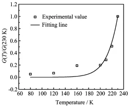
FIG.4 The experimental data and the theoretical ftting curve of Bi nanowires conductance in semiconductor region, all values have been normalized to transition point.

FIG.5 The experimental data and the ftting curve of Bi nanowires conductance in semimetal region,all values have been normalized to transition point.
IV.CONCLUSION
In this study,the single crystal bismuth nanowire arrays grown along[01¯12]with the diameters of 30 nm was synthesized in the AAO templates through electrodeposition process.The temperature dependent electric conductanceG(T)of Bi nanowire arrays was measured. The results show that,for 30 nm Bi nanowires oriented along[01¯12],the semimetal-to-semiconductor transition happens at 230 K and the electric conductance of the nanowires has a strong temperature dependence.In semiconductor region,the conductance of the nanowires increased exponentially with the increase of temperature,while decreased quickly with the increasing temperature in semimetal region.
V.ACKNOWLEDGMENTS
This work was supported by the National Basic Research Program of China(No.2012CB932303), the National Natural Science Foundation of China (No.51171176 and No.11204307),and the CAS/SAFEA International Partnership Program for Creative Research Teams.
[1]T.J.Trentler,K.M.Hickman,S.C.Goel,A.M.Viano, P.C.Gibbons,and W.E.Buhro,Science270,1791 (1995).
[2]W.Wang,C.Xu,G.Wang,Y.Liu,and C.Zheng,J. Appl.Phys.92,2740(2002).
[3]Q.Wu,Z.Hu,X.Wang,Y.Lu,X.Chen,H.Xu,and Y.Chen,J.Am.Chem.Soc.125,10176(2003).
[4]D.G.Cahill,W.K.Ford,K.E.Goodson,G.D.Mahan,A.Ma jumdar,H.J.Maris,R.Merlin,and S.R. Phillpot,J.Appl.Phys.93,793(2003).
[5]D.Routkevitch,A.A.Tager,J.Haruyama,D.Almawlawi,M.Moskovits,and J.M.Xu,IEEE Trans. Electron Devices43,1646(1996).
[6]L.D.Hicks,T.C.Harman,and M.S.Dresselhaus, Appl.Phys.Lett.63,3230(1993).
[7]X.Sun,Z.Zhang,and M.S.Dresselhaus,Appl.Phys. Lett.26,4005(1999).
[8]A.J.Levin,M.R.Black,and M.S.Dresselhaus,Phys. Rev.B79,165117(2009).
[9]J.Heremans,C.M.Thrush,Y.M.Lin,S.Cronin,Z. Zhang,M.S.Dresselhaus,and J.F.Mansfeld,Phys. Rev.B61,2921(2000).
[10]Y.M.Lin,X.Sun,and M.S.Dresselhaus,Phys.Rev. B62,4610(2000).
[11]R.T.Isaacson and G.A.Williams,Phys.Rev.185, 682(1969).
[12]M.P.Vecchi and M.S.Dresselhaus,Phys.Rev.B10, 771(1794).
[13]Z.Zhang,X.Sun,J.Y.Ying,M.S.Dresselhaus,and J.Heremans,Phys.Rev.B61,4850(2000).
[14]C.F.Gallo,B.S.Chandrasekhar,and P.H.Sutter,J. Appl.Phys.34,144(1963).
[15]C.Kittle,Introduction to Solid State Physics,8th Edn., New York:Wiley,(2005).
[16]J.Heremans and O.P.Hansen,J.Phys.C12,3483 (1979).
[17]Y.M.Lin,S.B.Cronin,J.Y.Ying,M.S.Dresselhaus, and J.P.Heremans,Appl.Phys.Lett.76,3944(2000).
10.1063/1674-0068/28/cjcp1409164tion of the morphologies and the structures study,and the other was used for conductance measurement.
∗Author to whom correspondence should be addressed.E-mail:gtfei@issp.ac.cn,Tel.:+86-551-65591453,FAX:+86-551-65591434
(Dated:Received on September 30,2014;Accepted on October 30,2014)
 CHINESE JOURNAL OF CHEMICAL PHYSICS2015年1期
- CHINESE JOURNAL OF CHEMICAL PHYSICS的其它文章
- Nanosecond Rapid Crystallization of Water Induced by Quartz Glass under Dynamic Compression
- Benzene and Toluene Levels Measured with DOAS During Vehicular Restrictions in Beijing
- Antimicrobial Expanded Polytetrafuoroethylene Film Prepared byγ-ray Radiation Induced Grafting of Poly(acrylic acid)
- Aromatic Compounds Production from Sorbitol by Aqueous Catalytic Reforming
- Synthesis of Hierarchically Porous CaFe2O4/Carbon Fiber Hybrids and Microwave Induced Catalytic Activity
- Infuence of Triarylamine and Indoline as Donor on Photovoltaic Performance of Dye-Sensitized Solar Cells Employing Cobalt Redox Shuttle