
High Performance of Enhanced Mode Field Efect Transistor and Ultraviolet Sensor Based on ZnO Nanosheet
2015-01-13 02:25:32ZhiweiGaoYukunWuJunwenLiXiaopingWang
Zhi-wei GaoYu-kun WuJun-wen LiXiao-ping Wang
Department of Physics,University of Science and Technology of China,Hefei 230026,China
High Performance of Enhanced Mode Field Efect Transistor and Ultraviolet Sensor Based on ZnO Nanosheet
Zhi-wei Gao,Yu-kun Wu,Jun-wen Li,Xiao-ping Wang∗
Department of Physics,University of Science and Technology of China,Hefei 230026,China
ZnO nanosheets with thickness of a few nanometers are prepared by vapor transport and condensation method,and their structure and optical properties are well characterized. Field efect transistor(FET)and ultraviolet(UV)sensors are fabricated based on the ZnO nanosheets.Due to the peculiar structure of nanosheet,the FET shows n-type enhanced mode behavior and high electrical performance,and its feld-efect mobility and on/of current ratio can reach 256 cm2/(V·s)and~108,respectively.Moreover,the response of UV sensors can also be remarkably improved to~3×10⁸.The results make the ZnO nanosheets be a good material for the applications in nanoelectronic and optoelectronic devices.
ZnO,Nanosheets,Field efect transistor,UV sensor
I.INTRODUCTION
ZnO,as a wide-gap semiconductor with large exciton binding energy of 60 meV,has widely potential applications for laser[1],feld efect transistor(FET) [2],UV sensor[3],light-emitting device[4],piezotronics[5],solar cells[6],spintronics[7,8]and transparent and fexible electronics[9].So far,most of FET and UV sensor based on ZnO materials are constructed with ZnO nanowires.Unfortunately,due to abundant intrinsic n-type defects,even undoped ZnO nanowire has a high initial carrier concentration.This results in inevitably the high of-state current for ZnO nanowire FET because it is difcult to deplete the carriers completely in the conducting nanowire channel with diameter of several hundred nanometers[10].Although the problem can be alleviated by using the nanowires with small diameter,the on-state current of the device also decreases simultaneously,failing to be used for logic circuit.Moreover,as the diameter of nanowires shrinks, the abundant surface scattering can degrade dramatically the carrier mobility of nanowire.In this regard,it is a challenge to design and fabricate ZnO nanostructure FET with both high on-of current ratio and carrier mobility performances.
Herein,we suppose to use thin ZnO nanosheet with thickness down to a few nanometers rather than ZnO nanowire for fabrication of FET.We fnd that the ZnO nanosheet FET can not only show ultralow of-state current due to the strong depletion formed under the surface,but also run much higher on-state current than the nanowire device,resulting in excellent on-of current ratio as high as 108.In addition,even the thickness of nanosheet is as thin as several nanometers,the feldefect mobility of FET device can reach 256 cm2/(V·s). The result is even better than that of the bulk ZnO. More importantly,the FET device exhibits n-type enhanced mode,which typically has positive threshold voltage and operates with of-state current at zero gate bias.Consequently,the enhanced mode devices are more preferable for the low power consumption,simply integration circuit design and accurate charge carriers modulation[11].Moreover,the UV sensor with ultrahigh photo-responsivity can be realized based on the ZnO nanosheet.All the results demonstrate that the ZnO thin nanosheets can be used as an excellent alternate material for nanoelectronic and optoelectronic devices.
II.EXPERIMENTS
ZnO nanosheets were synthesized via vapor transport and condensation method by using 5 nm Ag flm as substrates[12,13].The source,composed of 0.5 g uniform mixtures(1∶1 mole ratio)of ZnO powders(purity~99.99%)to spectrograde graphite powders,was located in one sealed end of quartz tube with length of 27 cm and inner diameter of 1.5 cm,whereas the Si(111) substrate coated by 5 nm Ag flm was located near the other open end of the tube.The distance between the source and the substrate was about 22 cm.The quartz tube was then put into furnace and ensured the source to sit at high temperature(HT)zone of the furnace while the substrate sit at low temperature(LT)zone. Ar(20 sccm)was used as the carrier gas in all reaction process.The HT zone was heated up to 1000◦C in
The morphologies of the ZnO nanosheets were characterized by JEOL-6700 feld-emission scanning electron microscope(FE-SEM)and Seiko SPA-300HV atomic force microscopy(AFM).The crystalline structure of the nanosheet was analyzed by PHILIPS X’PERT PRO X-ray difractometer(XRD)with Cu Kαline(λ=1.54184˚A).The high resolution transmission electron microscopy(HRTEM)image of ZnO nanosheets was obtained with JJEM-ARM200F operated at 200 kV.The optical properties of nanosheets were checked by LABRAM-HR Raman spectrometer with excitation wavelength of 325 nm.The fabrication of FET and/or UV sensor includes the following processes.First,polydimethylsiloxane(PDMS)was used as a stamp to transfer the as-grown ZnO nanosheets to a degenerately p-doped silicon wafer covered with 300 nm thick SiO2.Subsequently,the electrodes of 10 nm Ti/100 nm Au were patterned to the nanosheet by e-beam lithography,metal deposition and lift-of processing[14].The characteristics of the devices were investigated by Keithley 4200 combined with Lake Shore CRX-4K probe station.

FIG.1(a)SEM image of ZnO nanosheets.(b)High magnifcation SEM image of ZnO nanosheets.

FIG.2(a)XRD pattern of ZnO nanosheets.(b)PL spectrum of ZnO nanosheets under excitation at 325 nm.
III.RESULTS AND DISCUSSION
Figure 1(a)is the SEM result of the as-grown ZnO nanosheets.As seen,the nanosheets are formed on the substrate with uniform distribution.From the zoom in SEM in Fig.1(b),we can estimate that the averaged width and length of the nanosheet are about 2 and 10µm respectively,while the thickness is about several nanometers.The XRD result of the as-grown ZnO nanosheets shown in Fig.2(a)is consistent well with JCPDS card No.36-1451,indicating the nanosheet with a wurtzite ZnO structure.Figure 2(b)is the photoluminescence results of ZnO nanosheet.The peak located at 379 nm is the near-band-edge(NBE)emission of ZnO while the peak at 758 nm is its overtone.The broad luminescence with the peak located at 650 nm is similar to the result of the un-doped ZnO,which is considered to be related to the defects emission(DE)of ZnO[15]. Note that the intensity of NBE is much stronger than that of DE,implying good crystalline of the nanosheet.
The morphology and thickness of ZnO nanosheet are characterized by AFM and the typical result is shown in Fig.3(a).As seen,the surface morphology of the ZnO nanosheet is uniform and the height profle line in inset of Fig.3(a)reveals its thickness about 8 nm. TEM characterization is also carried out to investigate the microstructure of ZnO nanosheets and the result is depicted in Fig.3(b).Both HRTEM image and selected area electron difraction(SAED)pattern shown in Fig.3(c)demonstrate that the ZnO nanosheet is single crystalline with wurtzite structure.Moreover,it is found that the nanosheet has strong preference to grow along both of〈0001〉and〈01-10〉directions.Consequently,the top/bottom surfaces of the ZnO nanosheet belong to±(2-1-10)plane,while the sides are composed of±(0001)and±(01-10)planes,as illustrated in Fig.3(d).
In order to investigate the electrical properties of ZnO nanosheet,we fabricated the ZnO nanosheet FET and measured its transfer performance under air and vacuum environment respectively.As shown in Fig.4(a), under the air and with the source-drain voltage ofVDS=50 mV,the transfer characteristic(triangle curve) of FET demonstrates excellent ability of gate modula-tion.The of-state source-drain currentIDScan reach as small as 10−13A,while the on-state current is about 10−5A,resulting in ultrahigh on-of current ratio~108. This value is three orders of magnitude larger than previously reported nanostructure ZnO FET[2].Figure 4(b)shows theI-Vcurves of the device under air with diferent gate voltages.The linear behavior of the curve implies the well electrical contact between the electrodes and the nanosheet.At the same time,the strong gate modulation can also be found.Moreover, the fled efect mobility(µFE)of the FET device can be obtained from the transfer characteristics according to the following equation[16]∶

FIG.3(a)Topographical AFM image of ZnO nanosheet. Inset is the height profle line.(b)TEM image of ZnO nanosheet.(c)HRTEM image and SAED pattern(inset)of ZnO nanosheet.(d)Structure illustration of ZnO nanosheet.

FIG.4(a)Semilogarithmic and linear(inset)plots of transfer characteristics of ZnO nanosheet FET under air and vacuum with UV irradiation.(b)TypicalI-Vcharacteristic of ZnO nanosheet FET under air at diferent gate voltages.
whereCG,gm,Ls,andWsare the gate capacitance, transconductance,the channel length,and width of the FET,respectively.With our device,for 300 nm thick SiO2,CG=11.505 nF/cm2,gm=1.47×10−7S atVDS=50 mV,Ls=3µm andWs=3µm.Therefore,µFEis estimated to be 256 cm2/(V·s),which is even slightly better than that of the bulk ZnO(~200 cm2/(V·s)[17]. Considering that the carriers could sufer severe surface scattering in the nanosheet,the obtained high mobility in the nanosheet is rather an amazing result.This defnitely implies the high quality of crystallinity and the fat surface of the nanosheet,but the underlying reason might also be related to the formation of quasitwo-dimensional electron gas in the nanosheet,which is needed for the further study.

To better understand the above consideration,we carried out a control experiment for the FET device. The absorbed molecules on the surface of FET were removed through the irradiation of ultraviolet lamp for 4 h in high vacuum.Afterwards,the transfer characteristic of the device was measured again.The result is plotted in Fig.4(a)(square curve).As seen,the device does not demonstrate of-state during the gate voltage varying in range between±50 V,and the source-drain current can only change a factor of less than 10,indi-cating the weak gate modulation to the device.With the aforementioned method,we can also calculate the mobility of the device~260 cm2/(V·s),similar to the value obtained from the device in the air ambience.The result is reasonable because the mobility is an intrinsic character of the material and susceptive to the defects only.
Withσ=neµ,we further estimate the intrinsic electron density of the nanosheet to be 5×1018cm−3,indicating the as-grown ZnO nanosheet is in heavy doping. It has been reported that the inevitably intrinsic defects of ZnO,such as oxygen vacancy(VO)or zinc interstitial(Zni)can contribute to the electron carriers[19, 20].Therefore,we speculate that there exist many intrinsic defects in ZnO nanosheet.This consideration is also supported by the red luminescence behavior shown in Fig.2(b).It has be pointed out that the conductance of ZnO nanostructure decreases in air ambience, because the absorbed molecules can trap the electrons in ZnO and form a depletion layer under the surface. The thickness of depletion layerWcan be estimated by [21]∶
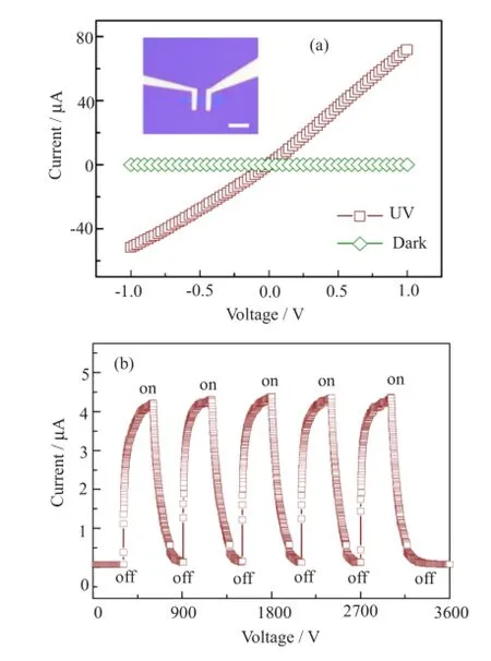
FIG.5(a)UV response of ZnO nanosheet device.Inset:optical photo of the device.The bar is 5µm.(b)Current response versus time under periodic UV irradiation.
wheree,ND,ε0,εZnO,andϕsare the electron charge,the doping density,the vacuum permittivity,the relative static permittivity of ZnO,and the surface barrier potential,respectively.AssumingND=1018cm−3,ϕs=0.3 V,andεZnO=8.66[22],we can obtainW≈17 nm.Obviously,although this depletion layer has negligible efect on the conductance for the ZnO nanostructures with several hundred nanometers of lateral size,it can result in complete depletion in the few nanometers thick ZnO nanosheet and lead to the enhanced mode behavior of FET.
Considering that strong depletion layer exists in ZnO nanosheet and the adsorbed molecules can be removed through the UV irradiation,we believe the nanosheet is very adaptable to construct UV sensor.Figure 5(a)shows theI-Vcurves of the ZnO nanosheet sensor device with and without irradiation of ultraviolet light(central length at 365 nm with a power density of 500µW/cm2).The inset is the optical image of the fabricated sensor.The photo-responsivity of the sensor,defned as the ratio of the current under irradiation to that in the dark,can reach as large as~3×10⁸under the bias voltage of 1 V.This high photoresponsivity comes from not only high photocurrent (7.2×10⁻⁵A atVDS=1 V)but also extremely low dark current(2.8×10⁻¹³A atVDS=1 V).High photocurrent origins dominantly from the released carriers captured by absorbed molecules under UV irradiation[23].Figure 5(b)shows the photocurrent response of the sensor at bias of 50 mV under on/of periodic UV irradiation. As seen,the response of the device to the UV irradiation is quite well,and the response time is less than 5 s and the recovery time is about 60 s.
IV.CONCLUSION
ZnO nanosheets with thickness down to a few nanometers are grown by vapor transport and condensation method.The nanosheet is single crystalline with wurtzite structure.The top/bottom surfaces of ZnO nanosheet belong to±(2-1-10)plane,and the sides are composed of±(0001)and±(01-10)planes.The FET fabricated by the ZnO nanosheet shows n-type enhanced mode behavior and high gate modulation performance.The mobility of device is about 256 cm2/V·s and the on/of current ratio can reach 108.Additionally,the photo-responsivity of the nanosheet UV sensor can also be dramatically improved to 3×10⁸.Our fndings indicate that the well controlled grown thin ZnO nanosheet can be used as an excellent material to construct the high performance nanoelectronic and optoelectronic devices.
V.ACKNOWLEDGMENTS
This work was supported by Ministry of Science and Technology of China(No.2011CB921403),the National Natural Science of Foundation of China(No.11374274 and No.11074231),and Chinese Academy of Science (No.XDB01020000).
[1]M.H.Huang,S.Mao,H.Feick,H.Yan,Y.Wu,H. Kind,E.Weber,R.Russo,and P.Yang,Science292, 1897(2001).
[2]P.C.Chang,Z.Fan,C.J.Chien,D.Stichtenoth,C. Ronning,and J.G.Lu,Appl.Phys.Lett.89,133113 (2006).
[3]J.Y.Liu,X.X.Yu,G.H.Zhang,Y.K.Wu,K.Zhang, N.Pan,and X.P.Wang,Chin.J.Chem.Phys.26,225 (2013).
[4]A.Tsukazaki,A.Ohtomo,T.Onuma,M.Ohtani,T. Makino,M.Sumiya,K.Ohtani,S.F.Chichibu,S.Fuke, Y.Segawa,H.Ohno,H.Koinuma,and M.Kawasaki, Nat.Mater.4,42(2005).
[5]Z.L.Wang and J.H.Song,Science312,242(2006).
[6]M.Law,L.E.Greene,J.C.Johnson,R.Saykally,and P.Yang,Nat.Mater.4,455(2005).
[7]T.Dietl,H.Ohno,F.Matsukura,J.Cibert,and D. Ferrand,Science287,1019(2000).
[8]S.H.Deng,M.Xu,M.Y.Duan,and O.Brian,Chin. J.Chem.Phys.26,303(2013).
[9]S.H.Kim,J.Yoon,S.O.Yun,Y.Hwang,H.S.Jang, and H.C.Ko,Adv.Funct.Mater.23,1375(2013).
[10]J.Zhou,Y.Gu,Y.Hu,W.Mai,P.H.Yeh,G.Bao, A.K.Sood,D.L.Polla,and Z.L.Wang,Appl.Phys. Lett.94,(2009).
[11]B.Radisavljevic,A.Radenovic,J.Brivio,V.Giacometti,and A.Kis,Nat.Nano6,147(2011).
[12]G.Z.Xing,X.S.Fang,Z.Zhang,D.D.Wang,X. Huang,J.Guo,L.Liao,Z.Zheng,H.R.Xu,T.Yu,Z. X.Shen,C.H.A.Huan,T.C.Sum,H.Zhang,and T. Wu,Nanotechnology21,255701(2010).
[13]Z.W.Gao,Y.Lin,J.W.Li,and X.P.Wang,Chin.J. Chem.Phys.27,350(2014).
[14]Y.Cheng,P.Xiong,L.Fields,J.P.Zheng,R.S.Yang, and Z.L.Wang,Appl.Phys.Lett.89,093114(2006). [15]A.B.Djuri˘si´c,W.C.H.Choy,V.A.L.Roy,Y.H. Leung,C.Y.Kwong,K.W.Cheah,T.K.G.Rao,W. K.Chan,H.F.Lui,and C.Surya,Adv.Funct.Mater.14,856(2004).
[16]L.Liao,J.Bai,Y.Qu,Y.C.Lin,Y.Li,Y.Huang,and X.Duan,Proc.Natl.Acad.Sci.107,6711(2010).
[17]D.C.Look,D.C.Reynolds,J.R.Sizelove,R.L.Jones, C.W.Litton,G.Cantwell,and W.C.Harsch,Solid State Commun.105,399(1998).
[18]X.Li,X.Wang,L.Zhang,S.Lee,and H.Dai,Science319,1229(2008).
[19]D.C.Look,J.W.Hemsky,and J.R.Sizelove,Phys. Rev.Lett.82,2552(1999).
[20]S.B.Zhang,S.H.Wei,and A.Zunger,Phys.Rev.B63,075205(2001).
[21]W.K.Hong,J.I.Sohn,D.K.Hwang,S.S.Kwon,G. Jo,S.Song,S.M.Kim,H J.Ko,S.J.Park,M.E. Welland,and T.Lee,Nano Lett.8,950(2008).
[22]Z.Fan and J.G.Lu,J.Nanosci.Nanotechnol.5,1561 (2005).
[23]Y.Hu,Y.Liu,W.Li,M.Gao,X.Liang,Q.Li,and L. M.Peng,Adv.Funct.Mater.19,2380(2009).
10.1063/1674-0068/28/cjcp141017748 min,and then the LT zone was heated up to 550◦C in 6 min.Once the temperature of LT zone reached 550◦C,O2(10 sccm)was introduced and lasted for 10 min,then the heat power of two-zone furnace and O2fow were shut down.The furnace was cooled down to room temperature naturally under Ar gas protection.
∗Author to whom correspondence should be addressed.E-mail:xpwang@ustc.edu.cn
(Dated:Received on October 13,2014;Accepted on October 23,2014)
 CHINESE JOURNAL OF CHEMICAL PHYSICS2015年1期
- CHINESE JOURNAL OF CHEMICAL PHYSICS的其它文章
- Nanosecond Rapid Crystallization of Water Induced by Quartz Glass under Dynamic Compression
- Benzene and Toluene Levels Measured with DOAS During Vehicular Restrictions in Beijing
- Antimicrobial Expanded Polytetrafuoroethylene Film Prepared byγ-ray Radiation Induced Grafting of Poly(acrylic acid)
- Aromatic Compounds Production from Sorbitol by Aqueous Catalytic Reforming
- Synthesis of Hierarchically Porous CaFe2O4/Carbon Fiber Hybrids and Microwave Induced Catalytic Activity
- Infuence of Triarylamine and Indoline as Donor on Photovoltaic Performance of Dye-Sensitized Solar Cells Employing Cobalt Redox Shuttle