Zn xCd1-xS纳米线的可控合成及其可调的光学性质
林旭锋 席燕燕 林德莲
(1中国石油大学(华东)重质油国家重点实验室,山东青岛 266580;2中国石油大学(华东)理学院,山东青岛 266580;3中国石油大学(华东)化工学院,山东青岛 266580)
1 Introduction
One dimensional semiconductor micro and nano structures have attracted much attention due to their novel properties and potential applications in many fields such as lasers,1-3waveguides,4and optical switches.5For devices in nanoelectronics and nanophotonics,it is very important to fabricate materials with continuous tunable physical properties.Band gap energy is one of the most important parameters that characterize a semiconductor and determine many gross electronic and optical properties.In the past few decades,extensive attention has been devoted to tuning the band gap energy of the nanowires by means of reducing its size to values comparable with or smaller than the corresponding excitonic Bohr diameter.6-10However,progress in this field only gives the ability to generate nanowires with diameters in a limited range,in which the quantum confinement effect is not prominent.
Alloying of semiconductors is another means that can be applied to achieve semiconductor materials with various band gap energies.Alloy nanostructures of ternary II-VI semiconductors with elementary composition of ZnCdSe,ZnCdS,and CdSSe have been successfully fabricated by metal organic chemical vapor deposition(MOCVD),11-14electrodeposition,15laser-assisted deposition16,17and microwave-assisted synthesis.18,19They present high luminescence nature and well-crystalline structures and have been demonstrated to possess high lasing efficiency in a broad range of compositions.16In recent years,remarkable progress in the growth processes of nanocrystals has put alloy materials(III-V,II-VI)and their technology in a special category that promises versatile applications in photonic,13,20-22and high efficiency photovoltaic23devices.
ZnxCd1-xS,whose physical and chemical properties can be tuned by changing the constituent stoichiometries,24,25is a good candidate to offer flexible physical parameters suitable for advanced application in nanotechnology.In a previous work26we have reported that Zn0.88Cd0.12S nanowires were synthesized by a simple vapor deposition method in ambient and lower pressures.The nanowires synthesized under ambient pressure grow along the<0001> directions via the tip-growth vapor-liquid-solid(VLS)mechanism.The nanowires synthesized under~1.33×10⁴Pa grow along the<1010> direction via the combined basegrowth VLS and tip-growth vapor-solid(VS)mechanism.
In this context several interesting questions became open.Firstly,whether or not can the ZnxCd1-xS nanowire be synthesized with tunable x value by this vapor deposition mechanism?Secondly,what are the growth mechanisms?Thirdly,whether does this tunable x value bring tunable physical,especially optical,properties.In this work we aim at answering these questions.
2 Experimental
2.1 Synthesis of ternary Zn xCd1-xS powder
The ternary ZnxCd1-xS powder was prepared before the preparation of its nanowire.The powder was synthesized based on the work of Rincon et al.27Two grams of CdS powder(99.5%,International Laboratory,USA)and 0.94 g of ZnCl2powder(A.R.Fisher Scientific,UK)were mixed and put into an alumina boat.The boat was placed in the center of an alumina tube before it was inserted in a horizontal tube furnace.The mixture was sintered at 450°C for 12 h in an argon atmosphere.The possible reactions during sintering were:

If the reactions were complete,the sintered product contained ZnxCd1-xS and CdCl2.
2.2 Synthesis of Zn xCd1-xS nanowires
Then the as-prepared powder was ground and put into an alumina boat,which was then placed in the center of a quartz tube.The entire assembly was inserted in a horizontal tube furnace.The system was connected to an argon source and a rotary pump.The system was evacuated before a steady Ar flow(at a rate of 60 cm3·min-1)was introduced.The temperature of the furnace was ramped to 900°C and held for 100 min.Several Au-coated Si(100)wafers were placed on the downstream side at the different positions of the quartz tube and separately about 2-18 cm from the source material.Colors for the as-synthesized products vary from white(ZnS)to yellow(CdS)depending on the composition(x value).It is found that the ZnxCd1-xS nanowires of various compositions were deposited at different collection positions,that is,at distinctive deposition temperature.CdCl2which has a lower melting point(576°C)and boiling point(950°C)could evaporate at such a temperature.
2.3 Characterization
The crystalline structure of the product was characterized by X-ray diffractometry(XRD,Rigaku RU-300).The microstructural analyses were performed by using scanning electron microscopy(SEM,LEO 1450 VP),transmission electron microscopy(TEM,Philips Tecnai 20),and high-resolution TEM(HRTEM,Philips Tecnai 20).Elemental and composition analyses were carried out by using energy dispersive X-ray spectrometry(EDX,Oxford Link II,UK).The optical properties were studied by Raman spectroscopy(Renishaw,Rm,1000B,excitation line of 514.5 nm)and photoluminescence(PL,Renishaw,Rm,1000B,excitation line of 325 nm).
3 Results and discussion
3.1 Morphology and composition
General SEM morphologies of the as-synthesized ZnxCd1-xS nanowires orienting randomly on the Si substrate are shown in Fig.1(a,c,e,g)with x=0.13,0.31,0.68,0.88(indicated in Fig.1(b,d,f,h)),respectively.The lengths of the wires are up to~100µm,and the diameters of the ZnxCd1-xS nanowires are distributed in the range of 200-350 nm.The samples synthesized at a lower deposition temperature have smaller size.Chemical contents of the ZnxCd1-xS nanowires analyzed from EDX data with their stoichiometric ratios are listed in Table 1.It can be seen that for all samples with different compositions,the atomic ratio of S is smaller than 50%,which indicates the existence of the defect in the as-synthesized ZnxCd1-xS nanowires.
3.2 Crystal structure
It is known that for some common ternary compounds,the relationship between the composition value x and the lattice parameters along the c-axis follows the Vegardʹs law.28-30Based on the Vegardʹs law,the lattice constants along the c-axis of ZnS,CdS,and ZnxCd1-xS crystals,denoted as cZnS,cCdS,and cx,respectively,are subjected to the following equation:


Fig.1 SEM images of the Zn xCd1-xS nanowires(a,c,e,g)and their corresponding EDS spectra(b,d,f,h)x:(a,b)0.13,(c,d)0.31,(e,f)0.68,(g,h)0.88

Table 1 Chemical compositions of the Zn xCd1-xS nanowires measured by EDX
Fig.2 displays typical XRD patterns of the ZnxCd1-xS nanowires synthesized at different conditions.The XRD patterns show that the nanowires with different compositions all have the hexagonal wurtzite structure.The corresponding x values of the nanowires calculated by Vigardʹs law were indicated at the right of the curves in Fig.2.For the calculation of the x value,the peaks for the(002)and(101)planes were used,which for ZnS lie at 2θof~28.5°and ~30.6°,respectively,and for CdS at 2θof~26.5°and ~28.2°,respectively.As a result,the positions of the(002)peak in XRD patterns shift from 26.5°to 26.7°,27.1°,27.8°,28.2°,and 28.5°as the fraction of Zn(x)in ZnxCd1-xS increases from 0 to 0.13,0.31,0.68,0.88,and 1.00,respectively.The calculated x values of the ZnxCd1-xS nanowires with x=0.13,0.31,0.68,0.88 are well consistent with those from the EDX results.
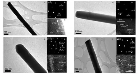
Typical TEM images of the as-synthesized ZnxCd1-xS nanowires with x=0.13,0.31,0.68,0.88 are shown in Fig.3(a,d,g,j),respectively.The selected area electron diffractions(SAED,Fig.3(b,e,h,k))and HRTEM(Fig.3(c,f,i,l))images are correspondingly attached to the TEM images.The SAED and HRTEM images further reveal that the synthesized ZnxCd1-xS nanowires are single crystalline and have hexagonal Wurtzite structure.Lattice constants,growth directions,and lattice spacings calculated from the HRTEM and XRD data are listed in Table 2.Consistently,the lattice constants determined from the SAED data are in good agreement with the XRD results.

Fig.2 XRD patterns of the Zn xCd1-xS nanowires obtained at different deposition conditions
3.3 Discussion on the growth mechanism
There are two well-accepted mechanism for the growth of one dimesional(1D)nanostructures,viz.the vapor-solid(VS)and the vapor-liquid-solid(VLS)mechanisms.For nanowires growing through the VS mechanism,there always has a decrease of the diameter/width of the nanostructures toward their growth end.31,32The VLS mechanism can be divided into two types,viz.tip-growth VLS mechanism and base-growth mechanism.The existence of a metal-alloy droplet on the tip of the 1D nanostructure is the characteristic of the former.31,33,34For the later,an Au nanoparticle may stay at the bottom of the nanowires during the growth process.31,35In this work,the alloy droplet on the tip of the nanowires was not observed(see Fig.3),which indicates that the tip-growth VLS mechanism is not appropriate.Meanwhile,the diameters of the nanowires are rather uniform along the growth direction,except for the case of x=0.68 which is a little cuspidal.Thus the results support that the base-growth mechanism is plausible for the ZnxCd1-xS nanowire growth in our preparation method.

Fig.3 TEM(a,d,g,j),SAED(b,e,h,k),and HRTEM(c,f,i,l)images of the as-synthesized Zn0.13Cd0.87S(a,b,c),Zn0.31Cd0.69S(d,e,f),Zn0.68Cd0.32S(g,h,i),and Zn0.88Cd0.12S(j,k,l)nanowires

Table 2 Lattice spacings,growth directions,and lattice constants in the Zn xCd1-xS nanowires
3.4 Optical properties
3.4.1 Raman study
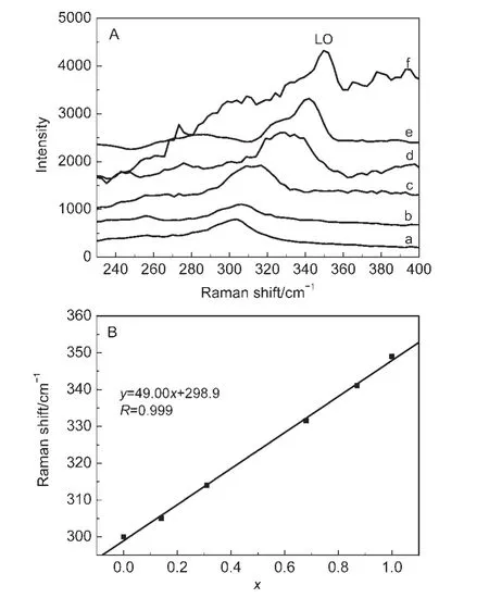
For the phonons in a mixed crystal of ternary alloys,a modified random element isodisplacement(MREI)model developed by Chan and Mitra36suggests that the criterion for the existence of the one-mode pattern is that there must not be a substituting element whose mass(m)is smaller than the reduced mass(μ)of the compound formed by the other two elements.In the ternary alloy of ZnxCd1-xS,since mCd(=112)>μZnS(=21)and mZn(=64)>μCdS(=25),one mode behavior should be exhibited for the phonons in the ZnxCd1-xS mixed crystal according to the MREI model.It was reported for the ZnxCd1-xS thin film that both cubic and hexagonal ZnxCd1-xS exhibit the one mode behavior,i.e.,one dominant longitudinal optical(LO)phonon peak is observed and its frequency changes smoothly with composition between those two constituent compounds.37,38
Fig.4A depicts the Raman spectra of the ZnxCd1-xS nano-wires with different compositions.The Raman shifts at 300 and 345 cm-1are attributed to the LO phonon modes of CdS and ZnS,respectively.These phonon frequencies of LO modes agree well with the present observations.15,39In Fig.4A,phonon frequency(proportional to Raman shift)for the LO mode in the ZnxCd1-xS nanowires increases as the Cd composition decreases.Fig.4B shows the variation of the Raman shifts for the LO mode as a function of x value in the ZnxCd1-xS nanowires.The Raman shifts vary continuously and linearly with the variation of the x value,and once more exhibit roughly the one-mode behavior pattern.
3.4.2 Photoluminescence study

Fig.4 (A)Raman spectra of the Zn xCd1-xS nanowires with different compositions,with(a)CdS,(b)Zn0.13Cd0.87S,(c)Zn0.31Cd0.68S,(d)Zn0.68Cd0.32S,(e)Zn0.88Cd0.12S,(f)ZnS;(B)the composition dependence of the Raman shifts for the LO vibrational mode of the Zn xCd1-xS nanowires
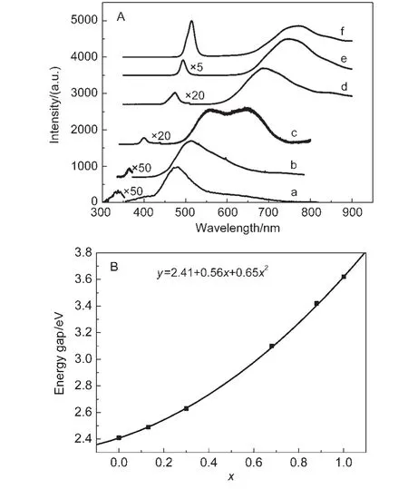
Good optical properties are always desired for applications in optoelectronic devices.PL measurements were carried out to characterize the optical properties of the alloy nanowires.Strong emission was found in our experiments from these nanowires.Fig.5A shows the normalized PL spectra of the ZnxCd1-xS nanowires of x=0,0.13,0.31,0.68,0.88,1.00.The x values were calculated from the results of EDX and XRD.Two emission bands were obtained for the wires with all compositions.The one located at the higher energy region is attributed to the near-band-edge(NBE)emission and the other one located at the lower energy region is assigned to the defect-related emission band.The full widths at half-maximum(FWHM)of the NBE PL for these nanowires are 15-20 nm,which is comparable to those of the widely used II-VI spherical quantum dots.40,41Such narrow peaks of the band-edge fluorescent emission imply that the distribution of the composition in these nanowires is quite uniform.Meanwhile,it was also found that the increase of the Cd ratio in the ZnxCd1-xS nanowires leads to the increased PL intensity originating from the increases of band-gap transition,in contrast to the decreased PL intensity originating from the defects.
Meanwhile,a distinct blue shift of the NBE peak can be seen with increasing Zn composition.The peaks of the NBE emission change from ~340 nm(pure ZnS)to ~515 nm(pure CdS)as the Cd ratio increases.Energy gaps for the ZnxCd1-xS nanowires calculated from the observed PL peaks are shown in Fig.5B as a function of x value.Variation of the energy gaps deviates slightly from linear dependence,displaying a downward bowing,which has also been reported as a general character for many thin films of II-VI alloy semiconductors42,43and 1D nanostructures.15,17The nonlinear variation of the energy gaps can be represented as a function of composition

Fig.5 (A)PL spectra of the Zn xCd1-xS nanowires with different compositions,with(a)ZnS,(b)Zn0.13Cd0.87S,(c)Zn0.31Cd0.68S,(d)Zn0.68Cd0.32S,(e)Zn0.88Cd0.12S,(f)CdS;(B)the composition dependence of the energy gap of the Zn xCd1-xS nanowires

where Eg(x)is the energy gap of the AxB1-xC alloy crystal,EACand EBCare the energy gaps of the end-member crystals of AC and BC,respectively,and b is the bowing parameter.In this work,from the Egdata deduced from the PL spectra of the ZnxCd1-xS nanowires,the relationship between Egand x value can be written as:

From Eq.(5)the bowing parameter b is calculated to be 0.65 eV.The PL results show that the band-gap energy of the ZnxCd1-xS nanowires can be continuously tuned from 2.41 to 3.63 eV.With broadly tunable optical properties and electrical properties,these alloyed nanowires can be used in colortuned nanolasers,biological labels,and nanoelectronics.
4 Conclusions
In summary,we have successfully synthesized the ZnxCd1-xS nanowires with single crystal via a simple vapor deposition method with varying compositions.The compositions determined by EDX and XRD are in good consistence.The XRD,HRTEM,and SAED results show that the as-synthesized nanowires are highly single crystalline.Raman measurements for the LO phonon in the ZnxCd1-xS nanowires show that the phonon frequency shifts linearly with the composition.The PL results show that the NBE emission band of the ZnxCd1-xS nanowires can be tuned from 2.41 eV(CdS)to 3.63 eV(ZnS)and this indicates that we have achieved continuous band-gap tuning through composition modulation in highly crystalline ZnxCd1-xS nanowires.
(1)Huang,M.H.;Mao,S.;Feick,H.;Yan,H.Q.;Wu,Y.Y.;Kind,H.;Weber,E.;Russo,R.;Yang,P.D.Science 2001,292,1897.doi:10.1126/science.1060367
(2)Bando,K.;Sawabe,T.;Asaka,K.;Masumoto,Y.J.Lumin.2004,108,385.doi:10.1016/j.jlumin.2004.01.081
(3)Hu,C.;Zeng,X.H.;Cui,J.Y.;Chen,H.T.;Lu,J.F.J.Phys.Chem.C 2013,117,20998.doi:10.1021/jp407272u
(4)Duan,X.;Hu,Y.;Agarwal,R.;Lieber,C.M.Nature 2003,421,24.
(5)Kind,Y.H.;Messer,B.;Law,M.;Yang,P.D.Adv.Mater.2002,14,158.
(7)Gudiksen,M.S.;Lieber,C.M.J.Am.Chem.Soc.2000,122,8801.doi:10.1021/ja002008e
(8)Gudiksen,M.S.;Wang,J.;Lieber,C.M.J.Phys.Chem.B 2002,106,4036.doi:10.1021/jp014392n
(9)Ma,D.D.D.;Lee,C.S.;Au,F.C.K.;Tong,S.Y.;Lee,S.T.Science 2003,299,1874.doi:10.1126/science.1080313
(10)Peng,K.Q.;Wang,X.;Li,L.;Hu,Y.;Lee,S.T.Nano Today 2013,8,75.doi:10.1016/j.nantod.2012.12.009
(11)Shan,C.X.;Liu,Z.;Ng,C.M.;Hark,S.K.Appl.Phys.Lett.2005,87,033108.doi:10.1063/1.1997271
(12)Zhang,X.T.;Liu,Z.;Liu,Q.;Hark,S.K.J.Phys.Chem.B 2005,109,17913.doi:10.1021/jp0527406
(13)Averin,S.V.;Kuznetsov,P.I.;Zhitov,V.A.;Alkeev,N.V.;Kotov,V.M.;Zakharov,L.Y.;Gladysheva,N.B.Tech.Phys.2012,82,49.
(14)Hou,J.W.;Song,B.;Zhang,Z.H.;Wang,W.J.;Wu,R.;Sun,Y.F.;Zheng,Y.F.;Ding,P.;Jian,J.K.Acta Physico-Chimica Sinica 2009,25,724.[侯军伟,宋 波,张志华,王文军,吴 荣,孙言飞,郑毓峰,丁 芃,简基康.物理化学学报,2009,25,724.]doi:10.3866/PKU.WHXB20090428
(15)Liang,Y.Q.;Zhai,L.;Zhao,X.S.;Xu,D.S.J.Phys.Chem.B 2005,109,7120.doi:10.1021/jp045566e
(16)Liu,Y.;Zapien,J.A.;Shan,Y.Y.;Geng,C.Y.;Lee,C.S.;Lee,S.T.Adv.Mater.2005,17,1372.
(17)Venugopal,R.;Lin,P.I.;Chen,Y.T.J.Phys.Chem.B 2006,110,11691.doi:10.1021/jp056892c
(18)Wu,H.;Yao,Y.;Li,W.;Zhu,L.;Ni,N.;Zhang,X.J.Nanopart.Res.2011,13,2225.doi:10.1007/s11051-010-9981-7
(19)Mahdi,M.A.;Hassan,J.J.;Hassan,Z.;Ng,S.S.Journal of Alloys and Compounds 2012,541,227.doi:10.1016/j.jallcom.2012.05.123
(20)Huang,Y.;Duan,X.F.;Lieber,C.M.Small 2005,1,142.
(21)Mcalpine,C.M.;Friedman,R.S.;Lieber,C.M.Proc.IEEE 2005,93,1357.doi:10.1109/JPROC.2005.850308
(22)Sirbuly,D.J.;Law,M.;Yan,H.Q.;Yang,P.D.J.Phys.Chem.B 2005,109,15190.doi:10.1021/jp051813i
(23)Law,M.;Greene,L.E.;Johnson,J.C.;Saykally,R.;Yang,P.D.Nat.Mater.2005,4,455.doi:10.1038/nmat1387
(24)Bailey,R.E.;Nie,S.J.Am.Chem.Soc.2003,125,7100.doi:10.1021/ja035000o
(25)Wei,H.;Ren,X.L.;Han,Z.Y.;Li,T.T.;Su,Y.J.;Wei,L.M.;Cong,F.S.;Zhang,Y.F.Mater.Lett.2013,102,94
(26)Xi,Y.Y.;Cheung,T.L.Y.;Ng,D.H.L.Mater.Lett.2008,62,128.doi:10.1016/j.matlet.2007.04.094
(27)Rincon,M.E.;Martinez,M.W.;Miranda-Hernandez,M.Solar Energy Materials&Solar Cells 2003,77,25.doi:10.1016/S0927-0248(02)00242-8
(28)Sainova,D.S.;Zen,A.;Nothofer,H.H.;Asawapirom,U.;Scherf,U.;Hagen,R.;Bieringer,T.;Kostromine,S.;Neher,D.Adv.Funct.Mater.2002,12,49.doi:10.1002/1616-3028(20020101)12:1<49::AID-ADFM49>3.0.CO;2-D
(29)Ballentyne,D.W.G.;Ray,B.Physica 1961,27,337.doi:10.1016/0031-8914(61)90106-9
(30)Shimaoka,G.;Suzuki,Y.Appl.Surf.Sci.1997,113,528.
(31)Kar,S.;Satpati,B.;Satyam,P.V.;Chaudhuri,S.J.Phys.Chem.B 2005,109,19134.doi:10.1021/jp052600w
(32)Kim,H.W.;Shim,S.H.Chem.Phys.Lett.2006,422,165.doi:10.1016/j.cplett.2006.02.062
(33)Duan,X.;Lieber,C.M.Adv.Mater.2000,12,298.
(34)Wu,Z.H.;Sun,M.;Mei,X.Y.;Ruda,H.E.Appl.Phys.Lett.2004,85,657.doi:10.1063/1.1775037
(35)Fan,S.S.;Chapline,M.G.;Franklin,N.R.;Tombler,T.W.;Cassell,A.M.;Dai,H.Science 1999,283,512.doi:10.1126/science.283.5401.512
(36)Chan,I.F.;Mitra,S.S.Phys.Rev.1968,172,924.doi:10.1103/PhysRev.172.924
(37)Lucovsky,G.;Lind,E.;Davis,E.A.Proceedings of the International Conference on the Physics of II-VI Semiconducting Compounds;Benjamin:New York,1967;p 1150.
(38)Ichimura,M.;Usami,A.;Wada,T.;Funato,M.;Ichino,K.;Fujita,S.;Fujita,S.Phys.Rev.B 1992,46,4273.doi:10.1103/PhysRevB.46.4273
(39)Lu,H.Y.;Chu,S.Y.;Chang,C.C.J.Crystal Growth 2005,280,173.doi:10.1016/j.jcrysgro.2005.03.032
(40)Qu,L.H.;Peng,X.G.J.Am.Chem.Soc.2002,124,2049.doi:10.1021/ja017002j
(41)Murray,C.B.;Norris,D.J.;Bawendi,M.G.J.Am.Chem.Soc.1993,115,8706.doi:10.1021/ja00072a025
(42)Hill,R.J.J.Phys.C:Solid State Phys.1974,7,521.doi:10.1088/0022-3719/7/3/009
(43)Richardson,D.;Hill,R.J.Phys.C:Solid State Phys.1972,5,821.doi:10.1088/0022-3719/5/8/008

