Fuze battery test system based on negative delay
ZHENG Feng-qin,XIE Rui
(1.ScienceandTechnologyonElectronicTest&MeasurementLaboratory,NorthUniversityofChina,Taiyuan030051,China;2.KeyLaboratoryofInstrumentationScience&DynamicMeasurement (NorthUniversityofChina),
MinistryofEducation,Taiyuan030051,China)
Fuze battery is a kind of special power supply which can be used in various explosive devices and systems,and it is also the important and indispensable part of radiofuze[1].With the development of high-tech weapons,fuze power needs to have good performance such as short activation time,high energy and high energy density.If the battery can not be activated accurately and timely or the voltage drops toofast,it may cause misfire,resulting in disastrous results[2-4].
Fuze power generally uses disposable chemical battery,which generates electricity under the conditions of overload,high impact and high rotation.In the course of loading,the entire test system is greatly affected by the voltage and noise signals of battery output,so it is necessary to test performance of fuze battery.Currently,the test of fuze power can be achieved with low-power and micro-volume[5].But the system is required to be able to record the whole voltage and noise information from the device powered up to the projectile detonated,getting a number of details of pre-triggering signal.Low sampling frequency will lead to the fewer data obtained,and error will increase when data is restored,so high-speed sampling is needed for the storage system.
The existing fuze battery storage tester,with small and good impact resistance,can be launched with fuze battery.However,due to the components used and the limits of small volume,the sampling frequency is usually around 100 k Hz;meanwhile,the storage capacity is small,typically tens or hundreds of KB.The sampling time is millisecond[5],which can not achieve high sampling frequency and mass storage.To solve these problems,a fuze battery test system based on negative delay technology is designed.
1 Storage test system
For low sampling frequency,two pieces of Flash work alternately to avoid waste of programming time,meeting the requirement of coordination between programming time and storing time,as well as achieving high-speed storage.In order to obtain a complete set of test results,a negative delay design is added,which gives a complete test curve.
The storage test system adopts hardware combination of complex programmable logic device(CPLD),micro comtroller unit(MCU)and Flash,and makes rational use of high speed of CPLD and flexible control of MCU.CPLD controls data sampling and caching.MCU controls working status of the entire system;meanwhile it sends write,read and erase commands toflash to communicate with host computer.The entire system is featured with large capacity,high-speed sampling,microsize and low power,which is competent to test voltage and noise of fuze battery.
Fig.1 shows the structural diagram of storage test system designed in this paper.
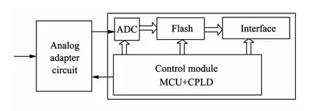
Fig.1 Structural diagram of storage test system
Voltage test and noise test are carried out by different processes for sampling signals.The sampling frequency of each channel is 1 MHz.Sampled signal VIN is divided into two parts:one part goes through the divider to be voltage signal CH1,the other part is filtered to be noise signal CH2.Then both signals go through the multi-selector switch MAX4634 to be stored alternately.
The circuit is triggered by internal signal.After power is on,the system begins to record information before triggered.When the projectile is fired,high impact,overload and high rotation make the fuze battery activated.When the system detects high voltage of fuze battery repeatedly,it starts to store information sequentially.A/D converter samples data with a frequency of 100 Hz;Flash is controlled by MCU to read,write or erase data;CPLD transmits the output data of A/D converter and MCU toflash.
The system principle diagram is shown in Fig.2 .
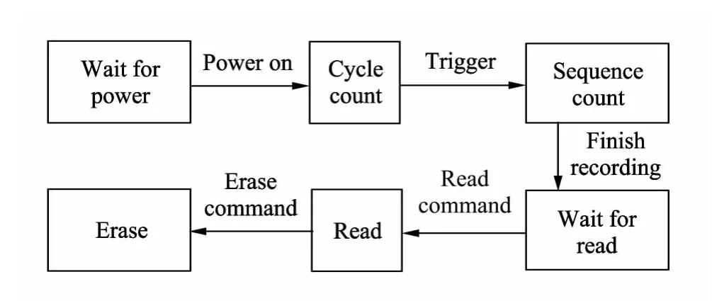
Fig.2 Principle diagram of storage test system
2 Key technologies
2.1 Negative delay technology
In order to observe the changes of voltage and noise at the moment of firing instantly,the signals should be stored before the trigger signal arriving,which is called negative delay.The trigger point is treated as time zero,the data recorded before the trigger point is called negative delay data,and the data after the trigger point is positive delay da-ta[5,6].
The storage space needs to be divided into two parts to avoid negative delay data occupying all memory.The whole Flash memory space includes two parts:one is the negative delay cycle storage space(4 MB),recording data before triggered;the other is continuous memory space(50 MB),recording data after triggered.The changes of triggering signal TR is monitored by CPLD.TR is low in pretriggering period;after triggered,it goes high by a pull-up resistor.After CPLD monitors high level of TR continuously (to prevent false triggering),it sends a triggering signal to MCU,and then the system enters a working condition of circle recording.
The Flash memory space allocation is shown in Fig.3.Point A is the start of 4 MB cycle space,and point C represents the triggering point.The 50 MB memory space begins at point B and ends at point D.After power is on,the entire acquisition module is under working condition,and the data converted by A/D converter is stored in the cycle space.When recording data to point B sequentially,the address pointer jumps back to point A to store new data continuously,recovering the old data.The previous data is overwritten by new data to ensure that Flash keeps 4 MB data for the pre-trigger.Once the moment C the triggering occurs,MCU puts the address information of point C into its internal E2PROM,and the address pointer jumps out of negative delay storage space into continuous storage space,while data storage address changes from point C to point D.Then the data will be stored into the continuous memory space until it reaches point D[7,8].Finally,the circuit stops working and turns into a low-power state.
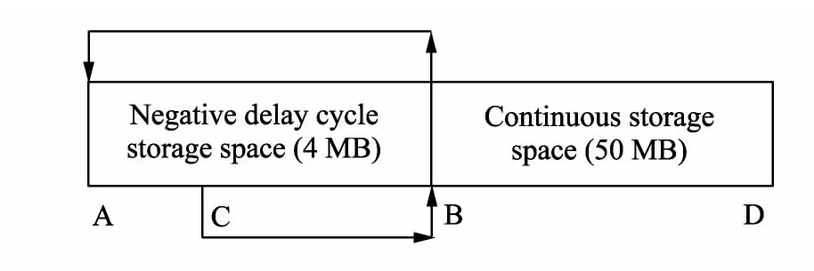
Fig.3 Flash storage space allocation
2.2 Rapid storage technology
Ultimate realization of the storage test is achieved by displaying data entirely and correctly.The low sampling frequency leads tofewer data obtained and increases error when data is restored,so the storage system ought to achieve high-speed sampling.This design uses two pieces of Flash working simultaneously to avoid wasting time of programming in order to achieve high-speed sampling.
Two pieces of Samsung K9F4G08U0B chips are used as Flash.Capacity per chip is 512 MB,reading and programming in pages,and erasing in blocks.The typical time from programming to nonvolatile media of one page(2 KB)is 200μs,up to 700μs;erasing a block(128 KB)takes 1.5 ms[9].But the time that A/D converter outputs data is 1μs,which causes a conflict between programming time and storing time,resulting in loss of data.Therefore,the system uses two pieces of Flash working simultaneously.While it sends control commands to one piece of Flash,the data is sent to another piece of Flash.
A 12-bit data will be output every 10 μs by AD7492.The 12-bit data is turned into 16-bit data by CPLD and divided into high 8-bit and low 8-bit before it is stored into the cache.The data is sent intoflash after it is deposited to 2 KB.It lasts for 1 ms that A/D converter outputs 2 KB data,which is longer than 700μs,ef fectively avoiding the conflict between commands and data.
The capacity of two pieces of Flash can be 108 MB,which meets the test requirements.The system state diagram of writing data toflash A and command toflash B is shown in Fig.4 .
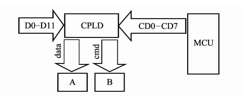
Fig.4 System state diagram when a Flash is written
To indicate Flash states of read,write and erase,0 X01 unit in E2PROM is used as flag showing the system state.The data 0X00 illustrates that Flash is empty.After Flash goes to initialization,the system enters the cycle writing state;if 0XAA is read,the data has already been read;0X55 indicates “not read”.When the system is not read,the system will not be allowed to receive erase interrupt to ensure the validity of data for each sample.After the sampling data has filled up one page,whether this page is the last one for the block will be determined.If it is,the next block will be erased;if not,the next page begins.
3 Negative delay test
The onboard telemetry system has been applied to a practical battery performance test.Under the shock acceleration of approximate 60 000 g,the system works properly.The measured fuze battery voltage and noise curves are shown in Fig.5.It can be seen that the system records the battery information effectively before triggered,and instantaneous voltage changes after triggered.Therefore,the accuracy and reliability can be verified when the onboard telemetry system is in practice.
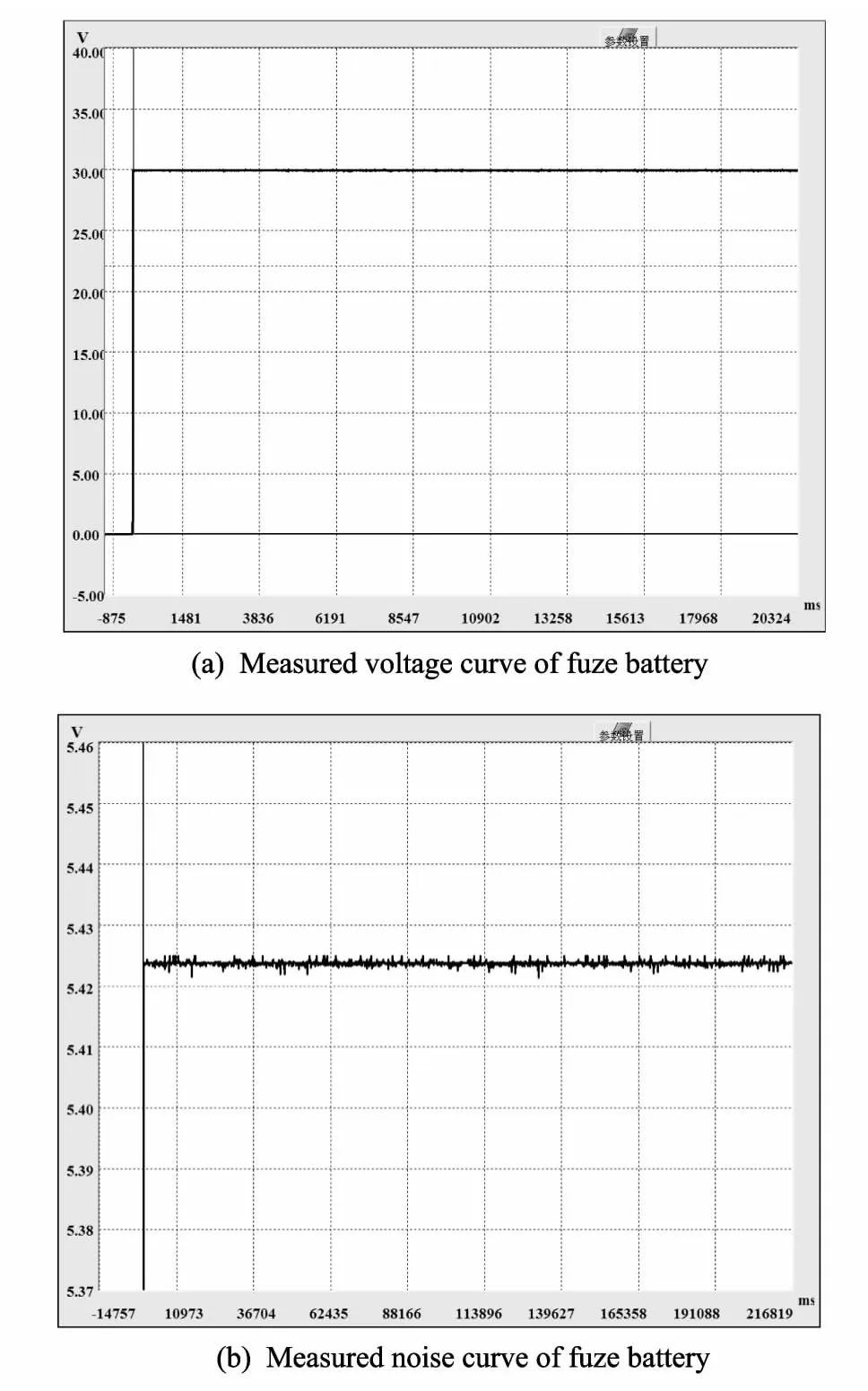
Fig.5 Negative delay test results
4 Conclusion
A negative delay system with rated capacity and cycle storage is designed.It uses MCU and CPLD as control devices and two pieces of Flash as mass data storage to record the output of fuze battery under any condition.CPLD as high-frequency sampling signal producer and MCU as the controller of Flash work alternately.Test results show that the designed system not only makes the sampling frequency up to 1MHz but also clearly shows the activation time,duration and transient change of noise.Moreover,it can show the information of fuze battery before and after activation,ensuring the integrity and analyzability of the measured signal.
[1]WANG Zhen.Effect of chemical battery on the design of radiofuze.Journal of Gansu Sciences,2003,15(2):107-108.
[2]JIANG Zhi-bao,ZHENG Bo,ZHANG Feng-ying.Electrical fuses based on virtual instrument test battery performance.Journal of Sichuan Ordnance,2008,29(6):45-50.
[3]LU Yu-qi,WANG Xiao-feng,RUI You-ting,et al.Study on the dynamics of the fuze mechanism.Journal of Nanjing University of Science and Technology,2000,(6):228-231.
[4]QIAN Hai-ying,GAO Ru-ming,WANG Hong-xuan.Study on simulation of double environmental forces of liquid reserve battery for fuses.Structure and Environment Engineering,2013,40(1):58-63.
[5]JIN Hong,ZU Jing.A storage measurement system for fuze batteries based on microcontroller.Journal of Detec-tion and Control,2009,31(1):70-73.
[6]ZHANG Wen-dong.Storage test system design theory and its missile tests in the realization of dyoamic data.Ph D thesis.Beijing Institute of Technology,1995.
[7]YAN Xin.The design of re-issued data memory circuit based on telemetry system.Master Thesis.North University of China,2012.
[8]MA Tie-hua.Storing test technology development and application and research of special sensor technology.Postdoctoral research report.Beijing Institute of technology,1999.
[9]Samsung Semiconductor.K9F1G08R0A-128 M×8 bit/256 M×8 bit NAND Flash memory product specification.Samsun Co.,2005.
