Influence of In-situ SiNxInterlayer on Strain Relief and Optical Character of GaN Epilayer Grown on 6H-SiC
SONG Shi-wei,LIANG Hong-wei,2* ,SHEN Ren-sheng,
LIU Yang1,ZHANG Ke-xiong1,XIA Xiao-chuan1,DU Guo-tong1,3
(1.School of Physics and Optoelectronic Technology,Dalian University of Technology,Dalian 116024,China;2.State Key Laboratory of Functional Materials for Informatics,Shanghai Institute of Microsystem and Information Technology,Chinese Academy of Sciences,Shanghai 200050,China;3.College of Electronic Science and Engineering,Jilin University,Changchun 130012,China)
1 Introduction
Recent years,GaN has attracted much attention for the application of light emitting diode(LED),solar cells,UV detectors,and so on[1-3].But growth of GaN itself suffers a series of problems.Due to lack of sui
Table native substrates,GaN generally has been heteroepitaxied on foreign substrates such as SiC,sapphire,introducing a high density of threading dislocations(TDs)in the range of 109~1010cm-2and experiencing a considerable biaxial strain[4].
Compared to sapphire,SiC substrate is admired as a more suitable substrate for the advantage of lattice mismatch(3.4%),high electrical and thermal conductivity.Therefore,a vertical LED structure can be realized.To further improve the lifetime of the LED,some methods including majorization the crystalline quality of GaN epilayer have been proposed,such as epitaxial lateral overgrown(ELOG),AlN buffer layer is introduced[5-6].ELOG can reduce the TDs to 105cm-2in the wing region,leaving 109cm-2TDs in the window region[7],and needs a larger thickness until complete coalescence and to cause cracking.Also,AlN is insulating,hard to be doped,which is disadvantageous to realize a vertical LED.The in situ SiNxnano-mask is thought to be an effective method to decrease dislocation density by two or three orders of magnitude[8-9].Generally,most attention was paid to the improvement of crystalline quality,the strain relief was ignored.In this letter,we report the strain relief of the 5 μm GaN grown on(0001)6H-SiC by in-situ SiNxnano-mask,and the mechanism is systematically analyzed also.
2 Experiments
The GaN epilayers with thickness about 5 μm were grown on Si-terminate n-type(0001)6H-SiC using low-pressure metal organic chemical vapor deposition(LP-MOCVD)in a Thomas Swan 3×2 close-coupled showerhead reactor.The substrates were commercial wafers with on-axis direction.Trimethyl-gallium(TMGa)and trimethyl-aluminum(TMAl)were used as precursors of Ga and Al,ammonia(NH3)was used as the nitride source,and the n-type dopant was silane(SiH4).Reflectivity data and the wafer temperature were recorded in situ using a LayTec EpiTT monitor with a 633 nm laser.The samples were first heated up to 1 100℃for hydrogen(H2)baking to remove the native oxide,followed by an AlGaN nucleation layer(NL):TMGa and TMAl flow were on 21.99 μmol/min and 4.68 μmol/min,respectively,while NH3flow was 0.134 mol/min.Then,a composition graded AlGaN was deposited,the TMAl flow decreased to 0 uniformly,while the TMGa increased to 175.9 μmol/min simultaneously.After the deposition of composition graded AlGaN,a 1 μm GaN template was prepared at the same temperature and the mole ratio of nN/nGawas 1 269.Then,a SiNxnano-mask was induced by the same temperature,reactor press and NH3flow,while TMGa was closed and SiH4flow increased to three times in 10 s.Samples A,B,C were denoted by the SiNxdepositon time of 0,2,4 min.After SiNxinterlayer growth,a 4 μm GaN epilayer was sequentially grown with the same condition as the former deposition process of GaN.All samples in this paper are n-doped with a concentration of 3×1018cm-3.
Renishaw in Via Raman microscope was used to obtain Raman spectra.Olympus BX51M optical microscope was taken to examine the surface crack line density.Photoluminescence(PL)was carried out by a HR-300 CCD spectrometer with He-Cd 325 nm laser.The crystalline quality of the GaN epilayers were estimated by high-resolution X-ray diffraction(XRD)using Bede D1 XRD equipment.
3 Results and Discussion
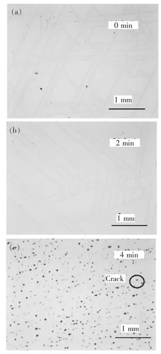
Fig.1 exhibited the optical microscopic images of three samples.Two kinds of defects can be seen:dark pits and cracks.The dark pits from non-coalesced surface regions indicate that a more growth time is needed while the cracks are due to a layer thickness larger than the critical value.The strain induced by lattice mismatch between GaN/SiC is compressive as evident from the different in-plane lattice constants(aGaN=0.318 8 nm,aSiC=0.308 1 nm)[10].Thus,the difference of thermal expansion coefficients between GaN and SiC is a source of significant biaxial tensile strain which caused crack in the GaN epilayer during cooling(αGaN=5.6 ×10⁻⁶/K,αSiC=4.2 ×10-6/K)[11].Another source could be resulted from Si doping[12].With an insertion of 2 min nano-SiNxinterlayer,the crack line density was slightly reduced from 2.82 mm-1to 1.93 mm-1,and to 0.29 mm-1by a 4 min nano-SiNxinterlayer.It seems that the induced nano-SiNxinterlayer can decrease crack line density as a result of strain relaxation.

Fig.1 Optical microscopic images of(a)sample A without SiNx,(b)sample B with 2 min nano-SiNxinterlayer,(c)sample C with 4 min nano-SiNxinterlayer.The scale bars in all images are 1 mm.
Prior to this conclusion,the Raman measurement is performed that the E2high mode in the Raman spectra has been proven to shift by biaxial stress only[13].A tensile stress will result in a photon frequency red-shift while a compress stress must be responsible for a photon frequency blue-shift.As seen from table 1,the E2phonon lines of GaN layers in this study all subjected to a low-frequency shift,which is indicative of the existence of a biaxial tensile strain in GaN layers.In order to understand the variation of strain state in different samples,the strain can be valued by the formula of photon frequency shift of E2phonon mode in terms of the biaxial stress

Where Δω is the photon frequency shift(cm-1)and ω is the photon frequency shift of 568.0 cm-1for a strain-free bulk GaN[13],while εxxis the in-plane stress,aλand bλare the deformation potential constants,valued -850 cm-1and -920 cm-1for calculation[14],and q= -2C13/C33= - 0.54[15].The observed 2.9,2.5,1.9 cm-1photon frequency shift according to the phonon energy of E2mode for a strain-free bulk GaN gives a biaxial tensile strain of 2.41 × 10-3,2.08 × 10-3,1.58 × 10-3for three samples,respectively.

Table 1 Displays the photon energy E10Kof(D0X)PL at 10 K,the room temperature Raman E2mode and the FWHM of(002)and(102)diffraction peaks of GaN epilayers with different nano-SiNxtime(0~4 min)
It is reported that tensile strain could be induced by the threading dislocation(TD)[16].Therefore,we support our assignment of the strain relief to the TDs by performing XRD measurement.Both symmetric(002)and asymmetric(102)XRD rocking curves are performed,the full width at half maximum(FWHM)of(002)diffraction is correlated with the density of screw dislocations,whileasymmetric(102)is sensitive to the pure edge and mixed dislocations[17].The TD density can be calculated by the following equation[18]:

Where ρsis the screw dislocation density,ρeis the edge dislocation density,β(002)and β(102)are the full width at half maximum(FWHM)of(002)and(102)diffraction,while bsand bEare Burger vector sizes of the screw(c=0.518 5 nm)and edge(a=0.318 8 nm)components.According to the FWHM of XRD given in table 1,the screw dislocation densities are calculated as 7.8 ×107cm-2,6.6 ×107cm-2,5.1 ×107cm-2for three samples,and the edge dislocation densities are 5.3 ×108cm-2,4.7 × 108cm-2,2.7 × 108cm-2.Obviously,the in situ SiNxinterlayer impedes dislocation effectively,which can be explained by two termination:One is that the nano-SiNxmask is preferentially formed at the TD cores because of the presence of N-dangling bonds for Si-N formation[19];another possible mechanism of TD termination is 3D growth mode induced by SiNxinterlayer as our previous report[20],lots of TDs bend to the facetted islands.Some TDs with an opposite Burgers vector could be annihilated when forming half-loops after reacting with each other at the interface,and some non-annihilated TDs would bend a certain angle,if the subsequent GaN epilayer thick enough,TDs would not propagate to the surface.
Fig.2 shows the variation of in-plane stress and TD density as a function of SiNxinterlayer deposition time.It can be seen that as the TD density decreases,the in-plane stress relieves.After growth,the GaN epilayer is cooled from high temperature,the thermal mismatch tensile strain is induced and there will be some rearrangement of TD in response to this change[21].The TD would climb in the epilayer and relieve the residual stress.Therefore,the decreasing in TDs would increase the residual stress,which compensates the tensile stress accompanied during the cooling down to room temperature.

Fig.2 Variation of in-plane stress and TD density as a function of SiNxinterlayer deposition time
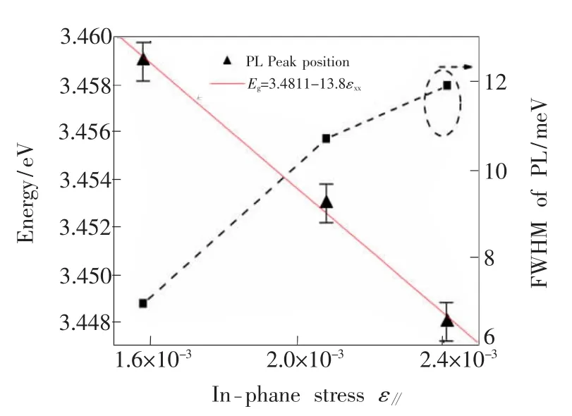
It is well known that the residual stress can affect the energy band gap and a tensile stress will result in a decrease of energy band gap while a compress stress causes an increase of band gap.By least-square fitting of the data from the peak position of low temperature PL spectra,the band gap of GaN at 10 K can be expressed in terms of biaxial stress according to:

Fig.3 exhibits the relationship between FWHMs of emitting peaks and the in-plane stress.As the inplane stress is relived,the FWHM decreases also,which indicates that the strain relief by induced SiNxinterlayer considerably improved the optical properties of GaN.

Fig.3 The photon energy and FWHMs of emitting peak vs.the in-plane stress.The solid line represents a linear fitting result to the experimental data.
4 Conclusion
The in situ porous SiNxinterlayer during the growth of GaN epitaxial layers is served to relieve strain.SiNxinterlayer is helpful to mitigate the crack problem commonly experienced in GaN grown on SiC substrate.Indeed,the biaxial tensile stress quantitatively analyzed by Raman and gives a tensile stress reduction from-2.41 ×10⁻³to -1.58 ×10⁻³by SiNxinterlayer induced,which is responsible to dislocations reduction.A linear relationship of the luminescent band gap of GaN with the residual stress at low temperature is observed,and a linear coefficient of 13.8 eV is derived.
[1]Nakamura S.The roles of structural imperfections in InGaN-based blue light-emitting diodes and laser diodes[J].Science,1998,281(5379):956-961.
[2]Jani O,Ferguson I,Honsberg C,et al.Design and characterization of GaN/InGaN solar cells[J].Appl.Phys.Lett.,2007,91(13):132117-1-3.
[3]Martens M,Schlegel J,Vogt P,et al.High gain ultraviolet photodetectors based on AlGaN/GaN heterostructures for optical switching[J].Appl.Phys.Lett.,2011,98(21):211114-1-3.
[4]Ng H M,Doppalapudi D,Moustakas T D,et al.The role of dislocation scattering in n-type GaN films[J].Appl.Phys.Lett.,1998,73(6):821-824.
[5]Gmeinwieser N,Engl K,Gottfriedsen P,et al.Correlation of strain,wing tilt,dislocation density,and photoluminescence in epitaxial lateral overgrown GaN on SiC substrates[J].J.Appl.Phys.,2004,96(7):3666-3672.
[6]Ponce F A,Krusor B S,Major J S,et al.Microstructure of GaN epitaxy on SiC using AlN buffer layers[J].Appl.Phys.Lett.,1995,67(3):410-412.
[7]Fujito K,Kiyomi K,Mochizuki T,et al.High-quality nonpolar m-plane GaN substrates grown by HVPE [J].Phys.Status Solidi(a),2008,205(5):1056-1059.
[8]Kappers M J,Datta R,Oliver R A,et al.Threading dislocation reduction in(0001)GaN thin films using SiNxinterlayers[J].J.Crystal Growth,2007,300(1):70-74.
[9]Fareed R S Q,Yang J W,Zhang J,et al.Vertically faceted lateral overgrowth of GaN on SiC with conducting buffer layers using pulsed metalorganic chemical vapor deposition [J].Appl.Phys.Lett.,2000,77(15):2343-2346.
[10]Romano L T,VandeWalle C G,Ager J W,et al.Effect of Si doping on strain,cracking,and microstructure in GaN thin films grown by metalorganic chemical vapor deposition [J].J.Appl.Phys.,2000,87(11):7745-7752.
[11]Porowski S.Bulk and homoepitaxial GaN-growth and characterization[J].J.Cryst.Growth,1998,189-190:153-158.
[12]Ponce F A,Krusor B S,Major J S,et al.Microstructure of GaN epitaxy on SiC using AlN buffer layers[J].Appl.Phys.Lett.,1995,67(3):410-412.
[13]Perlin P,Jauberthie C C,Itie J P,et al.Raman scattering and X-ray-absorption spectroscopy in gallium nitride under high pressure[J].Phys.Rev.B,1992,45(1):83-89.
[14]Davydov V Y,Averkiev N S,Goncharuk I N,et al.Raman and photoluminescence studies of biaxial strain in GaN epitaxial layers grown on 6H-SiC [J].J.Appl.Phys.,1997,82(10):5097-5102.
[15]Polian A,Grimsdich M,Grzegory I.Elastic constants of gallium nitride[J].J.Appl.Phys.,1996,79(6):3343-3344.
[16]Taniyasu Y,Kasu M,Makimoto T.Threading dislocations in heteroepitaxial AlN layer grown by MOVPE on SiC(0001)substrate[J].J.Cryst.Growth,2007,298:310-315.
[17]Romanov A E,Speck J S.Stress relaxation in mismatched layers due to threading dislocation inclination[J].Appl.Phys.Lett.,2003,83(13):2569-2571.
[18]Takeuchi M,Shimizu H,Kajitani R,et al.Al-and N-polar AlN layers grown on c-plane sapphire substrates by modified flow-modulation MOCVD[J].J.Cryst.Growth,2007,305(2):360-365.
[19]Tanaka S,Takeuchi M,Aoyagi Y.Anti-surfactant in III-nitride epitaxy-quantum dot formation and dislocation termination[J].Jpn.J.Appl.Phys.,2000,39:L831-L834.
[20]Yang D C,Liang H W,Song S W,et al.Improvement of the quality of a GaN epilayer by employing a SiNxinterlayer[J].Chin.Phys.Lett.,2012,29(10):088102-1-4.
[21]Sun X Y,Bommena R,Burckel D,et al.Defect reduction mechanisms in the nanoheteroepitaxy of GaN on SiC[J].J.Appl.Phys.,2004,95(3):1450-1454.
