A window-based accelerating algorithm for SDA integration
YU Bao-chu, YU Qing-jun, YU Tie-jun, TANG Zhen-an
(1.State Key Laboratory of Structural Analysis for Industrial Equipment,Dalian University of Technology,Dalian 116024,China;2.School of Civil Engineering,Dalian Ocean University,Dalian 116023,China;3.School of Electronic Science and Technology,Dalian University of Technology,Dalian 116024,China)
0 Introduction
The design of high performance IC systems requires accurate high frequency analysis of interconnects.Frequency dependence analysis of interconnect or transmission line,especially the on-chip interconnect with substrate loss plays an important role in the chip signal integrity.In the silicon-based chip design,due to the loss substrate′s collecting and redistributing of the digital switching noise,mixed signal chip design faces serious challenge.Spectral domain analysis or approach(SDA),which is a standard fullwave method[1],is proposed here to do the onchip interconnect analysis.However,the traditional SDA is very time-consuming due to the infinity integration of the system matrix′s entries in the spectral domain(SD).To overcome this difficulty,new numerical technique is needed to speed up SDA.Window function accelerated techniques are widely used in the signal processing and other applications.In fact,the concept of using window accelerated technique to speed up the integration itself is not a new one,but how to compose the appropriate window function,how to derive the acceleration algorithm is a very creative process in the SDA.In Lits.[2,3],a 2-dimensional low-pass-filter window(LPFW)is successfully used to speed up the layered Green′s function calculation.Here,this paper will introduce another new 1-dimensional LPFW and derive its spectral closed-form formulation.Based on this new window,a novel accelerating algorithm will be derived to speed up the traditional SDA integration calculation.The approach used here is also useful for other applications,e.g.,how to determine the earthquake destructive capability for its first few arrived shocking waves during the rupture.
1 SDA and its problems
1.1 SDA introduction
Fig.1 shows the considering problem which is a multi-layered interconnects′cross section.Interconnect width is noted as″W″,while its thickness is noted as″t″.Each dielectric layer is defined as homogenous and is specified byεi,μi,σi.For a real silicon on-chip interconnect,it usually consists of a ground plane with a few hundred micron-meters thick loss substrate layer and then a very thin oxide layer which separates the first metal layer and the loss substrate.Here assuming the electromagnetic(EM)wave propagates in thexdirection and a factor ejωt-jkx xis suppressed in the later formula derivation.Complex propagation constant(k x=β-jα)is the solved object which represents the EM wave speed and also its attenuation information.With the Green′s function′s[3,4]taking care of the substrate,layered dielectric and ground plane′s effects,the integration equation can be generated only on the metal interconnect strip surface.The electric field on the metal strip surface can be expressed in terms of Green′s function as
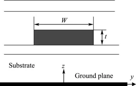
Fig.1 Cross section of the multi-layered interconnect

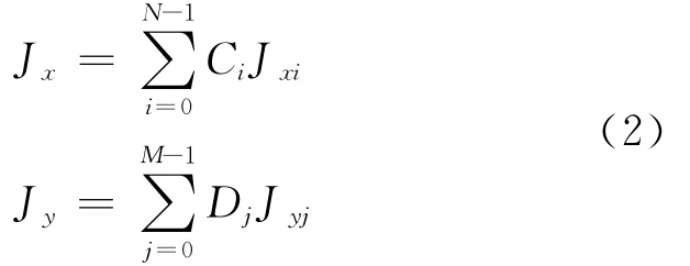
WhereGis the multi-layer electric field Dyadic Green′s function;Jis the current distribution on the metal strip,which can be expressed in terms of the basis functions ofJ xi,J yj,they are
Metal strip with thickness oftcan be considered as a complex resistive thin film with the effective surface resistanceZs.On the strip surface,the boundary condition is

Following the SDA standard procedure in spectral domain[1,5],multiplying the each current basic functionJxi,Jyjat both sides of Eq.(3);doing the integration in the corresponding support of the basic function ofJ xi,J yj,and transferring the integration into spectral domain,then system equation is arrived as follows:

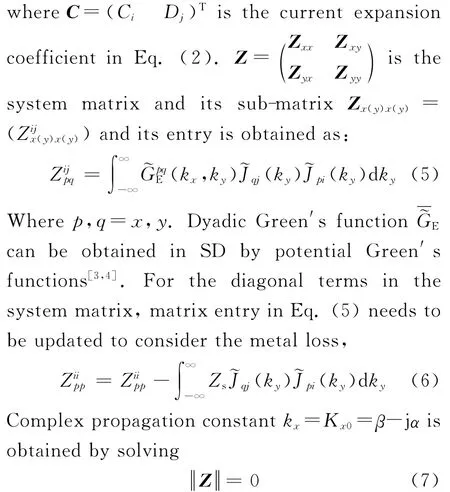
Usually Eq.(7)can be solved with Newton-Raphson iteration.Current distributionC=(CiDj)Ton the strip can be determined in a least square sense from Eq.(4)afterK x0is obtained.
1.2 SDA problems
SDA is a full wave solution in which almost all the EM issues in interconnect are considered and therefore,it is a very accurate approach.Also as the operation is done in the spectral domain,the complicate Green′s function calculation in the spatial domain is avoided.However,SDA faces a serious challenge.It is extremely time-consuming to calculate the infinity integration shown in Eqs.(5),(6).This can be explained as follows.Usually,basis functions in Eq.(2)are given as:
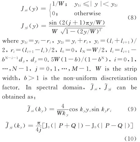
Where J0is the zero order Bessel function,P=0.5Wk y,Q=(j+1)π.Eqs.(9),(10)show thatoscillate fastly and decay slowly.Alsousually varies fastly and decays slowly especially at higher frequency with bigger number of layers.Asandare all slowly decaying and fastly oscillating functions,this leads to the longer integration interval with densely sampling points in the integration of Eq.(5)and Eq.(6)which makes the calculation very expensive.That is the main issue SDA faces.
2 Window function and its fast algorithm
2.1 Motivation
To speed up Eqs.(5),(6),one can shorten the integral interval or reduce the sampling points′number.This paper is focusing on how to shorten the integral interval.A new window function named″w″is designed to do so. If″w″decays very fast,and if″w″multiples the integral kernel in Eqs.(5),(6),then the new integral kernel should decay fast because the″w″decays fast.To reach this goal the″w″must decay very fast in the spectral domain,and in the mathematical point of view,″w″must have a compact supporting and must be very smooth in the spatial domain,so its spectral domain(SD)component is a low-pass-filter window(LPFW)and decays fast.LPFW indicates that the low spectral components are filtered in the integration while the high spectral components are phased out.
Applying theorem
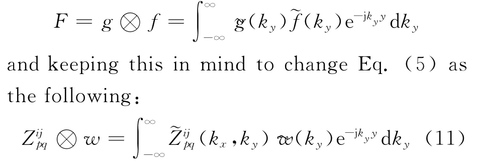
Ifw槇decays very fast,then the integral interval in the right side of Eq.(11)will be shortened dramatically.However,the left side of Eq.(11)is notas stated in Eq.(5),but a convolution ofwith the window of″w″.To recover the value offrom the convolution,Taylor series are used in the left side of Eq.(11)to expandat some fixed points as follows:

The second term in the integral of Eq.(12)can be chosen symmetrically and is 0,so one can finally obtain the following:

Combining Eq.(11)and Eq.(13)to get the fast algorithm:

WhereM0=∫w(τ)dτis called the first order moment of″w″,which is the integrated area under the curve of″w″.
2.2 Window function
How to construct the appropriate″w″is the key point to make sure the fast algorithm′s success.According to the required properties of″w″,design it as:

Wheremis the order of″w″,ais the compact support of″w″.Its SD component,槇w,can be derived as:

whered=k yaandw′s first moment is derived as:

2.3 Fast algorithm
The fast algorithm Eq.(14)requires珟Zijpqbut there is onlyZijpqin Eq.(5),so hereZijxxis used as an example to show how to derive the fast algorithm.In Eq.(5),after doing some derivation one can get
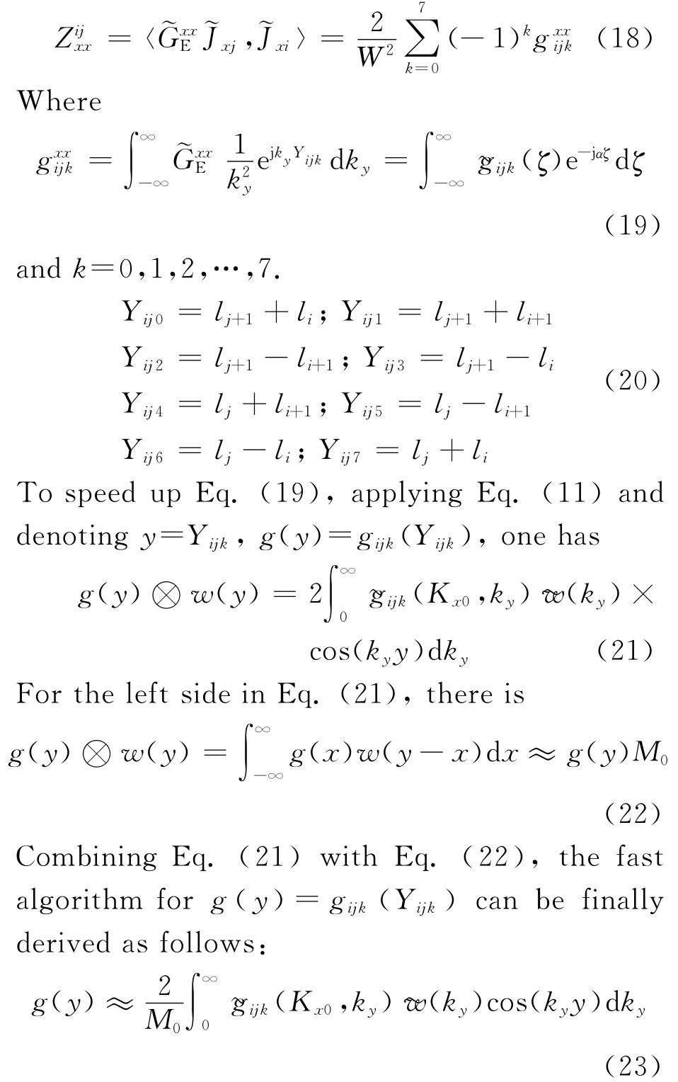
Similar to,other entries in Eqs.(5)-(6)also can be accelerated by the window-based algorithm.
3 Numerical experiments
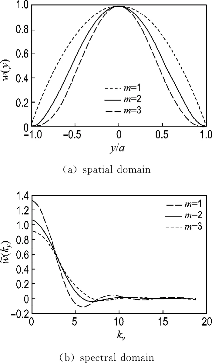
Fig.2 Window functions
Check window″w″itself first.Fig.2 shows the window function both in the spatial and spectral domain.One can see that in the spatial domain it is very smooth.The bigger themin Eq.(15)is,the smoother the window function in the spatial domain is.In this sense,namingmas the order of the window function,cases wherem>1 are referred to the higher order window functions.Also from Fig.2 one can see that if the order is high,the window′s spectral component槇w(k y)in Eq.(16)will be more complicated and decay faster.Decaying fast is the preferred feature,but too complicated槇w(k y)is not wanted because it will slow down the calculating speed in Eq.(14).So in this study,manymvalues are tried,but onlym=1,2,3 are used in the final calculation.The distribution of the window function in both domains in Fig.2 shows that″w″is well constructed with a very deep descent feature in the higher spectral domain.The bigger the ordermis,the smoother″w″is and the faster槇wdecays.
Shown in Eq.(23),槇w′s decaying determines the fast algorithm′s gain respective to the traditional SDA.When focusing on the speed gain by using window-based acceleration,define the gain ratio as

whereLdandLware the integration interval ofk yused in Eq.(19)and Eq.(23)respectively.Tab.1 shows the speedup behaviors when″w″is used to accelerate the integrations.From Tab.1 and other experiments,it is found that 10-100 times of speedup ratio can be achieved by using this window function of″w″with accuracy loss within 1%.
Tab.1 Speedup comparison(Speedup :Case 2 in Fig.3 is used here with f=1 GHz,K x0=107.6-j28.8,N=4,M=5,b=2.0 in Eq.(8).Widows′order m=1,for window w1,a=0.3d y;for w2,a=0.15d y,d y is defined in Eq.(8))
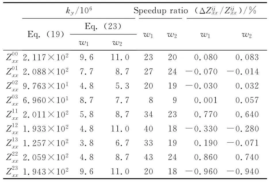
Tab.1 Speedup comparison(Speedup :Case 2 in Fig.3 is used here with f=1 GHz,K x0=107.6-j28.8,N=4,M=5,b=2.0 in Eq.(8).Widows′order m=1,for window w1,a=0.3d y;for w2,a=0.15d y,d y is defined in Eq.(8))
ky/106 Speedup ratio(ΔZijxx/Zijxx)/% Eq.(19) Eq.(23)w1w2 w1 w2w1w2 Z 00xx 2.117×102 9.6 11.0 23 20 0.080 0.083 Z 01xx 2.088×102 7.7 8.7 27 24-0.070-0.014 Z 02xx 9.763×101 4.8 5.3 20 19-0.030 0.032 Z 03xx 6.960×101 8.7 7.7 8 9 0.001 0.057 Z 11xx 2.011×102 5.8 8.7 34 23 0.770 0.640 Z 12xx 1.933×102 4.8 11.0 40 18-0.330-0.280 Z 13xx 1.257×102 3.8 6.7 33 19 0.190-0.071 Z 22xx 2.059×102 4.8 8.7 43 24 0.860 0.740 Z 23xx 1.943×102 9.6 11.0 20 18-0.960-0.940
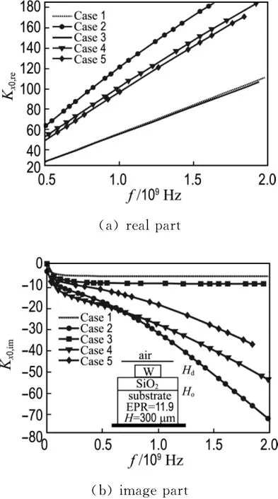
Fig.3 Propagation constant K x0 comparison of CMOS on-chip interconnect
The study of complex propagation constantK x0is also shown here after the new fast SDA algorithm is developed.ForK x0is the most important parameter of a transmission line or an on-chip interconnect.The fast algorithm is first validated by comparing it to the closed-formulas of microstrip special case.Then,for the multilayer cases,the new fast SDA algorithm results are compared to the results obtained by IE3D[6],also compared to the measurement results[7].All the comparison shows the new fast algorithm works very well.After validation,the on-chip interconnect studying with the new fast SDA algorithm focuses on CMOS interconnect lines.Fig.3 shows 5 different cases′K x0studying.Case 1 has no substrate loss,dielectric and oxide layer thicknesses areHd=47μm,Ho=1.5μm respectively.Interconnect is made of aluminum with cross section as 13μm×2μm;Compared to Case 1,the only change in Case 2 is that it has substrate loss,substrate conductivityσ=10 S/m;Case 3 is the same as Case 1,but the interconnect widthWis cut by half in whichW=6.5μm;Case 4 is the same as Case 3 but with substrate loss;case 5 is the same as Case 4,but the oxide layer thickness is doubled asHo=3 μm.Fig.3 sheds very interesting lights on the loss substrate′s impacting on the signal propagation:Substrate loss is much bigger than the metal loss itself in this case,but if the interconnect is far away from substrate,the substrate loss will be reduced dramatically.On the other hand,substrate loss also has impact on the signal phase velocity,heavier substrate loss forms slower wave propagation on interconnect confirms the expectations.
4 Conclusion
A novel low-pass-filter window function(LPFW)is constructed to shorten the infinity integral interval in the traditional SDA calculation of on-chip interconnect or MMIC transmission line.Without sacrificing the accuracy,the speedup ratio can be up to 100 times in most numerical experiment cases.The proposed window-based acceleration method in the integration can be widely used due to its general outline in principle.Finally,from the engineering point of view,as槇w(k y)closedformulation is explicitly known,so when applying Eq.(23)to the numerical integration,user can control the integration accuracy by adjusting the window′s compact support easily and therefore it is good for robust coding development.
[1]LEE H Y,ITOH T.Phenomenological loss equivalent method for planar quasi-TEM transmission lines with a thin normal conductor or superconductor[J].IEEE Transactions on Microwave Theory and Techniques,1989,37(12):1904-1909
[2]YU T,CAI W.High-order window functions and fast algorithms for calculating Dyadic Green′s function functions in the multilayered media[J].Radio Science,2001,36(4):559-569
[3]YU T,CAI W.FIFA-fast interpolation and filtering algorithm for calculating Dyadic Green′s function in the EM scattering of multi-layered structures[J].Communication in Computational Physics,2006,1(2):229-260
[4]MICHALSKI K,ZHENG D.Electromagnetic scattering and radiation by surfaces of arbitrary shape in layered media.I.Theory[J].IEEE Transactions on Antennas and Propagation,1990,38(3):335-344
[5]YU Tie-jun,ZHANG Xue-xia,GUO Bao-xin,etal.The current distribution of high-Tc superconducting microstrip lines[J].IEEE MTT-S International Microwave Symposium Digest,1996,3:1667-1670
[6]Vikingboy.Zeland IE3D:Mo M-Based EM Simulator 14.1[S/OL].[2008-10-21]http://www.mentor.com/electromagnetic-simulation
[7]TIEMEIJER L F,PIJPER R.On the accuracy of the parameters extracted from parameter measurements taken on differential IC transmission line[J].IEEE Transactions on Microwave Theory and Techniques,2009,57(6):1581-1588
