超声搅拌化学浴沉积法制备大颗粒和致密的CdS薄膜
史成武 陈 柱 史高杨 孙人杰
(1合肥工业大学化学工程学院,合肥230009;2中国科学院新型薄膜太阳电池重点实验室,合肥230031)
超声搅拌化学浴沉积法制备大颗粒和致密的CdS薄膜
史成武1,2,*陈 柱1,2史高杨1,2孙人杰1
(1合肥工业大学化学工程学院,合肥230009;2中国科学院新型薄膜太阳电池重点实验室,合肥230031)
采用超声搅拌化学浴法(UCBD)在SnO2:F透明导电玻璃衬底上制备了CdS薄膜.研究了退火和CdCl2处理对UCBD-CdS薄膜的表面形貌、晶体结构和直接带隙的影响,比较了沉积时间对UCBD-CdS薄膜中CdS聚集体颗粒大小和堆积致密性的影响.结果表明,CdCl2处理可使CdS聚集体中的小颗粒重新熔合在一起,但CdS聚集体的大小并没有改变.在UCBD-CdS薄膜的沉积过程中,CdS薄膜的横向和纵向生长速率之比会随着沉积时间的不同而改变,且沉积时间是获得大颗粒的CdS聚集体和致密的UCBD-CdS薄膜的重要影响因素.当沉积时间为40 min时,获得的UCBD-CdS薄膜较致密,CdS聚集体的大小为180 nm,膜厚为80.8 nm,适合作为薄膜太阳电池的窗口层.
CdS薄膜;超声搅拌;化学浴沉积;沉积时间;退火;CdCl2处理
1 Introduction
CdS thin films were widely used as a window layer in the thin film solar cells based on CdTe,1,2CuInGaSe2,3,4and Cu2Zn-SnS4.5The photovoltaic efficiencies of these thin film solar cells were associated with the characteristics of CdS thin films. The CdS thin films can be prepared using various procedures such as thermal evaporation,6sputtering,7spray pyrolysis,8electrodeposition,9screen printing,10physical vapor deposition,11close-spaced sublimation,12,13and chemical bath deposition.14-16Among these techniques,chemical bath deposition method has attracted much attention since it is confirmed as a simple and promissing technique to obtain quality films.To obtain the optimal CdS thin films by chemical bath deposition,the deposition conditions,such as bath solution composition,17-19pH,20deposition temperature,21deposition time,22and CdCl2-treatment procedure,23were investigated.It was well-known that increase of deposition time can increase the thickness of CdS thin films. However,the influence of deposition time on the grain size and stack denseness in the CdS thin films using ultrasonic agitation chemical bath deposition was not reported.And the effect of annealing and CdCl2-treatment procedure on the surface morphology,crystal structure,and direct band gap of CdS thin films using ultrasonic agitation chemical bath deposition was not compared systematically.
In this paper,CdS thin films were deposited on F-doped SnO2transparent conductive glass by ultrasonic agitation chemical bath deposition(UCBD).The influence of deposition time on the grain size and stack denseness in the UCBD-CdS thin films was compared.The surface morphology,crystal structure,and direct band gap of three UCBD-CdS thin films,asgrown,annealing,and CdCl2-treatment,were investigated by scanning electron microscope(SEM),X-ray diffraction(XRD), and UV-Vis spectra.
2 Experimental
2.1 Chemicals and measurement
All chemicals were commercially available and used without further purification.The purity of CdCl2·2.5H2O reagent was 99.999%.The UV-Vis spectra were recorded with a double beam UV-Vis spectrophotometer(TU-1901,China)at a resolution of 0.5 nm.The surface morphology of the UCBD-CdS thin films was observed by a scanning electron microscope (SEM,Sirion 200,FEI,USA).XRD pattern was measured using Cu Kαradiation,40 kV and 30 mA(Philips X´:Pert Pro,Philips,Netherlands).The thicknesses of the UCBD-CdS thin films were determined by the cross-sectional SEM images.
2.2 Chemical bath deposition and CdCl2-treatment of UCBD-CdS thin films
F-doped SnO2transparent conductive glass(FTO)was ultrasonically cleaned by detergent solution for 10 min and later rinsed with deionized water for three times.The aqueous solution composition of UCBD was cadmium acetate(AR,0.01 mol·L-1),ammonium acetate(AR,0.20 mol·L-1)and thiourea (AR,0.05 mol·L-1),and ammonium hydroxide(AR)was added to adjust 9-10 of pH.The deposition was carried out at 80°C for 20,40,60,and 90 min with ultrasonic agitation in ultrasonic cleaning instrument.Then the UCBD-CdS thin films were washed in deionized water and dried in an oven at the temperature of 60°C.The UCBD-CdS thin films for 90 min of deposition time were distributzed into three portions:some UCBDCdS thin films(referred to hereafter as CdCl2-treatment)were immersed into a saturated solution of CdCl2in methanol for 3 min.After drying,the UCBD-CdS thin films were annealed in N2at 450°C for 50 min in a tube furnace,and dipped in hot deioniized water for 5 min.Subsequently they were washed thoroughly in deionized water and dried in a 60°C oven.Some UCBD-CdS thin films(referred to hereafter as annealing)were directly annealed in N2at 450°C for 50 min.The other UCBDCdS thin films(referred to hereafter as as-grown)were used for comparison.The UCBD-CdS thin films deposited for 90 min were used to investigate the surface morphology,crystal structure,and direct band gap.Moreover,the grain size,stack denseness,and thickness of the UCBD-CdS thin films for 20, 40,and 60 min were compared.
3 Results and discussion
3.1 Surface morphology of as-grown,annealing and CdCl2-treatment UCBD-CdS thin films deposited for 90 min
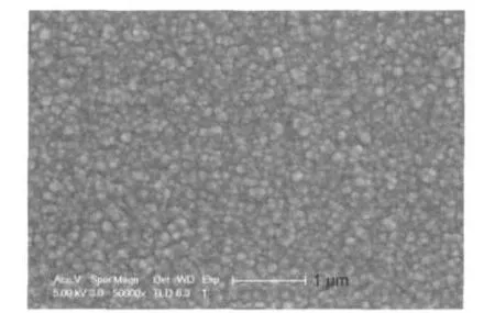
Fig.1 shows the surface morphology of the as-grown UCBDCdS thin film for 90 min of deposition time.
From Fig.1,the UCBD-CdS thin film is homogeneous,freecrack,and smooth.Also,the adsorbed colloidal particles and white boulders,which usually appeared in CdS thin films using chemical bath deposition without ultrasonic agitation,were not observed.The result was in accordance with the literature.24
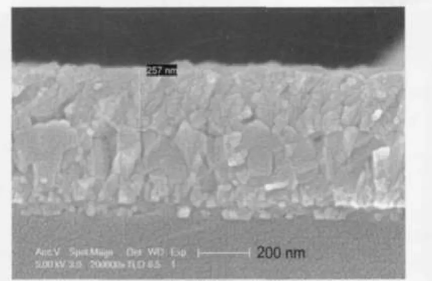
Fig.2 shows the cross-section micrograph of the as-grown UCBD-CdS thin film for 90 min of deposition time.The thickness of the as-grown UCBD-CdS thin film is about 257 nm.

Fig.1 SEM image of the as-grown UCBD-CdS thin film deposited for 90 min
Fig.3 displays the SEM images of the as-grown,annealing, CdCl2-treatment UCBD-CdS thin films for 90 min of deposition time.The as-grown UCBD-CdS thin films consist of the CdS aggregates with the size of about 100 nm.And the CdS ag-gregates are formed due to coalescence of small CdS grain of about 15 nm.After annealing in N2at 450°C,there are no obvious differences on the size of the CdS aggregates and small CdS grain.That is,the annealing UCBD-CdS thin films still consist of the CdS aggregate and small CdS grain like asgrown UCBD-CdS thin films.It is interesting that the CdCl2-treatment UCBD-CdS thin film shows a significant change in appearance.The small CdS grains in each CdS aggregate are melted together,but the CdS aggregate size is not changed and is still about 100 nm.The phenomenon is obviously different from the CdS thin films using chemical bath deposition without ultrasonic agitation after CdCl2-treatment procedure,and it was reported that the size of the CdS aggregate changed from 200 to 100 nm.25The difference in the size change of the CdS aggregate using the similar CdCl2-treatment procedure was due to with and without ultrasonic agitation in the chemical bath deposition of CdS thin films.

Fig.2 Cross-section SEM image of the as-grown UCBD-CdS thin film deposited for 90 min
3.2 Crystal structure of as-grown,annealing,and CdCl2-treatment UCBD-CdS thin films deposited for 90 min
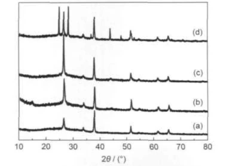
Fig.4 shows the XRD patterns of the as-grown,annealing, and CdCl2-treatment CdS thin films for 90 min of deposition time and FTO thin film.The peaks at 2θ=26.6°,33.8°,37.8°, 51.5°,61.7°,65.6°correspond to(110),(101),(200),(211), (310),(301)planes of SnO2(JCPDS No.46-1088)in the FTO thin film.For the as-grown UCBD-CdS on the FTO thin film, the increases of the intensity ratios at 26.6°and 37.8°are observed.The result indicated a preferred orientation along(111) plane corresponding to the cubic phase of CdS(JCPDS No. 80-0019).18,26For the annealing UCBD-CdS thin film,the intensity ratios at 26.6°and 37.8°further increase.This revealed that the crystallization of small CdS grain was improved.For CdCl2-treatment UCBD-CdS thin films,the peaks at 2θ=24.8°, 28.2°,36.7°,43.8°,47.9°,52.8°appear and correspond to (100),(101),(102),(110),(103),(112)planes of CdS with hexagonal phase(JCPDS No.80-0006).The result demonstrated that the hexagonal phase CdS was formed by CdCl2-treatment procedure.Compared with cubic phase CdS,the hexagonal phase was preferable for thin film solar cells due to its stability.
3.3 Optical characteristic of as-grown,annealing, and CdCl2-treatment UCBD-CdS thin films deposited for 90 min
The direct band gaps of the UCBD-CdS thin films are estimated by extrapolating the linear region of the plot of the absorbance squared(αhν)2versus energy(hν)as show in Fig.5. The direct band gaps of the as-grown,annealing,and CdCl2-treatment UCBD-CdS thin films for 90 min of deposition time are 2.42,2.29,and 2.44 eV,respectively.

Fig.3 SEM images of the UCBD-CdS thin films(a)as-grown;(b)annealing;(c)CdCl2-treatment

Fig.4 XRD patterns for FTO thin film(a)and the UCBD-CdS thin films(b-d)(a)FTO thin film;(b)as-grown;(c)annealing;(d)CdCl2-treatment

Fig.5 (αhν)2vs hν plots for the UCBD-CdS thin films(a)as-grown;(b)annealing;(c)CdCl2-treatment

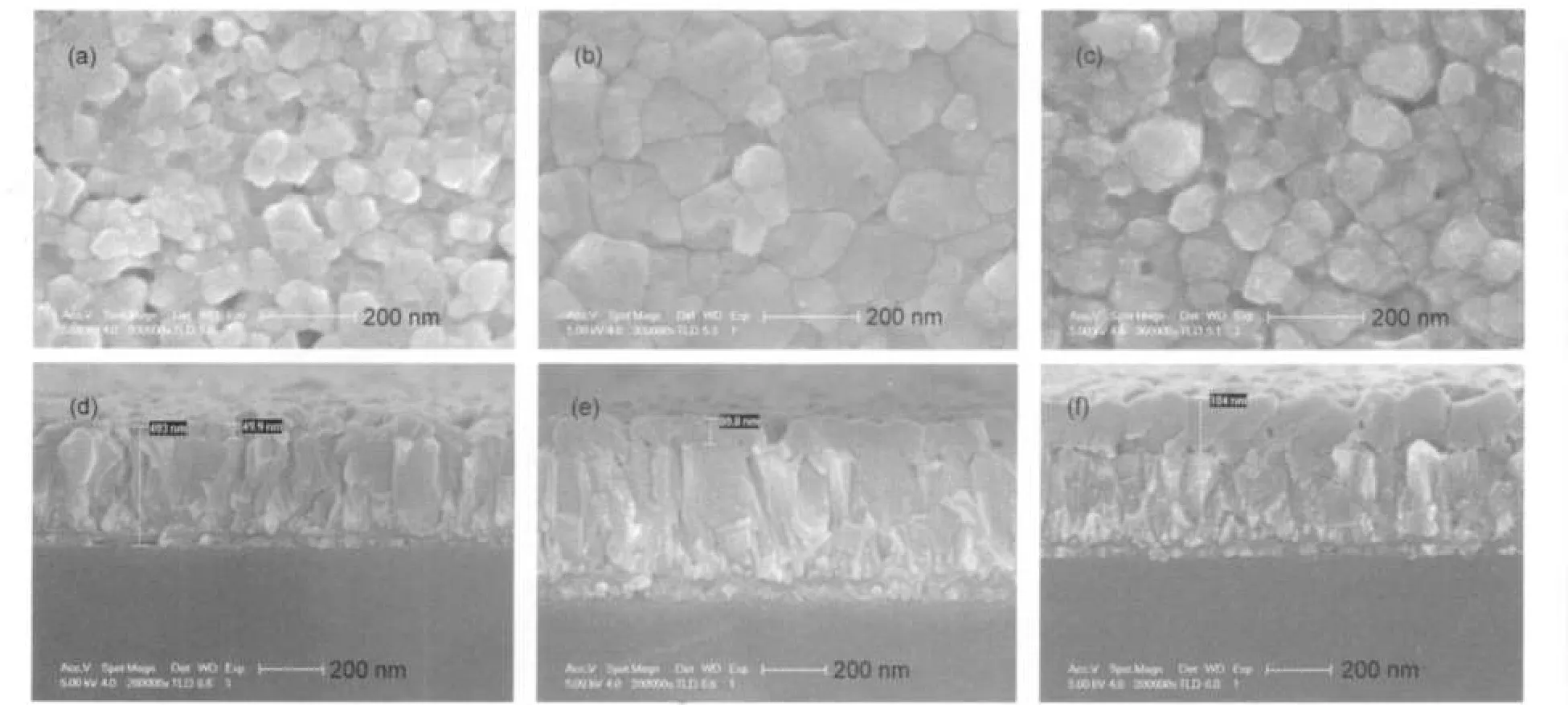
Fig.6 SEM surface and cross-section images of the CdCl2-treatment UCBD-CdS thin films deposited for different time (a,d)20 min;(b,e)40 min;(c,f)60 min
Compared with the as-grown UCBD-CdS thin films,the annealing UCBD-CdS thin films had lower direct band gap.The result should be associated with the crystallization improvement of CdS.The direct band gap of CdCl2-treatment UCBDCdS thin films was higher than that of the annealing ones,and this was due to the appearance of hexagonal phase CdS in the CdCl2-treatment process,which was in good agreement with that observed by SEM and XRD data.The relatively large optical band gap of the CdCl2-treament UCBD-CdS thin films was very important for achieving high energy conversion efficiency in thin film solar cells.
3.4 Influence of deposition time on the grains size and stack denseness of UCBD-CdS thin films
Fig.6 shows the surface and cross-section morphologies of the CdCl2-treatment UCBD-CdS thin films deposited for 20, 40,and 60 min.The grain size of CdS aggregates and thickness of the UCBD-CdS thin films are listed in Table 1.The result is attributed to the ratio of the horizontal to vertical deposition rate.When the deposition time was extended from 20 to 40 min,the thickness of the UCBD-CdS thin films increased from 49.9 to 80.8 nm,lowering the double of 49.9 nm,and the grain size of CdS aggregates increased from 70 to 180 nm. This revealed that the ratio of the horizontal to vertical deposition rate in 20-40 min was higher than that in 0-20 min. When the deposition time was extended from 40 to 60 min,the thickness of the UCBD-CdS thin films increased from 80.8 to 184 nm,heightening the double of 80.8 nm and triple of 49.9 nm,and the grain size of CdS aggregates decreased from 180 to 110 nm.This revealed that the ratio of the horizontal to vertical deposition rate in 40-60 min was lower than that in 20-40 min,which should be because the small CdS grain and the ag-gregates in 40-60 min were deposited on the substrate,the dense UCBD-CdS thin films in 20-40 min.Therefore,the high ratio of the horizontal to vertical deposition rate in 20-40 min was very important to obtain the large grain of CdS aggregates and the dense UCBD-CdS thin films.Moreover,the 80.8 nm thickness of UCBD-CdS thin film was suitable for thin film solar cells as a window layer.It was concluded that the optimal deposition time was 40 min for the CdS thin films using ultrasonic agitation chemical bath deposition.

Table 1 Grain size of CdS aggregates and thickness of the UCBD-CdS thin films
4 Conclusions
In this paper,the influence of annealing and CdCl2-treatment procedure on the surface morphology,crystal structure,and direct band gap of the UCBD-CdS thin films was investigated. The effect of deposition time on the grain size of CdS aggregates and stack denseness in the UCBD-CdS thin films was compared.The result revealed that the small CdS grains in CdS aggregates were melted together and the CdS aggregate size was not changed.The deposition time was very important to obtain the large grain of CdS aggregates and the dense UCBD-CdS thin films.In deposition time of 40 min,the resulting UCBD-CdS thin films were dense and had the 180 nm grain size of CdS aggregates and 80.8 nm of thin film thickness.
(1) Mendoza-Pérez,R.;Aguilar-Hernández,J.;Sastre-Hernández, J.;Ximello-Quiebras,N.;Contreras-Puente,G.;Santana-Rodríguez,G.;Vigil-Galán,O.;Moreno-García,E.;Morales-Acevedo,A.Sol.Energy 2006,80,682.
(2) Morales-Acevedo,A.Sol.Energy 2006,80,675.
(3) Bhattacharya,R.N.;Ramanathan,K.Sol.Energy 2004,77,679.
(4) Liao,C.;Han,J.F.;Jiang,T.;Xie,H.M.;Jiao,F.;Zhao,K.Acta Phys.-Chim.Sin.2011,27,432. [廖 成,韩俊峰,江 涛,谢华木,焦 飞,赵 夔.物理化学学报,2011,27,432.]
(5)Katagiri,H.;Jimbo,K.;Yamada,S.;Kamimura,T.;Maw,W.S.; Fukano,T.;Ito,T.;Motohiro,T.Appl.Phys.Express 2008,1, 041201.
(6)Mahesha,M.G.;Bangera,K.V.;Shivakumar,G.K.Mat.Sci. Semicon.Proc.2009,12,89.
(7) Hernández-Contreras,H.;Mejıá-Garćıa,C.;Contreras-Puente, G.Thin Solid Films 2004,451-452,203.
(8) Raji,P.;Sanjeeviraja,C.;Ramachandran,K.Bull.Mater.Sci. 2005,28,233.
(9)Aguilera,A.;Jayaraman,V.;Sanagapalli,S.;Singh,R.S.; Jayaraman,V.;Sampson,K.;Singh,V.P.Sol.Energy Mater. Sol.Cells 2006,90,713.
(10) Sebastian,P.J.;Calixto,M.E.Thin Solid Films 2000,360,128.
(11)Abou-Ras,D.;Kostorz,G.;Romeo,A.;Rudmann,D.;Tiwari,A. N.Thin Solid Films 2005,480-481,118.
(12) Oliva,A.I.;Castro-Rodríguez,R.;Solís-Canto,O.;Sosa,V.; Quintana,P.;Peña,J.L.Appl.Surf.Sci.2003,205,56.
(13) Moutinho,H.R.;Albin,D.;Yan,Y.;Dhere,R.G.;Li,X.; Perkins,C.;Jiang,C.S.;To,B.;Al-Jassim,M.M.Thin Solid Films 2003,436,175.
(14) Kim,H.;Kim,D.Sol.Energy Mater.Sol.Cells 2001,67,297.
(15) Contreras,M.A.;Romero,M.J.;To,B.;Hasoon,F.;Noufi,R.; Ward S.;Ramanathan,K.Thin Solid Films 2002,403-404,204.
(16) Dongre,J.K.;Nogriya,V.;Ramrakhiani,M.Appl.Surf.Sci. 2009,255,6115.
(17) Sasikala,G.;Thilakan,P.;Subramanian,C.Sol.Energy Mater. Sol.Cells 2000,62,275.
(18) Khallaf,H.;Oladeji,I.O.;Chai,G.Y.;Chow,L.Thin Solid Films 2008,516,7306.
(19) Ramaiah,K.S.;Bhatnagar,A.K.;Pilkington,R.D.;Hill,A.E.; Tomlinson,R.D.J.Mater.Sci.-Mater.El.2000,11,269.
(20) Prabahar,S.;Dhanam,M.J.Cryst.Growth 2005,285,41.
(21) Moualkia,H.;Hariech,S.;Aida,M.S.Thin Solid Films 2009, 518,1259.
(22)Kozhevnikova,N.S.;Rempel,A.A.;Hergert,F.;Magerl,A. Thin Solid Films 2009,517,2586.
(23) Feng,Z.C.;Wei,C.C.;Wee,A.T.S.;Rohatgi,A.;Lu,W.J. Thin Solid Films 2010,518,7199.
(24) Choi,J.Y.;Kim,K.J.;Yoo,J.B.;Kim,D.Sol.Energy 1998,64, 41.
(25)Wan,L.;Bai,Z.Z.;Hou,Z.R.;Wang,D.L.;Sun,H.;Xiong,L. M.Thin Solid Films 2010,518,6858.
(26) Mahanty,S.;Basak,D.;Rueda,F.;Leon,M.J.Electron.Mater. 1999,28,559.
July 14,2011;Revised:September 21,2011;Published on Web:September 29,2011.
Preparation of Large Grain and Dense CdS Thin Films Using Ultrasonic Agitation Chemical Bath Deposition
SHI Cheng-Wu1,2,*CHEN Zhu1,2SHI Gao-Yang1,2SUN Ren-Jie1
(1School of Chemical Engineering,Hefei University of Technology,Hefei 230009,P.R.China;2Key Laboratory of Novel Thin Film Solar Cells,Chinese Academy of Sciences,Hefei 230031,P.R.China)
We deposited CdS thin films onto F-doped SnO2transparent conductive glass by ultrasonic agitation chemical bath deposition(UCBD).The influence of the annealing and CdCl2-treatment on the surface morphology,crystal structure,and direct band gap of the UCBD-CdS thin films was investigated. The effect of deposition time on the grain size of the CdS aggregates and the stack denseness of the UCBD-CdS thin films was compared.The results reveal that the small grains in the CdS aggregates were melted together and the CdS aggregate size did not change in the UCBD-CdS thin films after the CdCl2-treatment procedure.It is interesting that the ratio of the horizontal to vertical deposition rate varied with deposition time over the deposition period of the UCBD-CdS thin films.The deposition time was very important to obtain large CdS aggregate grains and dense UCBD-CdS thin films.Over a deposition time of 40 min the resulting UCBD-CdS thin films were dense and had a 180 nm grain size of CdS aggregates and a 80.8 nm of thin film thickness.The large-grained and dense UCBD-CdS thin films were suitable for thin film solar cells as a window layer.
CdS thin film;Ultrasonic agitation;Chemical bath deposition;Deposition time; Annealing;CdCl2-treatment
10.3866/PKU.WHXB20112821
∗Corresponding author.Email:shicw506@gmail.com;Tel:+86-551-2901450.
The project was supported by the National Natural Science Foundation of China(51072043),National Key Basic Research Program of China(973) (2011CBA00700),Anhui Province Science and Technology Plan Project of China(2010AKND0794),College Natural Science Foundation ofAnhui Province,China(KJ2010A266),and Undergraduate Innovation Fund of Hefei University of Technology,China(cxsy102084).
国家自然科学基金(51072043),973计划重大科学问题导向项目(2011CBA00700),安徽省年度重点科研计划项目(2010AKND0794),安徽省高校自然科学基金(KJ2010A266)及合肥工业大学学生创新基金(cxsy102084)资助项目
O646;TM914.4+2

