整形高功率激光装置的任意电脉冲发生器设计
刘 辉,刘百玉,白永林,欧阳娴,缑永胜,郑锦坤
(1.中国科学院西安光学精密机械研究所,超快光电诊断技术重点实验室,陕西西安710119;2.中国科学院西安光学精密机械研究所,瞬态光学与光子技术国家重点实验室,陕西西安710119;3.中国科学院研究生院,北京100049)
整形高功率激光装置的任意电脉冲发生器设计
刘 辉1,3,刘百玉2,白永林2,欧阳娴2,缑永胜2,郑锦坤1,3
(1.中国科学院西安光学精密机械研究所,超快光电诊断技术重点实验室,陕西西安710119;2.中国科学院西安光学精密机械研究所,瞬态光学与光子技术国家重点实验室,陕西西安710119;3.中国科学院研究生院,北京100049)
1 Introduction
In the mid of 1960s,the concept of achieving the fusion between deuterium and tritium by a high power laser pulse is put forward.The laser heats the pellet instantly and the generated inertia recoil produces high temperature and high pressure,which leads to nuclear fusion to occur.This process is called Inertia Confinement Fusion(ICF).The achievement of ICF needs that the ablation pressure resulting from the laser pulse irradiating the pellet must increase according to certain rules.Therefore,there are high requirements for a laser pulse shape system.The new ICF driver demands that multi-channel laser pulses must be with arbitrary shaping ability,besides each channel′s waveform is the same so as to make power balance.The arbitrary laser pulse can be acquired by modulating the Q-switched pulse output from a master oscillator with pockel cells or optical waveguide modulators.
The advanced approach to adjust the laser pulse shape is to utilize the integrated optics technology[1,2].By injecting the shaping electrical pulse into the optical waveguide modulator,and then the laser pulse shape can be determined by the electrical pulse.The arbitrary waveform generator takes advantage of pure electronic devices with simple structure,excellent specifications,dependable performance,and the lower cost.It can generate an ultrawide band low voltage pulse with high stability.For the reason that the laser driver shape in ICF is particular with the narrow width and wide dynamic range,it is the key technology to generate this kind of electrical pulse.Consequently,the research for generating arbitrary waveform technology plays a significant role in the ICF driver design.
2 Design of pulse shaping circuit
2.1 The basic unit circuit

Fig.1 Principle of generating unit pulse.
The basic unit circuit is show in Fig.1.The on-off state of GaAs FET is determined by triggering pulse and the direct current bias together.The pinch-off voltage of GaAs generally is~2.2 V[3]. When the triggering pulse does not come to the gate port,the GaAs is on off state which is can be shown in Fig.1(a).At the time that the triggering pulse propagates to the gate,the voltage that the pulse amplitude and the bias add together is higher than pinch-off value.As is shown in Fig.1(b),the GaAs is on an open state.There is a basic unit electrical pulse with same amplitude and waveform but opposite polarity as triggering pulse.This unit pulse propagates along the transmission line into two different directions.In order to eliminate the reflection generating from the generated pulse,a 50 Ω load is set to assimilate the left-travel sub-pulse.The righttravel sub-pulse as a basic unit pulse makes a part of the shaping electrical pulse.
2.2 Pulses accumulation
Fig.2 demonstrates the process ofeach sub-pulse accumulating together[4].Each GaAs FET consists of a basic unit circuit.When the triggering pulse arrives to the first GaAs,it is in an on state and a unit pulse is obtained propagating forward along transmission line.After a certain delay time,the triggering pulse comes to the second GaAs,it is open too.We obtain the second unit pulse which can be accumulated with the first one to form a widther pulse.The delay time between the adjacent unit pulses is designed by controlling the length difference of pulse transmission line.The triggering pulse triggers GaAs FETs in turn and generates several independent basic unit pulses to accumulate together.Thus, the shaping electrical pulse is obtained.

Fig.2 Pulses accumulating theory.
3 Pulse transmission line design
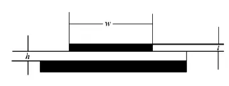
At present,the micro-strip technology is widely used in the transmission line field which can be executed by a gerber file format.Furthermore,it can be integrated with some passive and active microwave devices.With the quasi-TEM mode[5],the phase velocity, propagation constantand characteristic impedance of micro-strip can be obtained by analyzing quiescent or quasi-quiescent wave equations.In the ultra-fast pulse generator, the micro-strip technology is utilized in signal generating and transmitting circuits,which is taken for reducing the effects that high-frequency distribution parameters result in.Thus,the front-edge and the end-edge of electrical pulse can be improved[6].The structure of micro-strip line is shown in Fig.3.A strip single line and the ground plane are separated by the dielectric.The characteristic impedance of microstrip is controllable by altering the copper thickness and the width of signal line or the width of dielec-tric.And the design precision is within the scope of 5%.

Fig.3 Micro-strip line structure
The parameters of micro-strip are given in Fig. 3,therefore the characteristic impedance can be computed according to the formula below[7]


In the formula(1)and(2),εris the relative dielectric constant of the material that is made of PCB board;h is the thickness of the dielectric layer;W and t are the width and thickness of the zonal wire,respectively.In the design,50 Ω micro-strip line is used for generating ultra-fast electrical pulse. According to formula(1),selection to high frequency PCB material and the width of micro-strip can be realized;based on formula(2),we can confirm the length of delay line.
The propagation delay time is
4 Experimental results and analysis
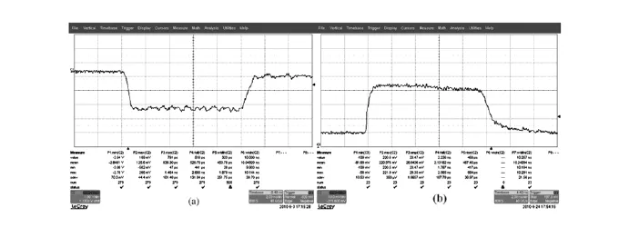
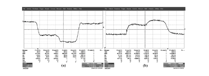
The AWG adopting GaAs FET as switch device takes full advantage of voltage controlling current and onoff characteristics.Each channel of basic unit pulse amplitude is controlled by adjusting the corresponding gate bias.The multi-channel unit pulses with different amplitudes are added independently,and the dif-form electrical pulses waveform are generated.And then,injecting the electrical pulse into optical waveguide modulator,a laser pulse with the same waveform as electrical one is output.The experiment results are shown in Figs.4 and 5;(a)is the electrical pulse and the(b)is the laser pulse output from an optical waveguide modulator.They are with the same shape but different polarities.
The amplitude of pulse generated by electrical generator is too low to apply to the optical waveguide modulator.Therefore,an ultra-wide bandwidth voltage amplifier is used at the end of output interface to enlarge the signal pulse.Finally,the shaped and amplified electrical pulse is applied to the electrical waveguide modulator and the exactly same shape optical pulse is generated and applied to the high-power laser shaping system.The experiment results are satisfied.

Fig.4 Square waveform.

Fig.5 Ladder waveform.
5 Conclusions
An ultra-wide bandwidth electrical shaping pulse generator consisting of GaAs and micro-strip line is proposed. The generatorcan generate arbitrary waveform pulse within the width of 10 ns and amplitude of 5 V.The pulse is applied to the optical waveguide modulator and the ideal shape optical pulse is generated.The electrical shaping technology can be also used in radar communication,radar positioning,information ware,complex analog radar signals and optical communications areas.
Reference:
[1]曹霞,谢新龙,王治国,等.ICF系统中波导调制器脉冲整形技术[J].上海交通大学学报,2000,34(8):1108-1111.
CAO X,XIE X L,WANG ZH G,et al..Laser pulse forming technique by using waveguide modulator in ICF system[J]. J.Shanghai Jiao Tong University,2000,34(8):1108-1111.(in Chinese)
[2]谢兴龙,陈绍和,周良智,等.利用波导调制器实现连续可调任意整形激光脉冲[J].光学学报,1997,17(4):393-398.
Xie X L,CHEN SH H,ZHOU L L,et al..Continuously tunable system for arbitrary forming of laser pulse using intergrated LiNbO3waveguide modulator[J].Acta Optica Sinica,1997,17(4):393-398.(in Chinese)
[3]李东,刘百玉,刘进元,等.用于高功率激光装置中的电脉冲整形系统[J].光子学报,2005,34(9):1304-1306.
LI D,LIU B Y,LIU J Y,et al..Electrical pulse-shaping system on the high power laser system[J].Acta Photonica Sinica,2005,34(9):1304-1306.(in Chinese)
[4]BURKHART S C.Voltage-controlled MESFET pulse shape generator[R].UCRL-ID-116054.CA:Lawrence Livermore National Laboratory,1994.
[5]POLZAR D M.Microwave Engineering[M].Hamilton:Wiley Hamilton Printing,2005.
[6]王玲.微带传输线在高速脉冲发生器中的应用[J].核电子学与探测技术,2005,25(1):67-69.
WANG L.The application of microstrip transmission line in a high-speed pulse generator[J].Nuclear Electronics and Detection Technol.,2005,25(1):67-69.(in Chinese)
[7]徐兴福.ADS2008射频电路设计与仿真实例[M].北京:电子工业出版社,2009.
XUE X F.ADS2008 RF Circuit Design and Simulate Eχamples[M].Beijing:Publishing House of Electronics Industry,2009.(in Chinese)
[8]BURKHART S C,WILCOX R B.Arbitrary pulse shape synthesis via nonuniform transmission lines[J].IEEE Trans Microwave Technol.,1990,38(10):1514-1518.
Author′s biography:LIU Hui(1986—),male,born in Linyi Shandong Province.He received his B.S degree in electrical engineering from South-Central University for Nationalities in 2008.Now he is working for M.S degree in Xi'an Institute of Optics and Precision Mechanics of CAS.His research interest is ultra-bandwidth pulse shaping technology.E-mail:liuhui@opt.ac.cn
LIU Bai-yu(1964—),male,born in Weinan Shanxi Province,researcher.He received his B.S degree from Tsinghua University in 1986.At present,he is a researcher in Xi'an Institute of Optics and Precision Mechanics of CAS.His research interest is ultrafast electronics.E-mail:liubaiyu@opt.ac.cn
BAI Yong-lin(1972—),male,born in Baoji Shaanxi Province,researcher.He received his B.S degree from Northwest University in 1996,and got his Ph.D from Xi'an Institute of Optics and Precision Mechanics of CAS.At present,he is a researcher in Xi′an Institute of Optics and Precision Mechanics of CAS.His research interest is FPGA exploration and ultrafast diagnosis.E-mail:baiyonglin@opt.ac.cn
Design of arbitrary waveform generator for shaping high power laser system
LIU Hui1,3,LIU Bai-yu2,BAI Yong-lin2,OUYANG Xian2,GOU Yong-sheng2,ZHENG Jin-kun1,3
(1.Key Laboratory of Ultra-fast Photoelectric Diagnostics Technology,Xi′an Institute of Optics and Precision Mechanics,Chinese Academy of Sciences,Xi′an 710119,China;2.State Key Laboratory of Transient Optics and Photonics,Xi′an Institute of Optics and Precision Mechanics,Chinese Academy of Sciences,Xi′an 710119,China;3.Graduate University of Chinese Academy of Sciences,Beijing 100049,China)
In order to improve the output power of a laser pulse in the Inertia Confinement Fusion(ICF)system,an Arbitrary Generator(AWG)is designed to shape the laser pulse with an ideal condition.The ultranarrow pulse is used to trigger the GaAs Field Effect Transistor(FET)to generate multiple negative pulses. The different time delays for each pulse are introduced by transmitting it through an analog time delay wire.Finally,a micro-strip line is obtained to couple the pulses and to get the overlapped pulse shape.The gate bias on FET is used to determine the magnitude of pulse,so the arbitrary pulse is gotten by overlapping the multiple pulses with various magnitudes and time delays.To satisfy the high amplitude requirement of electrical pulse for the ICF system,an ultra-broad bandwidth and voltage tunable amplifier is applied to the output signals and the pulse amplitude is adjustable.The designed AWG generates a pulse waveform with amplitude between 0 and 5 V,pulse width less than 10 ns and a square waveform rising edge in 520 ps,falling edge in 790 ps.The experiment shows the shaped laser pulse is obtained based on the shaping electrical pulse.
Arbitrary Waveform Generator(AWG);high power laser;micro-strip line;GaAs Field Effect Transistor(FET)
基于GaAs场效应管电压控制电流和开关的特性,设计了一种任意电脉冲发生器,并成功应用于激光脉冲整形装置。该电脉冲发生器利用超宽带窄脉冲触发多个GaAs场效应管,产生多路负脉冲,通过模拟延时线依次将各路负脉冲延迟一定时间后经微带线耦合输出多路负脉冲叠加的波形;通过多路不同幅度的脉冲堆积效应来获得形状任意可调的整形电脉冲。为了满足惯性约束聚变(ICF)实验中对电脉冲幅度不能过小的要求,在电路的输出端接入增益可调的超宽带电压放大器,使脉冲幅度达到实验要求。利用设计的任意电脉冲发生器实现了脉冲幅度0~5 V可调、脉宽0~10 ns可调、时域调节精度为330 ps,整形方波脉冲下降沿为330 ps、上升沿为240 ps。实验结果表明,将产生的电脉冲注入光波导调制器,可获得理想形状的整形激光脉冲,提高激光脉冲的输出能量。
任意波形发生器;高功率激光;微带线;GaAs场效应管
TN243
A
1674-2915(2011)01-0060-06
2010-08-16;
2010-10-23

