
E mission and capture characteristics of deep hole trap in n-GaN by optical deep level transient spectroscopy
2024-03-15 04:31:52JinSuiJiaxiangChenHaolanQuYuZhangXingLuandXinboZou
Journal of Semiconductors 2024年3期
Jin Sui ,Jiaxiang Chen ,Haolan Qu,Yu Zhang,Xing Lu,and Xinbo Zou†
1School of Information Science and Technology,ShanghaiTech University,Shanghai 201210,China
2Shanghai Institute of Microsystem and Information Technology,Chinese Academy of Sciences,Shanghai 200050,China
3School of Microelectronics,University of Chinese Academy of Sciences,Beijing 100049,China
4School of Electronics and Information Technology,Sun Yat-sen University,Guangzhou 510275,China
Abstract: Emission and capture characteristics of a deep hole trap (H1) in n-GaN Schottky barrier diodes (SBDs) have been investigated by optical deep level transient spectroscopy (ODLTS).Activation energy (Eemi) and capture cross-section (σp) of H1 are determined to be 0.75 eV and 4.67 × 10⁻¹⁵ cm2,respectively.Distribution of apparent trap concentration in space charge region is demonstrated.Temperature-enhanced emission process is revealed by decrease of emission time constant.Electricfield-boosted trap emission kinetics are analyzed by the Poole-Frenkel emission (PFE) model.In addition,H1 shows point defect capture properties and temperature-enhanced capture kinetics.Taking both hole capture and emission processes into account during laser beam incidence,H1 features a trap concentration of 2.67 × 1015 cm-3.The method and obtained results may facilitate understanding of minority carrier trap properties in wide bandgap semiconductor material and can be applied for device reliability assessment.
Key words: GaN;deep level transient spectroscopy;minority carrier trap;time constant;trap concentration
1.Introduction
Gallium nitride (GaN) has been considered as a promising material for power electronics[1]and optoelectronic devices,e.g.,light emitting diodes (LEDs)[2],photodetectors[3],and solar cells[4],due to its wide energy bandgap,high electron mobility,and high thermal conductivity.However,traps in semiconductor materials may significantly impact the conductive properties and operational performance of semiconductor devices and related electronics[5-8].Therefore,understanding the nature of traps in GaN devices holds both scientific and practical significance for improving GaN material quality and associated device efficiency.
There have been some investigations on the properties of traps in GaN-based devices.Angelottietal.have previously extracted a shallow-level trap in a GaN radio frequency(RF) HEMT by drain current transient (DCT) analysis[9].Using deep level transient spectroscopy (DLTS),Hierroetal.determined the carrier capture kinetics of electron traps in n-GaN[10].DLTS holds the features of high sensitivity,high resolution,non-destructive analysis,and so on.DLTS has been performed on a variety of GaN-based devices such as Schottky barrier diodes (SBDs)[11],p-n and p-i-n junctions[12].These studies have revealed various traps in GaN films,which are grown by various methodologies involving metal-organic chemical vapor deposition (MOCVD)[13,14],hydride vapor phase epitaxy (HVPE)[15],and molecular beam epitaxy(MBE)[16].Our previous work has demonstrated several majority carrier (electron) traps in n-GaN SBDs by DLTS technique using electrical pulses[17].However,during the electrical filling pulse,a large number of majority carriers are injected in the n--GaN layer.Thus,the DLTS signal is dominated by majority carrier traps,making the signature of minority carrier traps in the n--GaN layer remain undetected.Minority carrier traps have significant technical implications due to their impact on carrier lifetime in some bipolar devices[18].However,study on minority carrier traps in GaN materials is relatively challenging and limited.
The minority carrier traps could be investigated using optical deep level transient spectroscopy (ODLTS)[19,20]or minority carrier transient spectroscopy (MCTS)[21,22]to boost the minority carrier concentration.Polyakovetal.identified hole traps with activation energies of 0.7 and 0.9 eV in n-GaN SBDs grown on sapphire substrates using ODLTS[23,24].Amoretal.also revealed a hole trap characterized by activation energy of 0.76 eV utilizing DLTS,but only capture crosssection and emission time were extracted[20].There are still some issues that need to be addressed to thoroughly understand the minority carrier trap properties in GaN materials.(i)There is still insufficient research on the detailed emission mechanism for deep hole traps,which have a significant contribution in device properties such as conductivity compensation and non-equilibrium carrier recombination[25,26].There is scarce information on electric-field (E) dependent emission kinetics for minority carrier traps in GaN-based materials.The electric-field in the depletion region should be taken into account since it can substantially affect the emission rate[27].(ii) There remains a lack of quantitative analysis of the capture kinetics of deep hole traps.A comprehensive investigation into the capture kinetics of traps can reveal profound insights into the physical characteristics of defects in GaN materials[28].
In this article,we have studied emission and capture kinetics of minority carrier (hole) trap H1 in n-GaN SBD on sapphire substrate using ODLTS.Temperature-scanning ODLTS results reveal a hole trap H1 identified with activation energy of 0.75 eV and capture cross-section of 4.67 × 10⁻¹⁵cm2.The profile of the apparent trap concentration of H1 in the space charge region has been investigated.Isothermal ODLTS for scanning measurement time (TW) and capacitance transient studies at different temperatures suggest temperatureenhanced carrier emission process and electric-fieldenhanced carrier emission kinetics.The capacitance transient amplitude trends corresponding to various optical pulse width (tp) reveal the point defect type of H1 and the temperature-dependent capture kinetics.These results will provide valuable insights into the properties of minority carrier traps in GaN and contribute to the development of GaN-based devices with enhanced performance and reliability.
2.Experimental details
Fig.1 (a) depicts a cross-section diagram of GaN SBD in this study.The GaN SBD was prepared by MOCVD on a 2-inch sapphire substrate.The epi-layer structure started with GaN buffer layer with 1-μm thickness and continued with n+-GaN layer with thickness of 1.8μm and electron concentration of 5 × 1018cm-3.Subsequently,an unintentionally-doped n--GaN layer was deposited with thickness of 5.8μm and carrier concentration of 5.3 × 1015cm-3.Following etching and sidewall passivation using SiNX,a deposition of Ti/Al/Ni/Au was performed on the exposed n+-GaN layer as the cathode.Ti/Al/Ni/Au Ohmic contact underwent annealing at 850 ℃ for 30 s.On the mesa,a layer of Ni/Au with a diameter of 400μm was deposited as the anode,and the Ni/Au Schottky contact remained unannealed.The ODLTS measurement was conducted utilizing the FT 1230 high energy resolution analysis deep level transient spectroscopy (FT 1230 HERA-DLTS) system (PhysTech) equipped with a 10 mW laser with 405 nm wavelength.
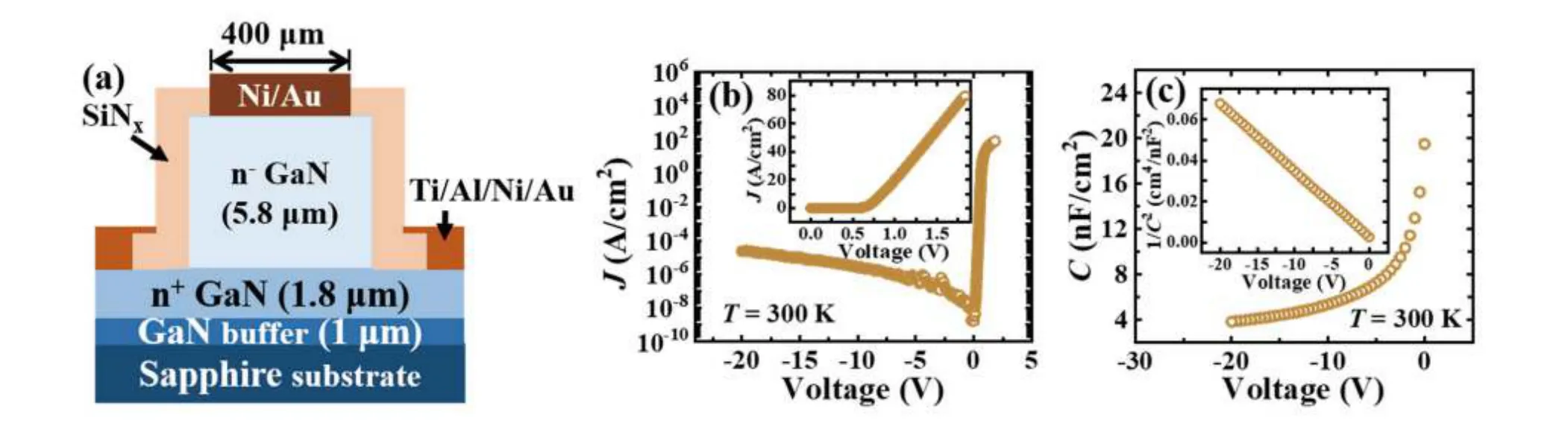
Fig.1.(Colour online) (a) A cross-section diagram of a GaN quasi-vertical SBD under experimentation.(b) Forward and reverse J—V characteristics at 300 K presented by logarithmic scale.Inset: forward J-V characteristics at 300 K in linear scale.(c) C—V characteristics at 300 K.Inset: 1/C2—V curve at 300 K.
3.Results and discussion
Fig.1(b) presents the forward and reverse current density—voltage (J—V) characteristics of the GaN SBD at 300 K.The inset of Fig.1(b) represents forwardJ—Vcharacteristics in linear scale.The threshold voltage (Vth) was identified as 0.65 V at 300 K with a current density of 1 A/cm2.Meanwhile,Fig.1(c) depicts the capacitance—voltage (C—V) characteristics of the GaN SBD at 300 K.The frequency and AC amplitude of theC—Vtest were 1 MHz and 50 mV,respectively.As indicated in the inset of Fig.1(c),1/C2—Vcharacteristics are plotted and present a linear relationship,suggesting that the carrier concentration is uniformly distributed.The carrier concentration (NS) was calculated as 4.59 × 1015cm-3from the slope of 1/C2—V(Eq.(1)).
whereqis the elementary charge,εris the relative permittivity of GaN,ε0is vacuum permittivity,andAis the anode area[11].
Temperature-scanning ODLTS spectra was employed to extract trap properties in n--GaN layer[29,30].Fig.2(a) shows energy band diagrams of capture and emission process for hole trap during the ODLTS measurement.Featuring a subbandgap wavelength of 405 nm,the optical pulse provides enough energy to activate the holes.A substantial number of holes are photon-excited and captured by hole trap in the n--GaN layer during optical filling pulse period.At the end of filling period,the occupied hole trap starts to thermally emit holes for measurement period[31].ODLTS measurement was conducted with a reverse bias (UR) of -6 V,atpof 1 s,and aTWof 10 s.In Fig.2(b),the inverted ODLTS spectra displays a prominent signal valley at approximately 315 K,representing a minority carrier trap.Upon application ofURof -6 V,the space charge region is located in the n--GaN layer,accordingly,it is confirmed to be a hole trap (H1).Fig.2(c) exhibits Arrhenius plot of the hole trap H1 resulting from the temperature-scanning ODLTS spectra.The activation energy (Eemi)and capture cross-section (σp) of the hole trap H1 were determined to be 0.75 eV and 4.67 × 10⁻¹⁵cm2,respectively,through the Arrhenius relation[30,32].Theσpby default represents the optical capture cross-section extracted by ODLTS[33].

Fig.2.(Colour online) (a) Energy band diagrams of hole trap in GaN for (1) capture and (2) emission process.(b) Inverted temperature-scanning ODLTS spectra.(c) Arrhenius plot for hole trap H1.(d) Apparent trap concentration profile versus depletion region width.
Fig.2(d) illustrates apparent trap concentration (NTa) profile versus depletion region width (WR) at 315 K,obtained from the isothermal ODLTS results for scaningUR.WRwas determined fromC—Vcharacteristics at 315 K by the relation[34]:
Meanwhile,apparent trap concentration (NTa) at differentUR(that is,differentWR) is given by[22]
whereΔCis the capacitance transient amplitude,CRis the steady-state capacitance atUR,andNSis the net carrier concentration calculated from theC—Vcharacteristics at 315 K by Eq.(1).ΔCandCRat differentURwere obtained from isothermal ODLTS measurement for scanningUR.For isothermal ODLTS measurement,tpwas set to 1 s to ensure that all traps were filled.The increase ofNTawith extendingWRis associated with the quick carrier recombination effect at the depletion region boundary[22].
Fig.3(a) presents the isothermal ODLTS spectra of trap H1[35,36],which was performed from 315 to 343 K withURof-6 V andtpof 1 s.The emission time constants (τe) were determined by extracting valley position from isothermal ODLTS spectra.As the temperature increases,the signal valley associated with trap H1 shifts towards a lowerTW,indicating a decrease ofτe.Theτeof trap H1 at various temperatures are displayed in Fig.3(b).It's noteworthy that theτeof H1 consistently decreased from 8.95 s at 315K to 0.74 s at 343 K,suggesting an increase of the emission rate at higher temperatures.
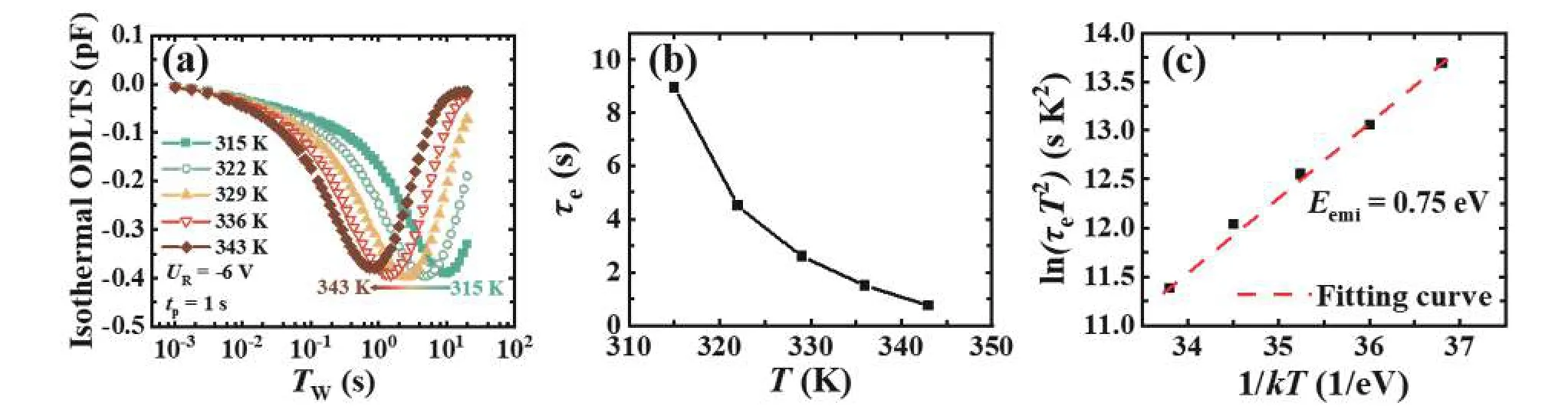
Fig.3.(Colour online) (a) Isothermal ODLTS spectra for scanning TW with fixed UR of -6 V and tp of 1 s from 315 to 343 K.(b) τe derived by isothermal ODLTS at different temperatures.(c) Arrhenius plot of trap H1 extracted from temperature-dependent τe.
As indicated in Fig.3(c),the relationship betweenτeand temperature can be fitted by Eq.(4)[37]:
whereγis a constant relating to effective hole mass.From the slope and intercept of the Arrhenius plot in Fig.3(c),the activation energy of trap H1 is determined to be 0.75 eV with a capture cross-section in the order of 10-15cm2as well,which is consistent with the results obtained by Fig.2(c).
Fig.4(a) illustrates correspondence between emission time constant (τe) and electric-field extracted from capacitance transient spectra with differentURat three different temperatures: 315,322,and 329 K.τedecreased significantly with an increased electric-field at each temperature,which can be attributed to a reduction in the apparent thermal activation energy with the electric-field.It is also observed thatτedecreased markedly with elevated temperature,which shows agreement with the conclusion in Fig.3(b).
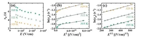
Fig.4.(Colour online) (a) Electric-field-dependent τe of trap H1 extracted from capacitance transient spectra from 315 to 329 K.The ln(ep) of trap H1 as a function of (b) E2 and (c) E1/2 from 315 to 329 K.Black dotted lines are linear fitting curves.
The relationship between the logarithm of the emission rate (ep) and the square of the electric-field (E2) was illustrated in Fig.4(b).It was observed that a linear fit was not feasible,suggesting that the enhancement cannot be solely attributed to a phonon-assisted tunneling process.However,ln(ep) is plotted as a function of the square root of the electric-field (E1/2),as shown in Fig.4(c).The linear fitting of the relationship shows that the enhancement process can be adequately described by Poole-Frenkel emission (PFE) process,which can characterize the progression ofepwithEfor H1 at these temperatures[38].
Fig.5(a) displays normalized capacitance transient amplitude of trap H1 as a function oftpat various temperatures.Astpincreases,capacitance transient amplitude (ΔC) first increases rapidly,which is related to the increment of the population of filled traps.Astpreaches a sufficiently long duration,all traps are completely filled,leading to saturation ofΔC.
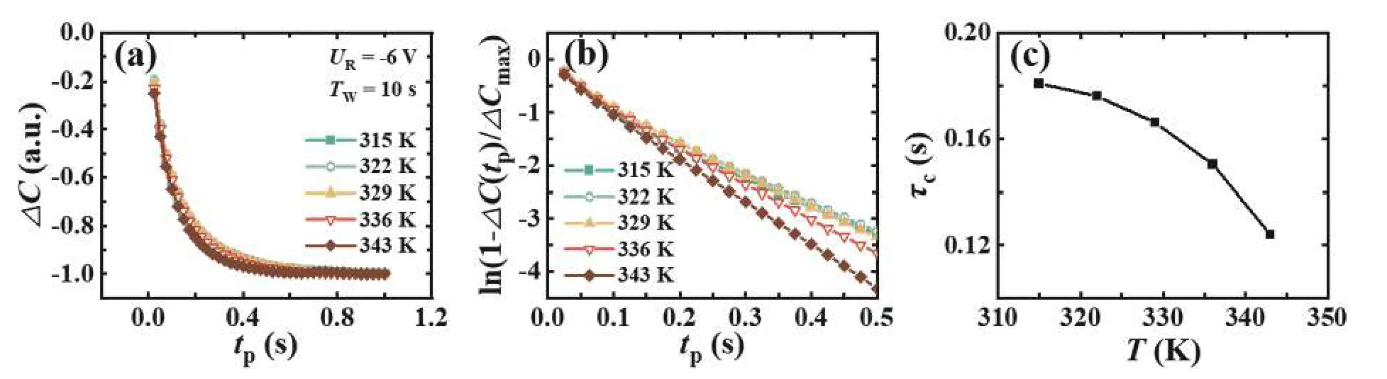
Fig.5.(Colour online) (a) Normalized capacitance transient amplitude as a function of tp.(b) Capacitance transient amplitude increases exponentially with tp.(c) τc from 315 to 343 K.
As illustrated in Fig.5(b),the relationship betweenΔCandtpcould be expressed as[39]
whereΔCmaxis the saturated capacitance transient amplitude andτcis apparent capture time constant.It is observed that the curves of lnversustpexhibit good linearity at several temperatures.Therefore,H1 is regarded as a point defect rather than an extended defect in terms of the excellent linear trend of curves in Fig.5(b)[40].From slope of linear fitting curve in Fig.5(b),τcas a function of temperature was extracted,as shown in Fig.5(c).From 315 to 343 K,τcwas reduced from 0.18 to 0.12 s,which demonstrates a thermally enhanced capture property.Compared with capture time constants reported for majority carrier trapping process in the literatures[9,10],theτcof minority carrier trap shows a much larger value.This is related to the small minority carrier concentration in the n-GaN material,which lower the probability of the holes getting captured,leading to a largeτcfor hole trap (H1)[41].In addition,smallσp(4.67 × 10⁻¹⁵cm2) of H1 also suggested weaker capability of the hole trap to capture holes,and thus a relatively large capture time constant.The value ofτcfor H1 in this work is actually comparable to time constant (0.36 s) extracted for a hole trap (EV+0.86 eV)in n-GaN using isothermal MCTS[42].It is worth noting thatτcis not equal to the time required for traps to be completely filled.Theτcsignifies the time it takes for the unfilled trap concentration to decrease to 1/etimesNTa,shorter than the time taken for traps to be completely occupied[32].
The isothermal ODLTS spectra,depicted as a function ofTWin Fig.3(a) andtpin Fig.5(b),can be utilized to estimate the trap concentration.For instance,atT=315 K,theτcfor the exponential relationship between theΔCandtpis estimated to be 0.18 s.The trapped hole concentration (pt) can be computed considering the simultaneous events of hole capture and emission during laser beam incidence,according to
wherecpis the hole capture coefficient,epis the hole emission rate,pis the hole concentration,andNTis the trap concentration[43].Under the assumption of a uniform hole concentration within the depletion region during laser beam incidence,the value ofcppcan be computed as 5.44 s-1.This calculation utilizes the determined value ofepas 1/8.95 s-1,obtained from Fig.3(a),and (cpp+ep) as 1/0.18 s-1,derivedfrom Fig.4(b).By employing the saturated capacitance transient amplitudeΔCmaxand the corresponding relation[42]
NTis obtained to be 2.67 × 1015cm-3.With the incident laser beam on,holes and electrons undergo optical emission,resulting in a reduction ofpt.Consequently,the obtained value ofNTmay be underestimated.The result obtained from Eq.(7)are slightly larger than that obtained in Eq.(3),indicating the existence of a large trap concentration for hole trap H1.Trap concentration of H1 is one to two orders of magnitude larger than the concentration of majority carrier (electron) traps in our previous work[17].
Table 1 summarizes the trap characteristics of hole trap H1 in this work and other traps in literatures.The smallerσpindicates that the hole trap in the device is relatively incapable of trapping holes.Polyakovetal.have reported that the trap concentration can be reduced by three orders of magnitude by changing the device fabrication process conditions[23].Corresponding to the different characteristics of the devices,H1 can be detected in n-GaN using different measurement techniques,i.e.,MCTS[44],ODLTS[23],DLTS[20],and test conditions.H1 can be observed for materials grown by HVPE and MOCVD methods,suggesting that it is an extensive-existed defect[20,23].In this work,for the first time,the emission mechanism of H1 was determined to comply with the Poole-Frenkel emission model.
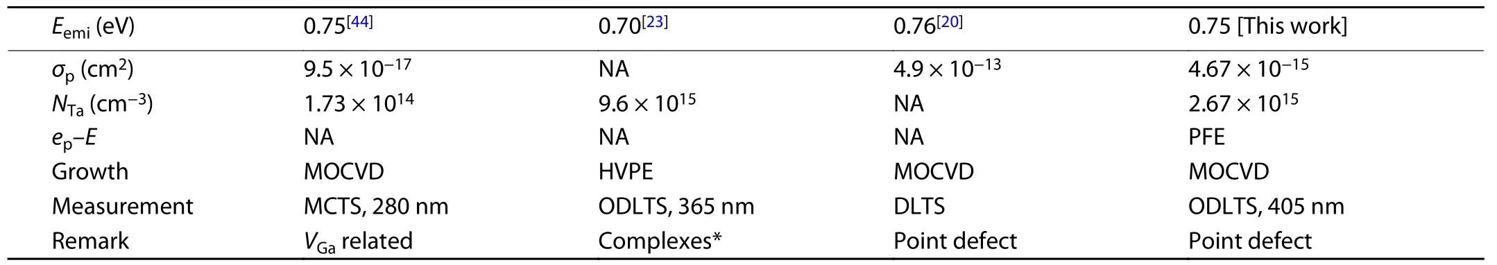
Table 1.Comparison with other published comparable hole trap in n-GaN.
4.Conclusion
In conclusion,trap characteristics of a minority carrier(hole) trap in n-GaN SBD grown by MOCVD have been thoroughly analyzed using ODLTS.The hole trap (H1) characterized byEemiof 0.75 eV andσpof 4.67 × 10⁻¹⁵cm2is considered to be a point defect.Temperature-enhanced emission and capture kinetics are investigated as the temperature increases from 315 to 343 K.This is evidenced by a significant reduction of emission time constant from 8.95 to 0.74 s and a gradual decrease of apparent capture time constant from 0.18 to 0.12 s.The emission process of H1 is found to be accelerated by electric-field,which can be well described by Poole-Frenkel emission model.In addition,the hole trap exhibits a high trap concentration of 2.67 × 1015cm-3,taking into account that hole trapping and emission processes occur simultaneously during luminescence.These results regarding the specific properties of the deep-level trap in GaN may contribute to the advancement of GaN devices towards improved performance and reliability in power and RF electronics.
Acknowledgments
This work was supported by ShanghaiTech University Startup Fund 2017F0203-000-14,the National Natural Science Foundation of China (Grant No.52131303),Natural Science Foundation of Shanghai (Grant No.22ZR1442300),and in part by CAS Strategic Science and Technology Program(Grant No.XDA18000000).
 Journal of Semiconductors2024年3期
- Journal of Semiconductors的其它文章
- 2D black arsenic phosphorous
- Visible-to-near-infrared photodetectors based on SnS/SnSe2 and SnSe/SnSe2 p-n heterostructures with a fast response speed and high normalized detectivity
- G Hz photon-number resolving detection with high detection efficiency and low noise by ultra-narrowband interference circuits
- Behavior of exciton in direct-indirect band gap AlxGa1-xAs crystal lattice quantum wells
- A novel one-time-programmable memory unit based on Schottky-type p-GaN diode
- P hysical insights into trapping effects on vertical GaN-on-Si trench MOSFETs from TCAD