
11.2 W/mm power density AlGaN/GaN high electron-mobility transistors on a GaN substrate
2024-03-04 05:48:36YanshengHuYuangangWangWeiWangYuanjieLvHongyuGuoZhirongZhangHaoYuXuboSongXingyezhouTingtingHanShaoboDunHongyuLiuAiminBuandZhihongFeng
Journal of Semiconductors 2024年1期
Yansheng Hu, Yuangang Wang, Wei Wang, Yuanjie Lv, Hongyu Guo, Zhirong Zhang, Hao Yu, Xubo Song,Xingye zhou, Tingting Han, Shaobo Dun, Hongyu Liu, Aimin Bu, and Zhihong Feng
National Key Laboratory of Solid-State Microwave Devices and Circuits, Hebei Semiconductor Research Institute, Shijiazhuang 050051, China
Abstract: In this letter, high power density AlGaN/GaN high electron-mobility transistors (HEMTs) on a freestanding GaN substrate are reported.An asymmetric Γ-shaped 500-nm gate with a field plate of 650 nm is introduced to improve microwave power performance.The breakdown voltage (BV) is increased to more than 200 V for the fabricated device with gate-to-source and gate-to-drain distances of 1.08 and 2.92 μm.A record continuous-wave power density of 11.2 W/mm@10 GHz is realized with a drain bias of 70 V.The maximum oscillation frequency (fmax) and unity current gain cut-off frequency (ft) of the AlGaN/GaN HEMTs exceed 30 and 20 GHz, respectively.The results demonstrate the potential of AlGaN/GaN HEMTs on freestanding GaN substrates for microwave power applications.
Key words: freestanding GaN substrates; AlGaN/GaN HEMTs; continuous-wave power density; breakdown voltage; Γ-shaped gate
1.Introduction
AlGaN/GaN high electron-mobility transistors (HEMTs)have attracted much attention in high-power microwave applications, benefitting from the high breakdown electric field,high electron mobility and velocity.The research into AlGaN/GaN HEMTs mainly focuses on the heteroepitaxy on SiC, sapphire, or Si substrates[1-4]; however, many threading dislocations will be introduced.The threading dislocation densities are always above 1 × 108cm-2[5].The high threading dislocation densities will lead to a large leakage current[6]and diffusion of a large amount of metal along the dislocation[7],reducing the reliability and lifetime of the AlGaN/GaN HEMTs[8].The threading dislocation densities in AlGaN/GaN heterojunction epitaxy on freestanding GaN substrates can be reduced to 107cm-2[9], circumventing this problem.
Unfortunately, there are many impurities, such as O and Si, at the regrowth interface between the epitaxial GaN layer and the substrate, which will give rise to a parallel conduction channel and increase the leakage current in the HEMTs on the GaN substrate.Various techniques have been developed to circumvent this problem.The proposed approaches mainly include Fe-doping[10,11], Mg-doping[12], Be-doping[13],C-doping[14,15], p-AlGaN back barrier[16], H2in-situetching in an NH3atmosphere[11], and so on.Based on these techniques,HEMTs on freestanding GaN substrates have been reported[14,17-23].The first HEMT on freestanding GaN substrates was reported in 2000[24].The results were comparable to that on SiC substrates, while microwave-related data were not reported.The highest maximum frequency of oscillation(fmax) is 171 GHz, realized by AlN/GaN HEMT[22].The record output power density is around 10 W/mm@10 GHz, which is achieved by AlGaN/GaN HEMTs on a GaN substrate in 2004[21].
Don t make promises you can t keep, old girl. He chuckled3 in that self-satisfied I ll believe it when I see it way that always gets me riled. I know you re going to come out of there with useless junk. You always do.
In the present research, the HEMTs were fabricated on Al0.25GaN/GaN heterostructures on a GaN substrate.The growth conditions were similar to those used elsewhere[25],while an Mg-doping layer was also introduced to suppress the Si impurity at the regrowth interface.The asymmetric Γshaped 500-nm gate with a field plate of 650 nm was introduced to increase the BV and output power density of our fabricated devices[26,27].The BV is increased to above 200 V,while the drain bias is increased to 70 V during the continuous-wave power measurements.Meanwhile, the fabricated devices maintain high associated gain and operating frequency, benefiting from small gate length and a gate-tosource distance.The out power density of 11.2 W/mm@10GHz is realized with our fabricated devices, which is the highest value.
2.Device structure and fabrication
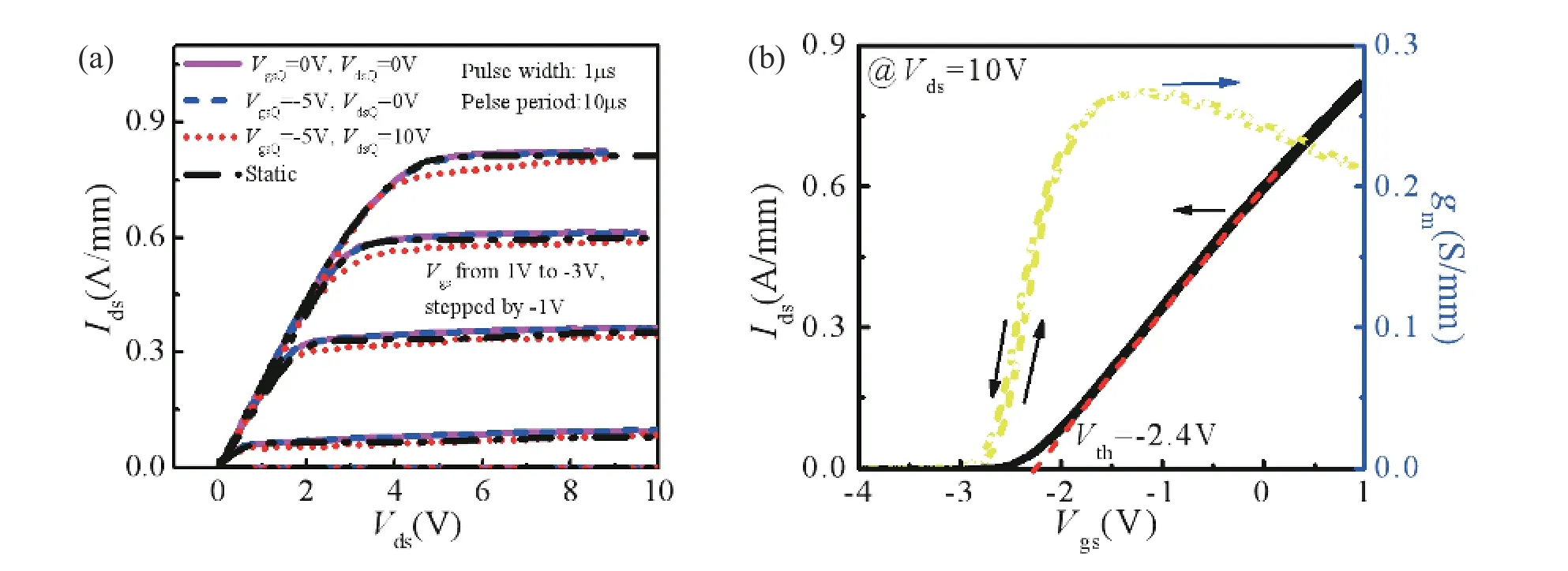
Fig.2.(Color online) (a) Static and pulsed current-voltage curves.(b) Double transfer characteristics of the AlGaN/GaN HEMTs on a GaN substrate.
The new heterostructure was grown on a GaN substrate with metal-organic chemical vapor deposition (MOCVD).The heterostructure from top to bottom was a 2-nm GaN, a 18-nm Al0.25Ga0.75N, a 1-nm AlN, a 500-nm GaN channel layer, a 1.5-μm Fe-doping GaN, and a 500-nm Mg-doping GaN, as shown in Fig.1(a).The 2DEG density and mobility were 1.0 ×1013cm-2and 1950 cm2/(V·s), respectively.The device fabrication was commenced with mesa isolation by dry etching.The metal for source/drain was Ti/Al/Ni/Au multi-layer metal,which was fabricated by electron-beam evaporation.However, realizing low ohmic resistance of Al0.25GaN/GaN heterostructures on the GaN substrate is much harder than heterostructures on other substrates, because of the lower threading dislocation densities[9].Therefore, a low-power inductively coupled plasma (ICP) etching process at source/drain regions was undertaken before ohmic metal evaporation[28,29].The radio frequency (RF) generator power, inductively coupled plasma generator power and etching time were set to 10 W, 180 W, and 1 min, separately.A ohmic resistance of 0.8 Ω·mm was realized after being annealed at 860 °C in nitrogen.The surface was passivated with 200-nm silicon nitride (SiN).The SiN in-gate region was removed by the ICP dry etching process.To reduce the damage caused by the dry etching process, a high-temperature annealing process (450 °C in nitrogen for 5 min) was taken after SiN etching.An Ni/Au asymmetric Γ-shaped gate was formed by electron-beam lithography, which is closer to the source contact.The width and lengths of the single gate is 75μm and 500 nm, respectively.The gate field plate was 650 nm, as shown in Fig.1(b).The distances from gate to source and from gate to drain were 1.08 and 2.92μm, respectively.
3.Results and discussion
The output characteristics of the AlGaN/GaN HEMTs on the GaN substrate is illustrated in Fig.2(a).The total current collapse is around 4.3%, and the gate lag is around 0.1%.The maximum drain current is 816 mA/mm, and the maximum transconductance is 264 mS/mm.In addition, the surface state is well suppressed, as reflected where the maximum deviation of transconductance is only 0.8%.
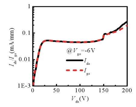
Fig.3.(Color online) 3-terminal breakdown characteristic of the AlGaN/GaN HEMT on a freestanding GaN substrate.
The 3-terminal breakdown characteristic of the AlGaN/GaN HEMT on the GaN substrate is displayed in Fig.3.The judgment basis for BV is that the drain leakage current rises to 1 mA/mm[30,31].Benefiting from the low threading dislocation densities, the homogeneous epitaxial AlGaN/GaN HEMT on the GaN substrate can achieve high BV[13,32].To realize these advantages, the asymmetric gate (larger distance of gate-drain) and the gate field plate are introduced.High breakdown voltages exceeding 200 V (200 V is the limit to our test system) have been realized in the fabricated devices(Fig.3).
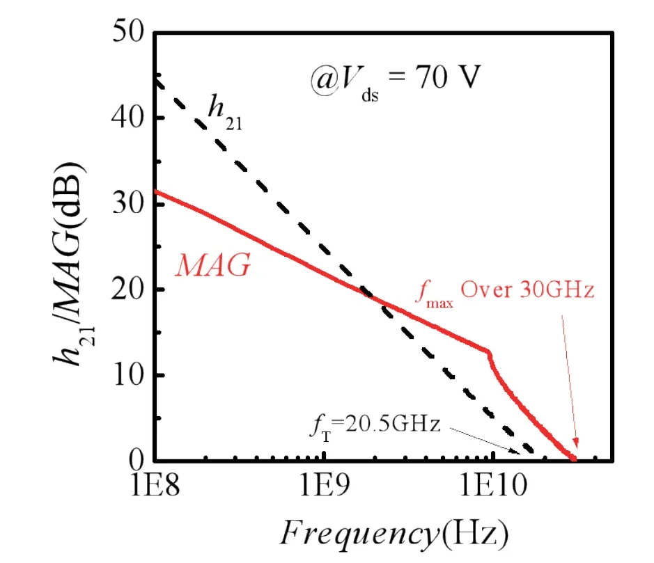
Fig.4.(Color online) Small-signal radio frequency performance of the AlGaN/GaN HEMT on a GaN substrate.
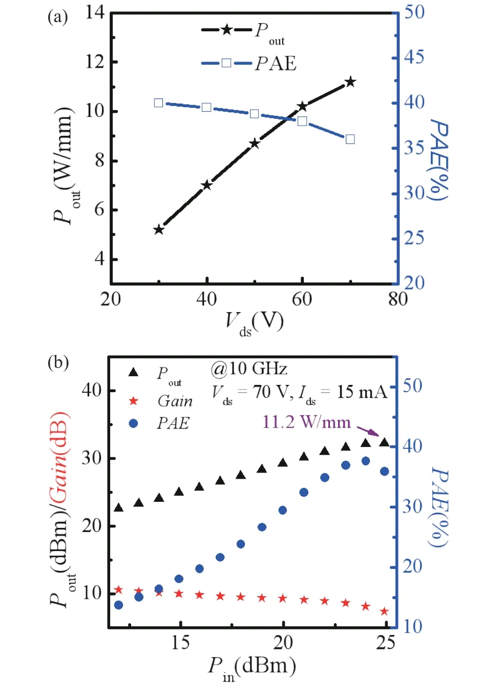
Fig.5.(Color online) Large-signal performance of the AlGaN/GaN HEMTs on a GaN substrate.(a) The CW output power and PAE vs.Vds.(b) The large-signal performance and PAE vs.Pin.
Fig.4 is the radio frequency small-signal characteristics of the fabricated AlGaN/GaN HEMT.The frequency was varied from 100 MHz to 30 GHz in 50-MHz increments during on-wafer measurements.Thefmaxof 20.5 GHz andfmaxover 30 GHz are realized, as shown in Fig.4.
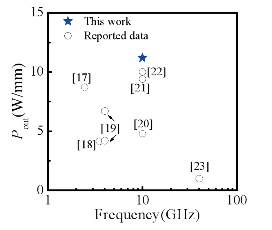
Fig.6.(Color online) Plot of Pout vs.frequency for our devices against reported AlGaN/GaN HEMT on a GaN substrate from reported results[17-22].
The continuous-wave (CW) power was measured by the load–pull system.The gate width of the measured device is 2 × 75μm.The device was operated in Class AB mode,while the drain bias was biased at 30, 40, 50, 60, and 70 V.The CW output power was increased from 5.2 to 11.2 W/mm,with the drain bias increasing from 30 to 70 V, as illustrated in Fig.5(a).The large-signal performance with drain based of 70 V was shown in Fig.5(b).The CW output power peak was 11.2 W/mm, while the power-added efficiencies (PAE) is just 36%.The value of PAE is a bit low, which can be improved by reducing contact resistance and gate length.
Many balls would start in the late evening and last until the early morning hours. Cinderella s need to leave at midnight would be an early departure from most balls.Return to place in story.
[6]Hsu J W P, Manfra M J, Molnar R J, et al.Direct imaging of reversebias leakage through pure screw dislocations in GaN films grown by molecular beam epitaxy on GaN templates.Appl Phys Lett,2002, 81, 79
4.Conclusion
In summary, X-band AlGaN/GaN HEMT on a GaN substrate with high power density has been investigated.The BV over 200 V is realized by introducing the asymmetric gate and gate field plate.The working voltage of the drain electrode is increased to 70 V during the microwave output power measured.A continuous-wave power density reaches a record value of 11.2 W/mm@ 10 GHz.However, the PAE is as low as 36%, which may be caused by large ohmic resistance and gate length.The techniques of Si ion implantation in the source/drain regions and use of a small gate will be introduced to solve this problem, improving PAE and microwave output power.Moreover, the measuredfmax/ftof our fabricated device exceeds 30 GHz/20 GHz.The results of our fabricated device demonstrate the potential of AlGaN/GaN HEMT on a GaN substrate for microwave power applications.
References
The output power densities of our device and other similar reported devices are benchmarked (Fig.6).The output power density of 11.2 W/mm for our device represents a record value among all reported references.
My sisters and I delighted in picking out little outfits5 for her and choosing pajamas6 that had to be warm because, as my sister pointed4 out, They probably don t have heat.
[5]Koehler A D, Anderson T J, Hite J K, et al.Degradation mechanisms of AlGaN/GaN HEMTs on sapphire, Si, and SiC substrates under Proton.2014 IEEE Workshop on Wide Bandgap Power Devices and Applications, 2014, 33
[3]Yue Y Z, Hu Z Y, Guo J, et al.Ultrascaled InAlN/GaN high electron mobility transistors with cutoff frequency of 400 GHz.Jpn J Appl Phys, 2013, 52, 08JN14
If only I had a duchy! What! He wants to marry me? said the scissors, and she was so angry that she gave the collar a sharp snip9, so that it had to be cast aside as good for nothing
[4]Palacios T, Chakraborty A, Rajan S, et al.High-power AlGaN/GaN HEMTs for ka-band applications.IEEE Electron Device Lett, 2005,26, 781
[1]Wu Y F, Moore M, Saxler A, et al.40-W/mm double field-plated GaN HEMTs.2006 64th Device Research Conference, 2006, 151
[2]Tilak V, Green B, Kaper V, et al.Influence of barrier thickness on the high-power performance of AlGaN/GaN HEMTs.IEEE Electron Device Lett, 2001, 22, 504
Before long the sexton25 came by and saw his master, the parson, running behind three girls. He was astonished at this and called out, Hi, your reverence8, whither away so quickly? do not forget that we have a christening to-day! and running after him he took him by the sleeve, but was also held fast to it.
[7]Hsu C Y, Lan W H, Wu Y S.Effect of thermal annealing of Ni/Au ohmic contact on the leakage current of GaN based light emitting diodes.Appl Phys Lett, 2003, 83, 2447
[9]Anderson T J, Tadjer M J, Hite J K, et al.Effect of reduced extended defect density in MOCVD grown AlGaN/GaN HEMTs on native GaN substrates.IEEE Electron Device Lett, 2015, 37, 28
[8]Nakamura S.III-V nitride-based blue LDs with modulation-doped strained-layer superlattices.Compound Semiconductors 1997.Proceedings of the IEEE Twenty-Fourth International Symposium on Compound Semiconductors, 2002, 1
My son, go and lift your father s arm up on the bench, said the queen to one of the princes, for she easily knew the king again, although she was afraid to make herself known to him
[10]Liu J P, Ryou J H, Yoo D, et al.III-nitride heterostructure field-effect transistors grown on semi-insulating GaN substrate without regrowth interface charge.Appl Phys Lett, 2008, 92, 133513
[11]Wu M, Leach J H, Ni X, et al.InAlN/GaN heterostructure field-effect transistors on Fe-doped semi-insulating GaN substrates.J Vac Sci Technol B Nanotechnol Microelectron Mater Process Meas Phenom, 2010, 28, 908
[12]Jana D, Chatterjee A, Sharma T K.Confirmation of the compensation of unintentional donors in AlGaN/GaN HEMT structures by Mg-doping during initial growth of GaN buffer layer.J Lumin,2020, 219, 116904
[13]Deen D A, Storm D F, Meyer D J, et al.Impact of barrier thickness on transistor performance in AlN/GaN high electron mobility transistors grown on free-standing GaN substrates.Appl Phys Lett, 2014, 105, 093503
You will not go to sea again, Jurgen, I suppose, observed one ofthe old fishermen. You will always stay with us now. But this was not Jurgen s intention; he wanted to see something ofthe world. The eel-breeder of Fjaltring had an uncle at Old Skjagen,who was a fisherman, but also a prosperous merchant with ships upon the sea; he was said to be a good old man, and it would not be a bad thing to enter his service. Old Skjagen lies in the extreme north of Jutland, as far away from the Hunsby dunes as one can travel in that country; and this is just what pleased Jurgen, for he did not wantto remain till the wedding of Martin and Else, which would takeplace in a week or two.
[14]Kaun S W, Wong M H, Lu J, et al.Reduction of carbon proximity effects by including AlGaN back barriers in HEMTs on free-standing GaN.Electron Lett, 2013, 49, 893
Then she told about a wise old woman in that country, who had helped many in troubles of the same kind, and could no doubt help the queen as well, if she would send for her
[15]Tanabe S, Watanabe N, Matsuzaki H.Breakdown mechanism in AlGaN/GaN high-electron mobility transistor structure on freestanding n-type GaN substrate.Jpn J Appl Phys, 2016, 55, 05FK01
[16]Zhu M D, Song B, Hu Z Y, et al.Comparing buffer leakage in Polar-MOSH on SiC and free-standing GaN substrates.2016 Lester Eastman Conference (LEC), 2016, 27
[17]Kumazaki Y, Ohki T, Kotani J, et al.Over 80% power-added-efficiency GaN high-electron-mobility transistors on free-standing GaN substrates.Appl Phys Express, 2021, 14, 016502
But they would do nothing of the sort, and, because she was not as doleful as themselves, they declared that this miserable9 life was all she was fit for
Only say good-by to all your brothers and sisters the night before you come away, and when you have gone to bed turn this ring round upon your finger and say firmly: `I wish to go back to my palace and see my Beast again
[18]Góralczyk M, Gryglewski D.S-band GaN PolHEMT power amplifier.2016 21st International Conference on Microwave, Radar and Wireless Communications (MIKON), 2016, 1
[19]Storm D F, Katzer D S, Roussos J A, et al.AlGaN/GaN HEMTs on free-standing GaN substrates: MBE growth and microwave characterization.J Cryst Growth, 2007, 301/302, 429
[20]Chu K K, Chao P C, Pizzella M T, et al.9.4-W/mm power density Al-GaN–GaN HEMTs on free-standing GaN substrates.IEEE Electron Device Lett, 2004, 25, 596
[21]Chu K K, Chao P C, Windyka J A.Stable high power GaN-on-GaN hemt.Int J Hi Spe Ele Syst, 2004, 14, 738
[22]Meyer D J, Deen D A, Storm D F, et al.High electron velocity submicrometer AlN/GaN MOS-HEMTs on freestanding GaN substrates.IEEE Electron Device Lett, 2013, 34, 199
[23]Wojtasiak W, Góralczyk M, Gryglewski D, et al.Micromachines,2018, 9, 546
[24]Asif Khan M, Yang J W, Knap W, et al.GaN–AlGaN heterostructure field-effect transistors over bulk GaN substrates.Appl Phys Lett, 2000, 76, 3807
[25]Zhang Z R, Fang Y L, Yin J Y, et al.Highmobility AlGaN/GaN high electronic mobility transistors on GaN homo-substrates.Acta Phys Sin, 2018, 67, 076801
[26]Ma T, Hao Y, Chen C, et al.A new small-signal model for asymmetrical AlGaN/GaN HEMTs.J Semicond, 2010, 31, 064002
[27]Kumar V, Chen G, Guo S P, et al.Field-plated 0.25-μm gate-length AlGaN/GaN HEMTs with varying field-plate length.IEEE Trans Electron Devices, 2006, 53, 1477
[28]Buttari D, Chini A, Meneghesso G, et al.Systematic characterization of Cl2reactive ion etching for improved ohmics in AlGaN/GaN HEMTs.IEEE Electron Device Lett, 2002, 23, 76
[29]Wang C, Cho S J, Kim N Y.Optimization of ohmic contact metallization process for AlGaN/GaN high electron mobility transistor.Trans Electr Electron Mater, 2013, 14, 32
[30]Bahat-Treidel E, Hilt O, Brunner F, et al.AlGaN/GaN/AlGaN DHHEMTs breakdown voltage enhancement using multiple grating field plates (MGFPs).IEEE Trans Electron Devices, 2010, 57, 1208
[31]Wang C, Maharjan R K, Cho S J, et al.A novel manufacturing process of AlGaN/GaN HEMT for X-band high-power application on Si (111) substrate.2012 Asia Pacific Microwave Conference Proceedings.Kaohsiung, Taiwan, China, 2013, 484
Then the train arrived at my stop. As the doors opened, I heard the old man cluck sympathetically. My, my, he said, that is a difficult predicament indeed. Sit down here and tell me about it.
[32]Chen Y C, Sanyal I, Hu T Y, et al.The influence of superlattice structure on the dynamic buffer response of AlInN/GaN-on-Si HEMTs.IEEE Trans Nanotechnol, 2020, 19, 415
 Journal of Semiconductors2024年1期
- Journal of Semiconductors的其它文章
- Bidirectional rectifier with gate voltage control based on Bi2O2Se/WSe2 heterojunction
- 240 nm AlGaN-based deep ultraviolet micro-LEDs: size effect versus edge effect
- Anisotropic etching mechanisms of 4H-SiC: Experimental and first-principles insights
- Electrical properties and structural optimization of GaN/InGaN/GaN tunnel junctions grown by molecular beam epitaxy
- Optimized operation scheme of flash-memory-based neural network online training with ultra-high endurance
- A 24-30 GHz 8-element dual-polarized 5G FR2 phased-array transceiver IC with 20.8-dBm TX OP1dB and 4.1-dB RX NF in 65-nm CMOS