The Development of 3D Atomic Force Microscopy with Magnetically Driven-Orthogonal Cantilever Probes
Hao Zhang, Junyuan Geng, Haibo Gao, Weibin Rong, Hui Xie*
The State Key Laboratory of Robotics and Systems, Harbin Institute of Technology, Harbin 150080, China
Keywords:3D-AFM MD-OCP Critical dimensions (CDs)360° characterization 3D topography reconstruction
ARTICLEINFO This paper presents a three-dimensional(3D)-atomic force microscopy(AFM)method based on magnetically driven (MD)-orthogonal cantilever probes (OCPs), in which two independent scanners with three degrees of freedom are used to achieve the vector tracking of a sample surface with a controllable angle.A rotating stage is integrated into the compact AFM system,which helps to achieve 360°omnidirectional imaging.The specially designed MD-OCP includes a horizontal cantilever, a vertical cantilever, and a magnetic bead that can be used for the mechanical drive in a magnetic field.The vertical cantilever,which has a protruding tip,can detect deep grooves and undercut structures.The design,simulation,fabrication,and performance analysis of the MD-OCP are described first.Then,the amplitude compensation and home positioning for 360° rotation are introduced.A comparative experiment using an AFM step grating verifies the ability of the proposed method to characterize steep sidewalls and corner details,with a 3D topography reconstruction method being used to integrate the images.The effectiveness of the proposed 3D-AFM based on the MD-OCP is further confirmed by the 3D characterization of a microelectromechanical system (MEMS) device with microcomb structures.Finally, this technique is applied to determine the critical dimensions (CDs) of a microarray chip.The experimental results regarding the CD parameters show that,in comparison with 2D technology,from which it is difficult to obtain sidewall information, the proposed method can obtain CD information for 3D structures with high precision and thus has excellent potential for 3D micro–nano manufacturing inspection.
1.Introduction
Micro–nano electronic components have been widely used in metamaterials [1], aerospace [2,3], the healthcare industry [4,5],environmental energy [6,7], biotechnology [8,9], and other fields since the development of integrated circuits, and micro-elements with a three-dimensional (3D) structure have been thoroughly explored due to their high information capacity.The critical dimensions(CDs)of these 3D devices,such as line edge roughness(LER), line width (LW), LW roughness (LWR), sidewall roughness(SWR), and sidewall angle, directly affect their electrical and mechanical properties [10,11]; therefore, high-precision 3Dstructure detection technology is needed to effectively ensure ultraprecision machining quality.
Several techniques are available for performing 3D metrology,such as confocal microscopy [12] and optical interferometry [13],both of which are based on optical mechanisms and are forms of non-contact measurement, making them fast, nondestructive,and therefore widely used.However, as these techniques are limited by diffraction phenomena, the lateral resolution can only reach the sub-micron level, and it is impossible to extract more 3D topographic details from the obtained artifact images.Scanning electron microscopy (SEM) [14,15] and transmission electron microscopy [16] have high resolution and fast imaging speed, but these two methods can only detect conductive samples and need to be performed in a vacuum.Moreover, the cumbersome process of sample preparation can easily lead to material modification,and accurate height information can be difficult to obtain from the gray values of two-dimensional (2D) results.Atomic force microscopy(AFM)is a powerful tool for 3D detection because it has no special requirements for the working environment,sample preparation,or materials.Outstanding sub-nanometer measurement resolution,fast imaging, and flexible probe modification can be achieved[17–19]; most importantly, AFM is a true 3D imaging approach that uses the force feedback principle.
Thus far, a variety of improvements in 3D-AFM imaging have been researched,such as system setups,probe structures,and scanning algorithms.In 1994, Martin and Wickramasinghe [20] proposed a 2D control strategy based on a flared probe: A lowfrequency horizontal vibration was attached to the vertical vibration to modulate its amplitude,thereby allowing prediction and adaptive measurement of the sidewall slope.In 2006, the Murayama team[21]incorporated a multi-angle-scanning method into CD-AFM,in which the tip approached the sidewall statically at different angles and the specimen surface was free from friction or lateral force.In the same year,they used a tilted probe to achieve tilt-step-in mode operation without friction[22].In 2015,Xie et al.[23]reported an AFM caliper that used dual optical fiber probes and could serially scan adjacent or opposite sidewalls without specimen rotation.Although 3D-AFM imaging technology has gone through decades of development, limitations remain, including complex operations[23,24],tip wear[25,26],and tip geometry convolution effects[27].
Here, we present a novel 3D-AFM imaging method based on magnetically driven (MD)-orthogonal cantilever probes (OCPs).An MD-OCP consists of a horizontal cantilever,a vertical cantilever,and a magnetic bead,where the extended vertical cantilever with a protruding tip can detect deep grooves with height h and undercut structures with an angle of α.Compared with a flared probe, the MD-OCP has the advantages of high imaging resolution and small tip geometric convolution errors.Large lateral tip rigidity helps to avoid brittle tip fracture.The proposed method does not require complex rotation coordinate transformation, as in tilt modulation,and the MD-OCP can be easily integrated into commercial systems.This method can perform 360° omnidirectional 3D imaging, benefiting from a rotating sample stage along the z-axis that is integrated into the AFM system and from 3D image-reconstruction technology to recreate the detected 3D topography.The MD-OCP works at its first-order bending resonance frequency using a magnetic force drive, which has low hysteresis, high imaging resolution, low drive quality, and fast scanning speed [28,29].In addition,the MD probe overcomes the limitations of the traditional piezo-drive method [30,31], making it more suitable for the characterization of liquid samples and the drive of probes with complex architectures, resulting in good scalability.Two independent scanners cooperate to complete the tilt vector compensation in which the vector angle β is controllable (0°–90°).The proposed method is an important supplement in the field of 3D-AFM technology and holds strong potential for 3D micro–nano manufacturing inspection.
This paper is organized as follows:Section 2 introduces the system configuration, the MD-OCP, and the performance measurement and analysis, including the performance calibration and amplitude compensation of the MD-OCP and home positioning for the 360° rotation; the experimental results and discussion are described in Section 3; Section 4 provides the conclusion.
2.Experiments
2.1.System configuration

Fig.1.Schematic of the 3D-AFM with the MD-OCP.LIA: lock-in amplifier;Osc: oscillator; RT: rotatable stage; PSD: position-sensitive detector; τ: torque;m: magnetic moment of the magnetic bead; B: magnetic flux density; Un, Ul:detection of the bending and torsional deformation of the probe, respectively;Um(ω): drive signals of the solenoid and ω is resonance frequency.[xp, yp, zp]:coordinate of the probe; [xs, ys, zs]: coordinate of the sample; h: height of the sample;α: angle of inclination of sample sidewall; β: vector angle of the probe.
Fig.1 provides a system schematic of the proposed 3D-AFM with MD-OCP.Two nano-positioning scanners are used for the sub-nanometer positioning of the sample and the probe (Scanner I: PDQ375HS; Scanner II: HS3; Mad City Labs, Inc., USA).A rotatable stage(RT)(ECR3030,Attocube Inc.,Germany)fixed on Scanner I and combined with an optical microscope realizes the rotational and coarse positioning of the sample.Sinusoidal voltage signals are supplied to the coil mounted in the sample stage, generating an electromagnetic field along the vertical direction in space.In this way, the magnetic bead attached to the probe is subjected to a torque: τ = m × B (where m is the magnetic moment of the magnetic bead and B is the magnetic flux density), which is used to mechanically oscillate the probe at its first-order bending resonance frequency[31,32].Compared with triangular wave signals,a sinusoidal voltage drive can effectively reduce the mechanical vibration caused by a sudden change at the corner of a triangular wave, thereby improving the scan speed [33,34].Deformation of the cantilever is detected via an optical lever containing a laser and a position-sensitive detector (PSD), which includes detection of the bending (Un) and torsional (Ul) deformation of the probe.A specialized AFM probe-dynamics controller (Dual-OC4, Nanonis GmbH, Germany) with an oscillator (Osc) and lock-in amplifier(LIA) is used to process the feedback signal of the probe.During scanning,the probe tracks the sample surface with a motion vector on the yz-plane using a controllable vector angle β.In the experiments, the mechanical amplitude and frequency were set at 50 nm (70% of the free oscillation amplitude) and 47.574 kHz,respectively.
2.2.Magnetically driven-orthogonal cantilever probe
2.2.1.Design and analysis
Fig.2 provides the scheme of the proposed MD-OCP, which is composed of a horizontal cantilever, a vertical cantilever with a protruding tip, and a magnetic bead (made from a ferromagnetic material).The magnetic bead, which is bonded in the corner, is magnetized along the longitudinal axis of the horizontal cantilever.The horizontal cantilever and vertical cantilever are distributed orthogonally, further extending the detectable range in the vertical.The protruding tip not only is conveniently visible from the top view but also has the ability to scan re-entrant structures.The interaction between the MD-OCP and the sample is reflected in the deflection/torsion of the horizontal cantilever.
According to the Euler–Bernoulli beam theory, when the materials of the horizontal cantilever and vertical cantilever are the same(Young’s modulus;E;Poisson’s ratio:ν),the bending stiffness(kb) and torsional stiffness(kt) of the MD-OCP can be expressed as follows [35]:

Fig.2.Schematic of the MD-OCP.L, W, T: length, width, and thickness of the horizontal cantilever, respectively; l, w, t: length, width, and thickness of the vertical cantilever, respectively; d: diameter of magnetic bead.
where L,W,and T are the length,width,and thickness,respectively,of the horizontal cantilever; and l, w, and t are the length, width,and thickness, respectively, of the vertical cantilever (Fig.2).

2.2.2.Fabrication
First,the MD-OCP’s horizontal cantilever and vertical cantilever with a protruding tip were separately prepared by means of the focused ion beam(FIB)milling(FIB/SEM dual beam system,Helios NanoLab 600i, FEI Company, USA) of two commercial probes (HQ:NSC18/Al-BS, MikroMasch, USA; and ATEC-FM, Nanosensors,Switzerland).A ferromagnetic bead with a diameter similar to the width of the horizontal cantilever was then bonded to the free end of the horizontal cantilever using an epoxy adhesive(A-05HP,Angeluo, China).Finally, the vertical and horizontal cantilevers were assembled and glued as designed.The detailed equipment and assembly process is provided in our previous studies [35,36].Fig.5 shows SEM images of the prepared MD-OCP, with the geometric parameters marked.
The batch fabrication of the probe involves two main approaches: ①The orthogonal cantilever is prepared by 3D printing technology, while the fabrication of the tip and bead relies on micromanipulation technology.②The cantilever and the tip are prepared by means of chemical etching and growth, and the bead is assembled manually.Thus,the probe fabrication is similar to the preparation of a cantilevered micropipette probe in that it is a combination of human effort and machine work.Improvement of this detailed process requires further research by professionals.
2.3.Performance measurement and analysis
2.3.1.Performance calibration of the MD-OCP
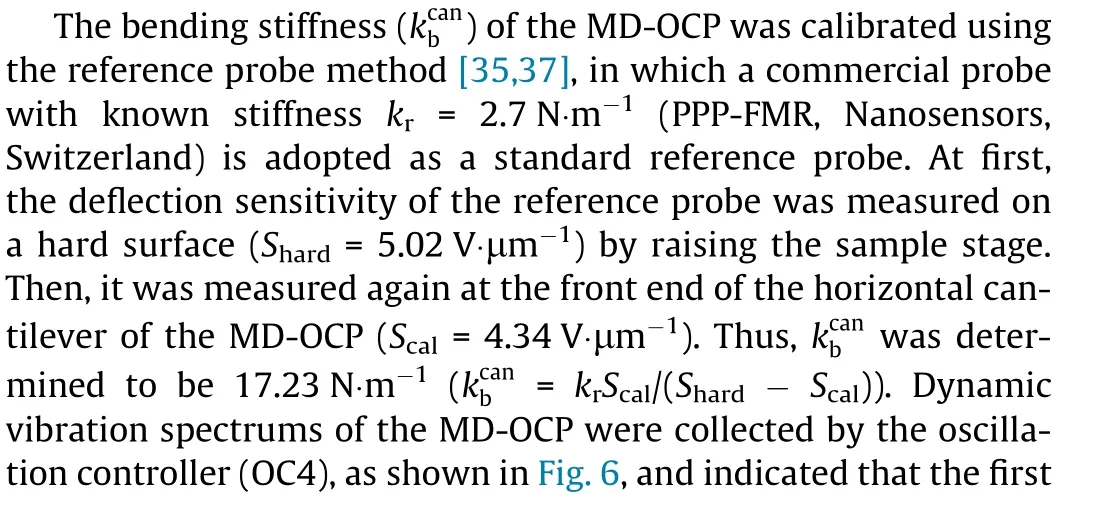

Fig.3.Variations in the stiffness and the first resonance frequency with different (a) vertical cantilever lengths and (b) horizontal cantilever lengths.

Fig.4.FEA dynamic analysis of the MD-OCP.

Fig.5.SEM images of the MD-OCP: top view and side view (inset).
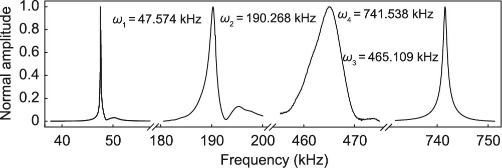
Fig.6.Dynamic vibration spectrums of the MD-OCP.

In the experiment, the first resonance frequency (ω1) of the MD-OCP was used, which can cause crosstalk from higher order modes.Fig.7 shows the amplitude response of the MD-OCP at different frequencies under mechanical excitation at ω1.It can be concluded from the experimental results in Fig.7(a)and the simulation results in Fig.7(b)that the high-order amplitude response is very low and insufficient to cause crosstalk.In addition, it can be seen that the MD-OCP has a twist at the working frequency,which means that the MD-OCP is actually vibrating in an oblique direction, caused by its own structural characteristics.
2.3.2.Amplitude compensation of the MD-OCP on the y-axis
As shown in Fig.1, during 3D imaging, Scanner I is responsible for the raster scanning on the xy-plane.The y-axis of Scanner II and the z-axis of Scanner I cooperate to realize the oblique compensation in the yz-plane.The relative movement of the MD-OCP laser spot along the y-axis will cause the amplitude of the probe to change.As shown in Fig.8, when the offset value reached 5 μm along the y-axis, the amplitude of the output voltage dropped by 2.2%–5.8% (red dotted line).Therefore, amplitude compensation of the MD-OCP is necessary and can be calculated as follows:

2.3.3.Home positioning for 360° rotation
In practice,it is almost impossible for the target sample to coincide with its center of rotation, meaning that the target sample deviates from its original position after rotation.Therefore, it is necessary to compensate for this eccentricity during 360°imaging.In this paper, a home positioning method is used to automatically compensate for the off-center displacement(Δx and Δy).As shown in Fig.9(a),prior to the experiment,the coordinates of the center of the target sample Otswere obtained by processing the optical image obtained from the top view (xy-plane) (Fig.9(a-i)), which includes gray processing (Fig.9(a-ii)), thresholding (Fig.9(a-iii)),hole filling (Fig.9(a-iv)), and edge contour extraction and center point positioning(Fig.9(a-v)).It should be noted that the upper left corner of the optical image was chosen as the coordinate origin O(0, 0), as shown in Fig.9(b), and the distance corresponding to a unit pixel of the optical image is 0.33 μm [36].During calibration of the rotation center Oc,the sample was rotated counterclockwise num times(num=3–5)with a certain angle θr(e.g.,θr=2°),and the center coordinates of the target sample were recorded as (x0, y0),(x1, y1),..., (xnum, ynum).Then, the rotation center and rotation radius of the target sample Oc(xc, yc) and R were obtained by the least-squares method.As shown in Fig.9(c), the eccentricity compensation for θrrotation can therefore be given by the following:

Fig.7.Amplitude response of the MD-OCP at different frequencies under the mechanical excitation at ω1.(a) Experiment; (b) simulation.
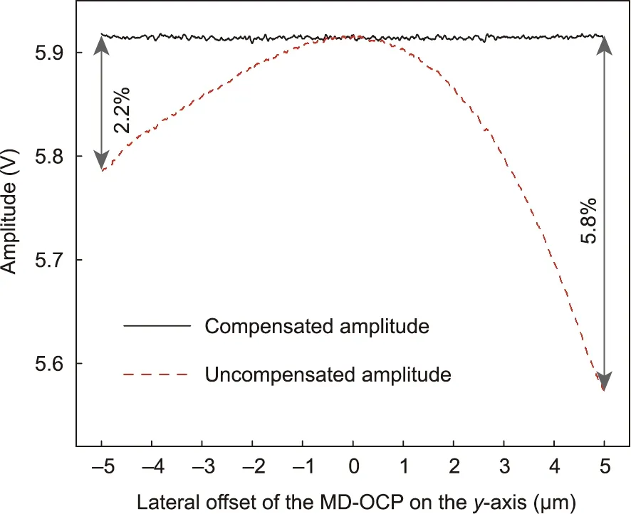
Fig.8.Amplitude compensation when the MD-OCP moves along the y-axis.

Fig.9.Positioning method: (a) image processing; (b) calibration of the rotation center of the target sample; (c) compensation displacement calculation.Ots:coordinates of the center of the target sample;Oc:rotation center;R:rotation radius of the target sample;A–E:the center of the target sample after each rotation;P0,P1:points; θ0: the initial angle; θr: certain angle.
where θ0is the initial angle of point P0—that is, the angle between OcP0and the y-axis.
Points A–E shown in Fig.9(b) represent the center of the target sample after each rotation, the coordinates of which are (69.96,288.75), (151.47, 259.05), (220.44, 232.32), (293.70, 201.30), and(359.37, 170.28) (unit: μm), respectively.Based on this, the rotation center Ocis (-759.32, -2157.23) (unit: μm) and the rotation radius is R = 2582.58 μm.Thus, if point A is the starting point and the rotation angle θris 90°, then Δx = 1616.52 μm,Δy = -3275.10 μm, and θ0= 18.73°.
3.Results and discussion
3.1.Characterization of the AFM step grating
In this part of the research,an AFM step grating with a nominal height of (560.0 ± 2.6) nm (TGZ3, NT-MDT, Russia) was measured using two methods (the traditional tapping mode and the proposed method) to determine the 3D imaging performance of the proposed method for steep sidewalls and corner details.The traditional tapping mode(Dimension Icon,Bruker Co.,USA)uses β=45°and a standard probe k = 3 N·m-1(RFESPA-75, Bruker Co., USA),front angle (15 ± 2)°, back angle (25 ± 2)°, and side angle (17.5 ±2.0)°.Figs.10(a)and(b)provide SEM images of the AFM step grating,from which it can be seen that the width of the grating is about 1.16 μm and the height is about 563.2 nm ((443.8/sin52°) nm).
Figs.10(c)and(d)provide the characterization results obtained by using the standard probe in the traditional tapping mode.During imaging,400 lines were scanned and 400 points were detected on each scan line.The scan rate was chosen to be 50 Hz.The difference between these two mapping results is mainly caused by the relative position of the probe and the sample.As shown in Fig.10(c),when the cantilever is parallel to the grating,the characterization result is mainly affected by the side angle of the tip.Therefore,the inclination angles on both sides of the obtained grating are basically the same (Fig.10(e)), and the critical angle that the standard probe can scan is 72.5°.However,when the cantilever is perpendicular to the grating (Fig.10(d)), the characterization result is related not only to the front and back angle of the tip but also to the installation angle of the probe 13°.As shown in Fig.10(f), the measured angle difference between the two sidewalls is 18.4°, while the theoretical difference is 16° ((15° + 13°)- (25° - 13°)).It should be noted that the above analysis ignores the installation angle of the sample, and the inclination angle is obtained by the linear fitting of the part corresponding to the dotted line in the figure.As mentioned above, due to the influence of the tip shape,the traditional tapping mode using a standard probe cannot obtain the sidewall information of the grating and can only be used to analyze the height of the sample.The measured height(Hsp) results are shown in Table 1.
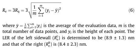
Fig.10(g) shows two sets of 3D scanning point clouds at opposite locations obtained by the proposed method, and the reconstructed 3D image is presented below it.The 3D scanning point clouds consist of 290 scan lines and 176 points on each scan line.The imaging speed was set as 50 Hz.Figs.10(h)–(k)show the profiles at the line marked in Fig.10(g), and the corresponding CD parameters are given in Table 1.Fig.10(h) gives three crosssections of the grating in the yz-plane and shows that the step height (H) of the TGZ3 obtained by the MD-OCP is (562.9 ± 1.6)nm, which is consistent with the result of the standard probe.In addition, the cross-sections show that the inclination angle on the left side is (82.54 ± 0.27)°, while that on the right side is(81.77 ± 1.03)°; the inclination angles are related to the manufacturing process.The LW in Fig.10(h) shows that the grating gradually narrows from the bottom (1.38 μm) to the top (1.05 μm),which corresponds to the inclination angle of the sidewall.To measure the LWR of the grating,245 cross-sections were taken at each height,as shown in the inset in Fig.10(i).The LWR(Rw)can then be calculated with the following [23]:
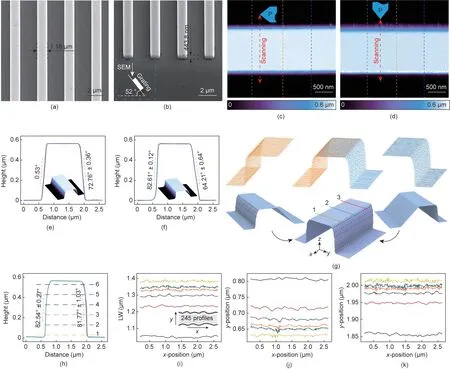
Fig.10.SEM images of the AFM step grating in(a)top view and(b)52°tilting view.Characterization results obtained by using the standard probe in the traditional tapping mode.(c)The cantilever is parallel to the grating.(d)The cantilever is perpendicular to the grating.(e,f)Profiles of the lines marked in(c)and(d),where the inset is the 3D imaging.(g)3D imaging results obtained by the proposed method.Point cloud data and 3D stitched image results,x–y range:2.9 μm×2.7 μm.Profiles of the lines marked in(g).(h) Cross-sections.(i) LW, LER of the (j) left and (k) right sidewall.

Table 1CD results of the AFM step grating.
3.2.Characterization of the micro-electromechanical system (MEMS)device
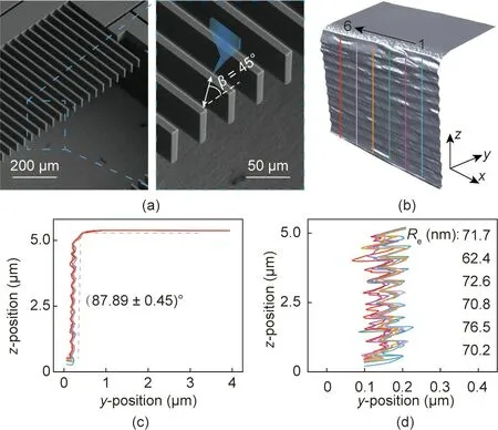
Fig.11.(a) SEM images of the MEMS device (left) and the enlarged view (right);(b) 3D imaging result of the MEMS device, x–y range: 6.3 μm × 4.0 μm;(c, d) profiles of the topography extracted from (b).
To further verify the ability of the proposed method based on the MD-OCP to perform 3D imaging in steep sidewalls, an MEMS device with microcomb structures fabricated by means of deep reactive ion etching was studied.Fig.11(a)shows the SEM images of the microcomb structure, which is composed of uniform teeth.Before scanning,the MD-OCP first made contact with the top of the target microcomb; the sample then retreated a distance along the z-axis and the fast-scan axis(y-axis)in turn.While ensuring the tip was located over the gap between two teeth,the sample was raised along the z-axis to a certain height.During 3D scanning, the scan speed was chosen to be 50 Hz, and the MD-OCP approached obliquely to the sidewall at an inclination angle β of 45°, as shown in the enlarged view in Fig.11(a).The 3D imaging results from the MEMS device, in which the number of scan lines and the points collected on each scan line were set at 788 and 500, respectively,are provided in Fig.11(b).Fig.11(c) describes the corresponding height profiles of the six lines marked in Fig.11(b).From the linear fitting results of these six curves,the inclination angle of the MEMS sidewall can be obtained and is found to be about 88°.Fig.11(d)provides an enlarged view of the profiles of the sidewall, from which the LER of the sidewall can be obtained.The mean of the LER calculated from the six profiles shown in Fig.11(d) is(70.8 ± 4.8)nm.
3.3.Characterization of the microarray chip
The above experimental results show that,compared with standard probes,the proposed method based on the MD-OCP can obtain more detailed CD parameters of the 3D structure and has excellent characterization capabilities for vertical sidewalls.This subsection describes the 360°imaging of a microarray chip unit combined with the proposed method in which β = 45°, and compares it with the characterization results of a commercial standard probe (RFESPA-75, Bruker Co., USA).The microarray chip is a type of biochip and is a support for carrying the detector with biological information at a high density, such as nucleic acids [39,40], proteins [41,42],and biological tissues [43,44].Interaction between the detector and the target molecule in a sample yields biological information,which is the main function of the biochip.Due to their highly specific surface,microarray chips have been extensively studied[45].The CD parameters of a microarray chip unit can cause differences in chip quality by affecting the adhesion and distributed density of the biodetector on the substrate.It is therefore critical to evaluate the CD parameters of microarrays using 3D measurement technology.
The microarray chip studied in this part of the research was fabricated on a polymer(intermediate polymer stamp(IPS))substrate using nanoimprinting technology[46].As shown in Figs.12(a)and(b),the characterized microarray unit is a square with a side length of about 15.5 μm and a height of about 2 μm.In addition,it can be seen from Fig.12(b)that the edges of the microarray unit are irregular and that many fish-scale-shaped burrs are distributed on the sidewall,especially within 1.5 μm in height(see the enlargement);these are the residual materials that collect during the nanoimprinting process and are piled up at the bottom.However, SEM images primarily allow qualitative analysis and are difficult to use to achieve quantitative description.Therefore,it is very necessary to perform the 3D AFM high-precision characterization of CD parameters.Fig.12(c) shows the results of 3D imaging of the microarray unit from different angles: 0° (A), 90° (B), 180° (C),and 270°(D)(A–D:sidewall).Each section contains 516 scan lines and 258 sampled points per line,which were obtained with a scan rate of 50 Hz.The 3D images of the sidewalls show the same characteristics as the SEM images.It can be seen from Fig.12(d),where the connected feature points are marked with circles of the same color for comparison, that the 3D morphological reconstruction is highly consistent with the SEM image.

Fig.12.SEM images of the microarray unit in(a)top view(characterized)and(b)side view.Note that these microarray units are from the same batch but are not identical,and(a)is the sample being studied.(c)Topography sequence acquired at rotation angles of 0°(A),90°(B),180°(C),and 270°(D)(A–D:sidewall);x–y range:10 μm×20 μm.(d) 3D reconstructions of the topography, in which the connected feature points are marked with circles of the same color.
Fig.13 gives the experimental results obtained by the two methods to characterize the microarray unit, from which its CD parameters can be analyzed.Fig.13(a) shows the sectional curves of the microarray unit at different positions, with six lines along the z-axis and four lines parallel to the xy-plane.Fig.13(b) shows the 3D imaging (left) and 2D topography (right) of the microarray unit with 516 scan lines and 516 points on each line, which was obtained by the standard probe with an imaging speed of 50 Hz.Figs.13(c)–(f) and Figs.13(g)–(j) respectively show the CD parameters obtained by the above two methods, and the corresponding CD parameters are given in Tables 2–4.As shown in Figs.13(c) and (g), the two methods give the same height for the microarray unit, which is about 2.0 μm.The measured height is slightly smaller than the height in the SEM image (Fig.12(b))because the sample is stretched during the preparation of the SEM sample.In addition, the upper edge of the sample had some bumps (~500 nm), which may be caused by a retraction of the nanoimprinting.The measured LW shows that the microarray unit is not an ideal square; its width difference is about 300–600 nm (LWAC>LWBD).However, the LW obtained by the traditional method is larger than that obtained by the proposed 3DAFM.The reason for this differenceis that the height of the sample is too high, which causes the sidewall of the tip to interact with the edge of the sample.This not only affects the height measurement but also affects the acquisition of information on the sidewall of the sample.Figs.13(d) and (h) show the profiles of the sidewall along the z-axis, from which it can be seen that there was obvious accumulation at a distance of about 1.50 μm from the bottom.Such material accumulation may be caused by the elastic recovery of some imprinted parts with elastic deformation after the pressure is unloaded.However, the sidewall angle obtained by the traditional method is significantly smaller than that obtained by the proposed method.To further analyze the angles of the sidewalls of the microarray unit obtained by the two methods, ten curves were collected on the four sidewalls for analysis; the results are shown in Table 4, where the angles in brackets are the critical angles that can be measured by the traditional method.The experimental results show that, except for the C sidewall, the sidewall angles measured by the two methods are basically the same; however, the deviation of the C sidewall is relatively large, indicating that the measurable sidewall angle of the traditional method is very limited.
Figs.13(e) and (i)provide the profiles of the sample top,which show that the surface roughness () obtained by the standard probe is smaller than that obtained by the proposed method; this is mainly caused by the difference in the profile position and the tip radius.The profiles of the D sidewall from top to bottom are shown in Figs.13(f) and (j), in which the corresponding Rqvalues are given.The experimental results show that the Rqobtained by the proposed method gradually increases from top 7.0 nm to bottom 43.5 nm, which is consistent with the SEM image.However,the same phenomenon did not appear in the results obtained by the traditional method.This is mainly because the traditional method obtains fake 3D information, and there is no y-direction information but only z-direction information.In addition, the tip of the standard probe cannot touch the nearly vertical part of the sidewall (the part above the accumulation).These experimental results show that the proposed 3D-AFM technology can quantitatively analyze the CD parameters of the tested samples and provide technical support for the optimization of nanoimprinting technology.

Fig.13.3D imaging results of the microarray unit: (a),(c–f) were obtained by the 3D-AFM based on the MD-OCP; and (b),(g–j)were obtained by traditional tapping mode based on the standard probe.(a)Sectional curves at different positions of the microarray unit,which represent the locations of the profiles in(c–f).(b)3D imaging(left)and 2D topography imaging (right) of the microarray unit, where the locations of the profiles in (g–j) are marked.(c, g) Sectional curves along the z-axis.(d, h) Profiles of the sidewall.(e, i) Surface roughness of the top.(f, j) Surface roughness of the sidewall D at different heights.Rq: surface roughness.

Table 2CD parameters of the microarray unit using the 3D-AFM based on the MD-OCP.
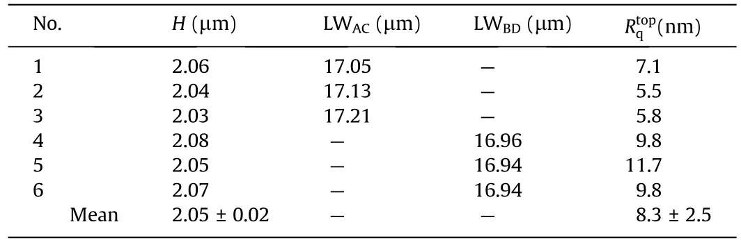
Table 3CD parameters of the microarray unit using the traditional tapping mode based on the standard probe.

Table 4Sidewall angle of the microarray unit.
4.Conclusions
This paper proposes a 3D-AFM method based on an MD-OCP,in which an in-house-built AFM system integrates a rotating stage to achieve 360°omnidirectional imaging,and two independent scanners are used to realize the vector tracking of the probe.The MDOCP was designed and optimized through simulation analysis and then prepared using a nanorobotic system.It consists of a horizontal cantilever, a vertical cantilever, and a magnetic bead that can be used for the magnetic drive.The protruding tip on the vertical cantilever allows the MD-OCP to detect deep grooves and undercut structures.In the experimental part,an AFM step grating was first used to set up a comparison experiment with the traditional method based on a standard probe;this experiment verified the ability of the proposed method to characterize steep sidewalls and corner details and revealed the limitations of the standard probe.3D reconstruction technology was used to integrate and display the results.Then,the characterization of an MEMS device with microcomb structures further proved the MD-OCP’s ability to measure vertical sidewalls.Finally, a microarray chip was studied to determine the CD parameters of a microarray unit.The experimental results demonstrated the 3D imaging capabilities of the proposed method and revealed its clear advantages over 2D imaging methods.The proposed method can achieve the quantitative analysis of the CD parameters of a sample at the nanometer scale without modifying the laser system.It is a new method to improve AFM characterization techniques and is expected to have a long-term impact on the performance characterization of microarray chips.
Acknowledgments
This work was supported in part by the National Key Research and Development Program of China (2018YFB1304903), in part by the National Natural Science Foundation of China (62003116,61925304, and 62127810), in part by the Project funded by China Postdoctoral Science Foundation (2021M690832), and in part by the Heilongjiang Postdoctoral Fund of China (LBH-Z20138).
Compliance with ethics guidelines
Hao Zhang,Junyuan Geng,Haibo Gao,Weibin Rong,and Hui Xie declare that they have no conflict of interest or financial conflicts to disclose.
- Engineering的其它文章
- Development of a High-Capacity Portable Biomass-Combustion-Powered Thermoelectric Generator
- Resolving the Adhesive Behavior of 1D Materials: A Review of Experimental Approaches
- Selective and Independent Control of Microrobots in a Magnetic Field:A Review
- Single-Molecule Methods for Characterizing Different DNA Higher-Order Structures
- Long-Term Cultivation and Meta-Omics Reveal Methylotrophic Methanogenesis in Hydrocarbon-Impacted Habitats
- Acoustic Micro-Manipulation and Its Biomedical Applications

