Rubidium-induced phase transitions among metallic,band-insulating,Mott-insulating phases in 1T-TaS2
Zhengguo Wang(王政国), Weiliang Yao(姚伟良), Yudi Wang(王宇迪), Ziming Xin(信子鸣),Tingting Han(韩婷婷), Lei Chen(陈磊), Yi Ou(欧仪), Yu Zhu(朱玉),Cong Cai(蔡淙), Yuan Li(李源), and Yan Zhang(张焱)
International Center for Quantum Materials,School of Physics,Peking University,Beijing 100871,China
Keywords: angle-resolved photoemission spectroscopy,metal-insulator transition,transition metal dichalcogenides
1.Introduction
Interactions among different degrees of freedom compete with each other in materials,resulting in an emergence of electronic phases with distinctive electronic properties.[1-6]In order to manipulate these electron phases in functional devices or to understand their underlying physics, being able to tune the interactions in materials and realize phase transitions using non-thermal experimental methods is important and becomes one of the central issues of condensed matter physics.Pressurizing and carrier doping are two commonly used methods that drive phase transitions.Pressurizing normally modulates the itineracy of electrons,[1,2,6]while carrier doping shifts the chemical potential of materials and modulates the screening of Coulomb interactions.[1-4]
The 1T-TaS2is a two-dimensional (2D) transition metal dichalcogenide that shows complex and intriguing phasetransition behaviors.[6-11]It is metallic at high temperature.Upon cooling, it undergoes successive phase transitions and enters an insulating phase with apR13.9°commensurate charge-density-wave (C-CDW) order.In the early studies, it was proposed that the low temperature insulating phase(LTIP)is a Mott insulator.[6-10]The electronic structure reconstructs in the C-CDW state forming a single half-filled band at the Fermi energy(EF).The effective in-plane hopping of electrons (t‖) is strongly suppressed due to the large unit cell of the CDW order, which allows the Mott-insulator transition to arise in the presence of a moderate on-site Coulomb interaction(U).Recently,the Mott scenario is seriously challenged by the observation of interlayer dimerization in 1TTaS2.[11-17]Considering the presence of a moderate inter-layer hopping(t⊥),dimerization of two nearest TaS2layers occurs.The unit cell consists of two electrons, suggesting that the low-energy band is full-filled and the LTIP is a band insulator.While the Mott insulating phase may not be found in bulk 1TTaS2at low temperature, a high temperature insulating phase(HTIP)was discovered recently in a small temperature region close to the C-CDW transition.[17]It was found that the interlayer dimerization vanishes in the HTIP, which makes the HTIP a promising candidate for realizing a Mott localization in 1T-TaS2.
Different degrees of freedom compete with each other in 1T-TaS2,making it an ideal system to search for phase transitions that are manipulated by non-thermal experimental methods.It was found that the insulating property of this system is unstable against various perturbations.Metal-insulator transitions (MIT) can be induced by laser pulse, current pulse,strain,gating,local electric field,pressure,chemical substitution,etc.[6,15,18-24]In this work,we succeed in driving a MIT in 1T-TaS2via rubidium surface deposition.Utilizing angleresolved photoemission spectroscopy(ARPES),we found that the rubidium-induced MIT occurs in two different ways.In the LTIP at 205 K, the rubidium deposition dopes electrons into the conduction band and drives a normal MIT via bandfilling,while in the HTIP at 225 K,when doping with a small amount of rubidium, the insulating gap collapses rapidly and meanwhile the spectral weight transfers from the high binding energy toEF, manifesting a bandwidth-controlled Mott transition.Our observation of the two distinct MITs not only confirms the existence of both Mottness and interlayer dimerization in 1T-TaS2from a carrier-doping perspective, reflecting a close competition amongt‖,t⊥, andU, but also highlights the rubidium deposition as an effective method to tune the phase transitions in 1T-TaS2.The high sensitivity of 1TTaS2to temperature and rubidium deposition can be used in searching for exotic phases and also help to design functional phase-changing devices.
2.Materials and methods
High quality single crystals of 1T-TaS2were synthesized using chemical vapor transport method.After mixing the appropriate ratio of Ta powder and S pieces(2%excess)well,the compound was sealed in a quartz tube with ICl3as the transport agent.The quartz tube was put in a two-zone furnace with thermal gradient between 750°C-850°C for 2 weeks,and then quenched in water.ARPES measurements were performed at Peking University using a DA30L analyzer and a helium discharging lamp.The photon energy was 21.2 eV.The overall energy resolution was~12 meV and the angular resolution was~0.3°.The crystals were cleavedin-situand measured in vacuum with a base pressure better than 6×10-11mbar.To measure the metallic phase of 1T-TaS2,the sample was cooled down directly from room temperature to 240 K.To measure the LTIP and HTIP,the sample was first cooled down to 80 K rapidly (~20 K per minute), and then heated up slowly (~2 K per minute) to 205 K and 225 K respectively.[17]The rubidium deposition was conductedinsituusing a rubidium dispenser.The deposition process repeated several times with a 5.6 A working current.The doping level of each doping step was represented using the total deposition time.For each doping level,the data collection duration was set to be around 10-20 min to avoid the desorption of rubidium adatoms from the sample surface at high temperature.
3.Results and discussion
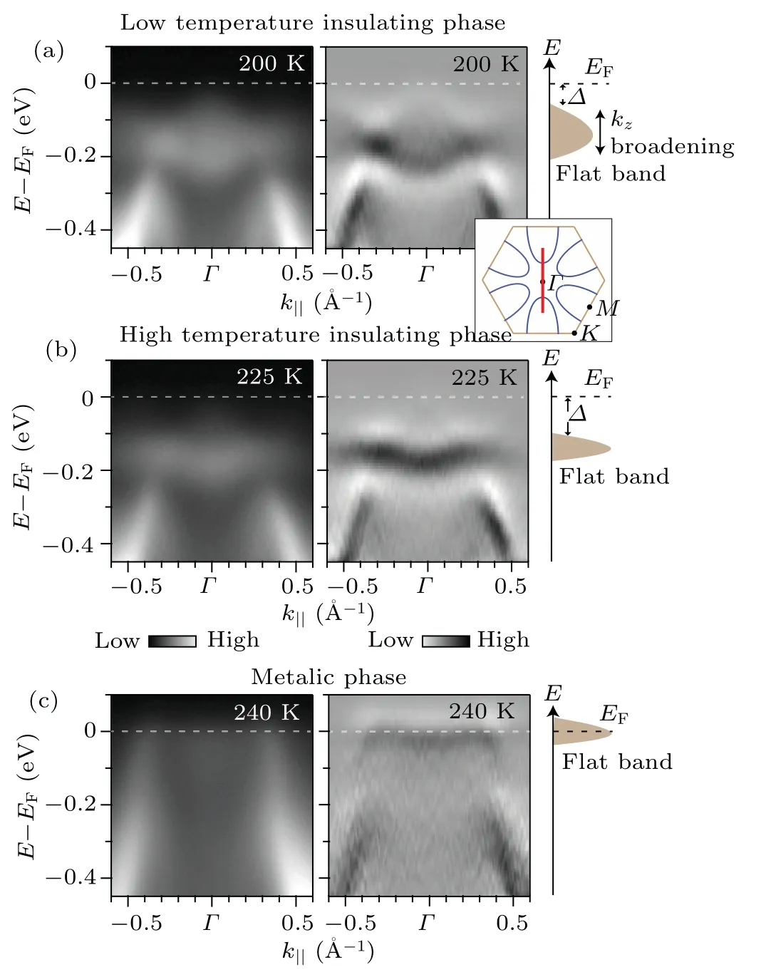
While 1T-TaS2has been well studied at both the room temperature and the liquid-helium temperature, we focus on an intermediate temperature region near the C-CDW transition where three different phases have been identified.[17]Figure 1 shows the low-energy band structure of 1T-TaS2taken at 205 K, 225 K and 240 K.At 205 K, the system is in the LTIP.The low energy electronic structure is characterized by a flat band,whose band dispersion is relatively flat along the inplane (t‖) direction.However, according to previous photonenergy dependent ARPES studies,[13,17,23,25]the out-of-plane(kz) band dispersion of the flat band is moderate.ARPES is surface sensitive, and thus sees the surface projection of the bulk electronic structure.Band dispersions from differentkzproject into one cut,resulting in a significantkz-broadening of the APRES spectra[Fig.1(a)].When the sample temperature is increased to 225 K, the system undergoes an insulator-toinsulator transition(~217 K)and enters the HTIP.[17]Thekzdispersion of the flat band is strongly suppressed as characterized by the vanishing of thekz-broadening effect [Fig.1(b)].Such a band reconstruction indicates a suppression oft⊥and was used as an evidence to support the presence of Mott localization in the HTIP.[17]When the sample temperature is increased to 240 K above the C-CDW transition(~233 K),the insulating gap is closed and the system is in the metallic phase[Fig.1(c)].

Fig.1.Characterization of the different electronic phases of 1T-TaS2.(a)Raw(left panel)and second derivative(right panel)images of the energymomentum cut taken along the Brillouin center(Γ)-Brillouin boundary(M)direction at 205 K and the corresponding schematic illustration of the density of states (DOS) of the flat band.(b) and (c) are similar to (a) but taken at 225 K and 240 K, respectively.Inset panel illustrates the Fermi surface of 1T-TaS2 (blue line)and the location of the energy-momentum cut(red line).
Figure 2 shows how different phases respond to the rubidium deposition.Note that,the influence of alkali-metal deposition has been studied previously in 1T-TaS2.[26-29]It was reported that the alkali-metal intercalation plays a dominating role and drives various CDW transitions.Here,the total rubidium coverage is estimated to be below 0.1 monolayer (ML),which is much lower in comparison to the large amount of alkali-metal used in previous studies.[26-29]Furthermore, the alkali-metal intercalation in 1T-TaS2leads to an opening of a huge gap(~500 meV)atEF.[27]Such signature of intercalation is not observed in the entire doping range in our experiments.Therefore, the alkali-metal intercalation is less relevant here.Instead, the alkali-metal adatoms could be viewed as carrier donors that donate electrons to the sample surface.In Figs.2(a)-2(c),we observe a clear rubidium-induced doping effect in the metallic state as characterized by a shifting of Fermi crossings(kFs).The Fermi surface of 1T-TaS2consists of six ellipse-like electron pockets at theMpoints.If we assume that the ellipse-like electron pockets expand uniformly with rubidium doping and calculate the Fermi surface volume according to the measuredkFs along theΓ-Mdirection,we estimate that the total doping level is~0.08 electrons per unit cell for a~90 s deposition time, which corresponds to a~0.08 ML total coverage of rubidium(see supplementary material for details).
For a normal band insulator, the doped electrons would fill into the bottom of the conduction band.As a result, the Fermi level would shift rapidly from the gap center to the conduction band bottom.This is what we observed in the LTIP[Figs.2(d)-2(f)].With the rubidium deposition,the flat bands shift to higher binding energy, indicating a chemical potential shift, and the conduction band bottom emerges atEF.In contrast to the rigid-band shift behavior observed in the LTIP,the HTIP responds to the rubidium deposition in a completely different way.It is manifested in a rapid collapsing of the insulating gap[Figs.2(g)-2(i)].When doping with a small amount of rubidium,the flat band fades away and a new band emerges atEF.Note that, aside from the flat band, all other bands are almost doping independent,which suggests that the CDW gap is little affected by rubidium in this dilute doping range.
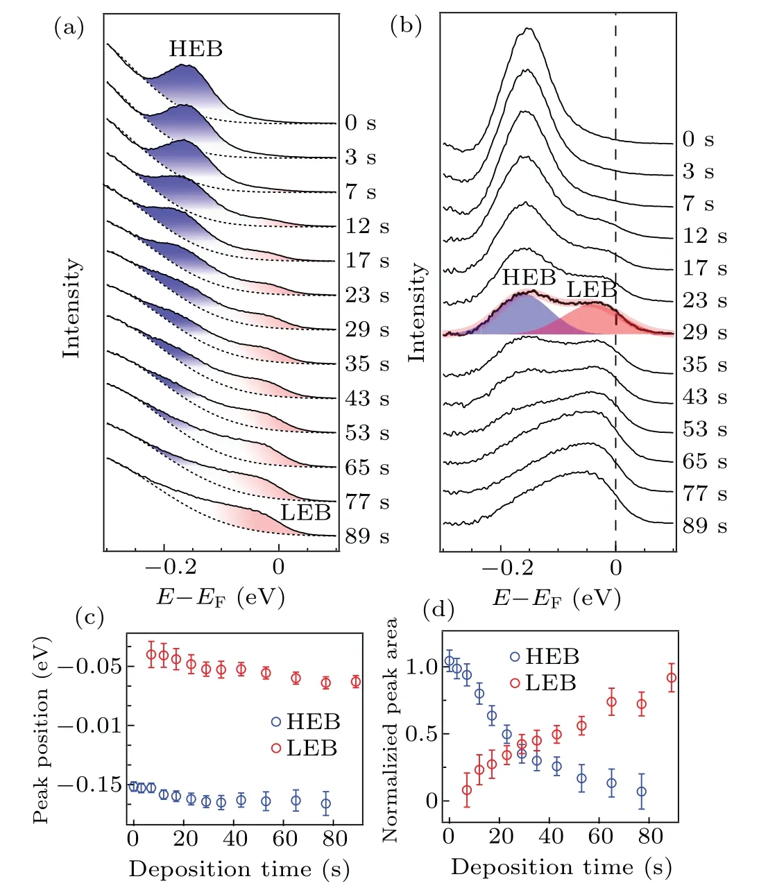
To characterize the rubidium-induced gap collapsing observed in the HTIP, Fig.3 plots the detailed doping dependence of the energy distribution curves(EDCs)taken at thekFs of the flat band.The backgrounds in Fig.3(a)originate from the tail of a broad peak at high binding energy(~-0.35 eV)[Fig.2(e)].We then fit the background using a tail of a Gaussian function.After subtracting the backgrounds, we fit the spectra using two Gaussian peaks[Figs.3(a)and 3(b)].Such a two-peak fitting may not be the best fitting of the spectral line shape, but it provides a relatively accurate estimation of the peak positions and peak areas.Figures 3(c)and 3(d)show the fitting results.While the fitted peak positions are almost doping independent,the spectral weight transfer between the two peaks in a nearly one-to-one ratio.The fitting results clearly indicate that the insulating gap collapsing is manifested not in a band shift but in a spectral weight transfer between two separate bands.

Fig.3.Characterization of the rubidium-induced MIT in the high temperature insulating phase(HTIP).(a)Doping dependence of the energy distribution curves(EDCs)intergraded at the kF of the flat band in the momentum region[-0.4,-0.3] °A-1.Dotted lines represent the backgrounds that are contributed from the bands at higher binding energy.Blue and red areas highlight the evolution of the spectral weight of the high energy band(HEB)and the low energy band(LEB),respectively.(b)Doping dependence of the background-subtracted EDCs.Blue and red Gaussian peaks represent the fitting results of the HEB and LEB,respectively.The fitted curve is illustrated using the red shaded line.(c)Peak positions and(d)normalized peak areas of LEB and HEB as a function of the deposition time.The error bars are estimated considering the fitting errors and experimental resolution.
The two insulating phases respond to the rubidium deposition differently, indicating that the two insulating phases have different origins.For the LTIP, the system is well described as a band insulator.The insulating gap originates from a spontaneous symmetry breaking, the interlayer dimerization.[11-14]The insulating gap is stable against the rubidium deposition,suggesting that the interlayer dimerization is insensitive to carrier doping in this doping range.For the HTIP,the insulating gap is expected to originate from a Mott localization and the flat band could be attributed to the lower Hubbard band.To drive a Mott transition, there are normally two different ways, the filling-controlled Mott transition and the bandwidth-controlled Mott transition.[1-6]Here, the doping level is lower than 0.1 electrons per unit cell.In the fillingcontrolled scenario, such a low carrier doping cannot explain the complete vanishing of the lower Hubbard band.Moreover,it is expected that the Fermi level should shift to the band bottom of the upper Hubbard band where the filled electrons pile up.This also contradicts to our observation that the band positions are little affected by the rubidium deposition.Therefore, the MIT observed in the HTIP cannot be attributed to a filling-controlled Mott transition but is better described as a bandwidth-controlled Mott transition.
In the bandwidth-controlled scenario, when the ratio betweenUandtdecreases to a certain level, the Mott insulating gap collapses and the spectral weight transfers from the lower Hubbard band to the in-gap metallic band that emerges atEF.This scenario not only explains the one-to-one spectral weight transfer observed here,but also explains the persistence of the band position of the flat band.Therefore, our observation suggests that the rubidium deposition drives a bandwidthcontrolled Mott transition in the HTIP.One scenario is that,in 1T-TaS2,Uis the Coulomb repulsion of two electrons in one star-of-David structure with 13 Ta atoms andtdescribes the hopping of electrons from one star-of-David structure to the other.Therefore, bothUandtare determined by the lattice deformation of the CDW order.[6]Theoretically, it has been proposed that the carrier doping could modulate the energy differences between different CDW phases and trigger a doping-induced CDW transition.[30]Such a CDW transition could reduce the lattice deformation of the star-of-David structure,which simultaneously reduces theU/tratio,resulting in a bandwidth-controlled Mott transition.Another scenario is that the alkali-metal adatoms could reduce the repulsive Coulomb interactions locally in one star-of-David structure due to the Coulomb attraction of the alkali-metal cation.[31]Such suppression ofUcould also drive a bandwidth-controlled Mott transition.To verify these possibilities, further experiments,such as high-resolution elastic and inelastic diffraction experiments,are required.
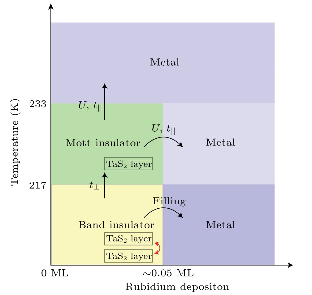
The phase diagram of 1T-TaS2is summarized in Fig.4.

Fig.4.Schematic depiction of the phase diagram of 1T-TaS2.Different phases are illustrated using different colors.Black arrows show the phase transitions driven by the modulation of interactions in different degrees of freedom.
4.Conclusion and perspectives
In summary,we show that the rubidium deposition drives two distinctive MITs at 205 K and 225 K in 1T-TaS2(Fig.4).Our results not only confirm that the LTIP is a normal band insulator,but also point out the existence of a Mott insulating phase at high temperature.This is consistent with the suppression oft⊥in the HTIP[17]and also the observation of Mottness in monolayer 1T-TaS2and 1T-TaSe2,[32-34]suggesting that the insulating property of 1T-TaS2originates from both the Mott localization and interlayer dimerization.By reducing thet⊥via temperature or reducing the layer thickness, a band-insulator-to-Mott-insulator transition occurs.Along the doping axis, the band gap or interlayer dimerization of the LTIP is robust against rubidium doping.The metallic state is achieved below 217 K by doping a band insulator.On contrary, the interlayer dimerization is absent above 217 K.A small amount of rubidium deposition leads to a collapse of the Mott gap.A metallic state is achieved at 225 K whose band structure resembles the metallic state above the C-CDW transition.Our results thus show that the metallic, band insulating and Mott insulating phases intersect in a small temperature and doping region in the phase diagram of 1T-TaS2(Fig.4).In this region,t‖,t⊥, andUmaintain a delicate balance in 1T-TaS2,making the electronic properties of 1T-TaS2very sensitive to various perturbations.Such a high sensitivity of 1T-TaS2to both temperature and rubidium deposition could be potentially used in constructing 2D functional phasechanging devices.[19-22,35-37]
Acknowledgements
Project supported by the National Natural Science Foundation of China (Grant Nos.11888101, 91421107, and 11574004) and the National Key Research and Development Program of China (Grant Nos.2018YFA0305602 and 2016YFA0301003).
- Chinese Physics B的其它文章
- Single-qubit quantum classifier based on gradient-free optimization algorithm
- Mode dynamics of Bose-Einstein condensates in a single-well potential
- A quantum algorithm for Toeplitz matrix-vector multiplication
- Non-Gaussian approach: Withstanding loss and noise of multi-scattering underwater channel for continuous-variable quantum teleportation
- Trajectory equation of a lump before and after collision with other waves for generalized Hirota-Satsuma-Ito equation
- Detection of healthy and pathological heartbeat dynamics in ECG signals using multivariate recurrence networks with multiple scale factors

