Method of simulating hybrid STT-MTJ/CMOS circuits based on MATLAB/Simulink
Min-Hui Ji(冀敏慧), Xin-Miao Zhang(张欣苗), Meng-Chun Pan(潘孟春), Qing-Fa Du(杜青法),Yue-Guo Hu(胡悦国), Jia-Fei Hu(胡佳飞), Wei-Cheng Qiu(邱伟成),Jun-Ping Peng(彭俊平), Zhu Lin(林珠), and Pei-Sen Li(李裴森),†
1College of Intelligence Science and Technology,National University of Defense Technology,Changsha 410073,China
2Beijing National Research Center for Information Science and Technology,Tsinghua University,Beijing 100084,China
Keywords: magnetic tunneling junction (MTJ) model, spin-transfer-torque (STT), circuit simulation, MATLAB/Simulink
1.Introduction
With the development of big data and internet of things(IoT), the problems of “memory wall” and “energy wall”caused by the von Neumann bottleneck are becoming increasingly prominent.Recently, spintronics has been regarded as one of the most important technologies to break the bottleneck, due to the advantage of non-volatile, low power, high speed, and compatibility with the traditional complementary metal–oxide–semiconductor (CMOS) devices.[1–4]The spintransfer-torque (STT) magnetic tunneling junction (MTJ) is one of the most important elements of spintronic technology,which can be used as magnetic memory,magnetic sensors,microwave transmitting and receiving devices.[5–9]The unique multiple functions from sensing, processing to communicating, open the way for the design of new types of computing in sensing devices and paradigms.[10]For example, the spin transfer nano-oscillators(STNOs)have been utilized for the development of new neuromorphic devices and computing paradigms.[11–13]And typically, the hybrid STT-MTJ/CMOS circuits need to be considered in the design process to make full use of advantages of MTJ technology and CMOS technology.Hence, a simulation model that captures the quasi-static and dynamic behaviors of STT-MTJ devices and a hybrid simulation framework of STT-MTJ/CMOS is urgently needed.[14]
Up to now,several hybrid STT-MTJ/CMOS models have been proposed, and most of them are programmed with the SPICE-based circuit simulators or Verilog-A compact model.[14–23]In 2012, Zhanget al.reported an compact perpendicular magnetic anisotropy (PMA) STT-MTJ model.[15]This model was programmed with the Verilog-A language.The tunnel resistance effect, the STT switching, and the stochastic behaviors were taken into account.Though this model provides an effective strategy for constructing memory and logic chips, it is personalized for the PMA MTJ devices and the precessional motion is discarded, which is one of the most important characteristics for the design of new generation of neuromorphic devices and oscillator-based computing.[24,25]For the simulation of in-plane magnetic anisotropy (IMA) STT-MTJ, in 2012, Yanget al.proposed a modified nodal analysis model with identified internal state variables in SPICE-like simulator,[16]which can deal with the dynamic behavior of devices under arbitrary driving condition,however the model parameters are not directly corresponding to the actual device parameters.Therefore, a timely and comprehensive STT-MTJ model is needed, which can easily adapt to different MTJ parameters and process technologies.Hence, In 2013, Panagopouloset al.developed a physicsbased SPICE compact hybrid MTJ/CMOS simulator.[17]The model of MTJ is implemented by using the only inbuilt components (voltage-dependent current sources, capacitors, and resistors), the dynamic behavior of MTJ was calculated by Kirchhoff’s law.This model provides the ability to predict the real magnet dynamic behaviors of IMA device and PMA STT-MTJ device.Similarly, Kazemiet al.reported an adaptive compact MTJ model[18]in 2014,which includes not only the STT effect, but also the voltage controlled magnetic anisotropy(VCMA)effect.This model can also be adapted to IMA and PMA MTJ.Both the models can predict devices’performances from material to circuit level.However,the SPICEbased model using the inbuilt components generally consists of many circuit components or electrical nodes,which are relatively complex.
Simulink provides an interactive graphical model environment and covers the most commonly used SPICE compatible models, which enables rapid construction of a simulation model to explore the design concepts from device to system level.Therefore, in this work, we propose an MATLAB/Simulink based framework for simulating hybrid STT-MTJ/CMOS circuits.The proposed model consists of a physics-based macrospin model of the STT-MTJ device, a controlled resistor,and a current sensor.The STT-MTJ model is edited using the MATLAB script, and the output of the script adjusts the resistance of the controlled resistor, while the current flowing through the controlled resistor will be fed back to STT-MTJ device.Benefited from the modular design of Simulink, the model can be easily expanded by creating a new physical module.Compared with the conventional SPICE-based physics hybrid STT-MTJ/CMOS method,the model presented in this paper is simple,very flexible,and easy to comprehend.
The remainder of this paper is organized as follows.In Section 2 the basic theory and key physics are described,and then the simulation framework based on MATLAB/Simulink is discussed.In Section 3 our proposed model is verified by using experiment results,and the simulation results including the hybrid STT-MTJ/CMOS circuit and the coupling of two devices are also shown.Finally, some conclusions are drawn in Section 4.
2.The simulation framework: Theory and key physics
2.1.MTJ construction and basics
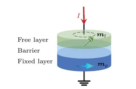
MTJ is a magnetic device consisting of an ultra-thin barrier layer and two ferromagnetic(FM)layers: one has a fixed magnetic orientation (fixed layer), whereas the other (free layer) can change its magnetic orientation.The device structure of MTJ is shown in Fig.1.The magnetization vector of the free layer and fixed layer are indicated bymfandmp,respectively.As is well known, the conductance (G) of the MTJ depends on the angle(θ)between the two magnetization vectors,can be calculated from.[9,26]
whereGPandGAPare the conductance of the MTJ device when the magnetic orientations of the two ferromagnetic layers are parallel(P)and antiparallel(AP)to each other,respectively.When the free layer is parallel to the fixed layer, the resistance of MTJ is in the minimum(RP=1/GP)state,while the device is in the high resistance state(RAP=1/GAP)when the relative magnetic orientations are antiparallel.The TMR ratio can be represented by the following equation,which decreases with the bias voltageVbiasincreasing:[27]
where TMR is the measured real value, TMR(0) is the TMR value when the bias voltage is close to zero,andVhis the corresponding bias voltage when TMR=0.5×TMR(0).

Fig.1.Basic schematic diagram of MTJ structure consisting of a free layer,a barrier layer,and a fixed layer.
2.2.Theories of magnetization dynamics
The free layer magnetization is macrospin approximately in our model.[28]The magnetization precession motion can be explained by the Landau–Lifshitz–Gilbert(LLG)equation with the additional Slonczewski’s term,[16,29,30]and the equation is shown as follows:
Here,mfandmpare the reduced magnetization vectors of the free layer and unit polarization direction of fixed layer,respectively,γis the gyromagnetic ratio,Heffis the effective field,αis the Gilbert damping factor,αJis the STT coefficient,andβJis the field-like torque coefficient.In the definition ofβ,Jis the current density, and it is assumed to be uniformly distributed on the surface.In this work, positiveJis defined as electrons flowing from the fixed layer to free layer, ¯his the reduced Planck constant,µis the vacuum permeability,eis the electronic charge,Msis the saturation magnetization, andtis the thickness of the free layer.The polarization functiongis dependent on the angle betweenmfandmp,Pis the spin polarization factor,Λis the torque asymmetry parameter,andεis the secondary spin transfer term.The effective fieldHeffcan be expressed as the sum of several different fields,including the applied external magnetic field (Hext), the effective uniaxial anisotropy field(Hk),the demagnetization field(Hd)and the thermal noise field(Hth)[31]as follows:
whereKuis the effective uniaxial anisotropy coefficient;Nis the demagnetizing factor, which depends on the shape and size of the free layer;[32]χis a three-dimensional Gaussian distribution with a zero mean and standard deviation,kBis the Boltzmann constant,Tis the temperature,Vis the volume of the computational cell,andδtis the simulation time step.
2.3.MATLAB/Simulink implementation
The proposed hybrid simulation framework can be divided into two main modules: the first is the simulation of the physics-based STT-MTJ model and the second is the analysis of the controlled resistance and peripheral circuit as shown in Fig.2.

Fig.2.Proposed hybrid MTJ-STT/CMOS modeling framework.
For the simplicity of simulation hybrid STT-MTJ/CMOS circuit, a MATLAB function block is used and the physicsbased STT-MTJ model is edited using the MATLAB script.First, the external magnetic fieldHextshould be offered, the initial magnetization states of free layer(mf0),the fixed layer magnetization vector(mp)and physical size of the device(l:length,w: width, andt: thickness) are input.The magnetic internal parameters mentioned above (Ms,α,P,Ku,T,...)are preset.And the effective field mentioned above(Eqs.(4)–(7))are considered in the simulation of the physics model.The LLGS equation is solved by using the improved Euler method.Therefore,the free layer magnetization vector(mf)can be obtained and the resistance (R) of the device can be calculated from Eqs.(1)–(3), as shown in the green part of Fig.2.The calculated resistance valueRis converted into a physical signal by using the Simulink-PS converter block.Therefore,the calculated valueRthat can control the resistance of the physically controlled resistor,changes fromRPtoRAP.The electrical ports of the controlled resistor can be connected with other semiconductor devices and electrical sources.Furthermore,the current sensor is used to obtain the current in the electric circuit.Then, the PS-Simulink converter block converts the physical current into the Simulink signalIin,which is used as an input current of the physics-based STT-MTJ model.
3.Simulation results
3.1.Physics-based STT-MTJ model
In this subsection, the proposed physics-based STTMTJ model is verified with the experimental result.The devices studied here have the following stack bottom electrode/PtMn(15)/Co70Fe3(2.3)/Ru(0.85)/Co40Fe40B20(2.4)/MgO(0.8)/Co20Fe60B20(2.0)/top electrode (numbers in bracket denotes the thickness in unit nm),and then the stacks are fabricated into pillar shaped device with the cross-section area of 100 nm×120 nm×π/4.The schematic diagram of the STT-MTJ device stacks is illustrated in Fig.3(a).And the measured typical resistance curve scan as a function ofIis shown in Fig.3(b)(the black curve).
The simulation is conducted by sweeping the currentIin steps ofδI.And under each current, the LLGS model is solved with a fixed time step ofδt.After each time step,the instantaneous resistanceR(t)is calculated.Based on this,the time-averaged resistance is used to evaluate the resistance for eachI.The red curve shown in Fig.3(b) represents the device’s switching characteristics calculated by using the parameters in the third column of Table 1 (switching behavior simulation values), and the values ofRPandRAPare 1 kΩand 2 kΩ, respectively.The results show that our proposed model can capture the dynamic switching characteristics accurately.Figures 3(c) and 3(d) show the time-domain transient resistance values and the magnetization precession threedimensional (3D) trajectories of the device at different bias currents.It can be observed that atI=0.3 mA,the resistance is equal toRP, and the precession of the free layer is aroundmp.As the current decreases to−0.54 mA, the STT-MTJ switches fromRPtoRAP.Themfprecesses around thempinitially,and finally stabilizes in the antiparallel direction.The resistance in antiparallel state is affected by the voltage, and the resistance is about 1800 Ω atI=0.06 mA.As the current reaches 0.08 mA,the resistance drops fromRAPtoRP.

Fig.3.(a)Schematic illustration of STT-MTJ device,(b)measured and simulated variation of resistance with current of STT-MTJ,with Hext equaling 0 Oe(the unit 1 Oe=79.5775 A·m−1),(c)time-dependent resistances,and(d)free layer precession 3D trajectories of the STT-MTJ device at different input currents.

Table 1.Parameters for simulating STT-MTJ switching and oscillation behaviors.
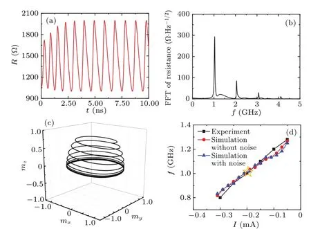
The STT-MTJ model used for analyzing the microwave oscillation characteristics is based on the experimental data presented by Zenget al.[33]For the large interfacial perpendicular anisotropy,the stable oscillation can be achieved without an external magnetic field.The parameters used to match the sustained oscillations are listed in the last column in Table 1(oscillation behavior simulation values)and the interfacial perpendicular anisotropy is included in the effective uniaxial anisotropy.Figure 4(a) shows the time-dependent transient resistance with the input currentI=−0.2 mA (the total simulation time is 60 ns, to observe the change of resistance clearly, only the results within 10 ns are shown here).Figure 4(b) shows the FFT result of the transient resistance.As can be seen from the figure, the fundamental frequency is 1.01 GHz.The 3D trajectory of themfmagnetization is shown in Fig.4(c), which is initially circular and gradually evolves into stable out-of-plane precession orbits.Figure 4(d)shows the microwave oscillation fundamental frequency as a function of bias current.The black curve is the experiment result reproduced from Zenget al.’s work,[33]the red circles and blue triangles show the simulation results based on our framework without and with the thermal noise, respectively.Note that the simulation results are consistent with the experimental results, and the oscillation frequency decreases with the increase of absolute current value at a rate of about 1.78 GHz/mA, demonstrating the validity of our proposed physics-based STT-MTJ model.

Fig.4.(a)Resistance,(b)resistance spectrum,and(c)free layer precession 3D trajectory of STNO device when the input current is −0.2 mA.(d)STNO oscillation fundamental frequency as a function of I with and without thermal noise with Hext equaling 0 Oe,the point marked in pentagram indicating that the corresponding frequency is 1.01 GHz when the input current is−0.2 mA.
3.2.Devices level simulation
For the hybrid simulation of STT-MTJ/CMOS circuits,our proposed framework is used to simulate the pre-charge sense amplifier(PCSA)circuit proposed by Zhaoet al.[34]The circuit is composed of two STT-MTJ devices, three NMOS transistors and four PMOS transistors.The circuit can sense the magnetic configuration of the MTJ at a high speed.Figure 5(a) shows the schematic of the proposed circuits, whereRPandRAPof the STT-MTJ device are 4.7 kΩ and 11.7 kΩ,respectively, and the remaining magnetic parameters are the same as the switching behavior simulation values.Moreover the parameters of the transistors are based on the 90-nm BSIM4 model.[35]The control signals and the corresponding simulation results are shown in Fig.5(b).It is observed that when “SEN” is set to zero, the polarization voltages of the two MTJs,QmandQm_barare both equal toVdd.And when“SEN”changes to a high level,both two voltages begin to decrease due to MTJs discharging.The resistance of MTJ1 is set toRAP,whereas the resistance of MTJ0 isRP.Therefore, the discharge speed in the MTJ0 branch is faster than that in the MTJ1 branch.When the difference betweenQmandQmbaris less than the threshold voltage of P1, the P1 will be open andQm_Barwill be charged toVdd,whileQmwill continue discharge to zero potential.The simulation result is consistent with the result in Ref.[34].

Fig.5.(a)PCSA circuit consisting of STT-MTJ devices,three NMOS transistors and four PMOS transistors,(b)control single(SEN)and the simulated voltage results of Qm and Qmbar.
The coupling of the STNOs is a promising component for neuromorphic computing and associative memory.[13]And our proposed framework can emulate the coupling characteristics of the STNO conveniently.Figure 6(a) shows the electrical coupling simulation method of two STNOs.[4]The simulation parameters are the same as the ones listed in Table 1 (oscillator behavior simulation values).The independent bias currents(Ibias1andIbias2)and external magnetic fields(Hbias1andHbias2) are applied to STNOs.By appropriately controlling the bias current and external magnetic field, the microwave signal can be generated,and the devices are coupled with each other.TheIbroadcaston the feedback branch is calculated from the following equation:
whereC1andC2are the coupling constants, which are determined by the coupling circuit;mx1andmx2are free layer magnetizationx-direction components.The currents flowing through the STNO areIinput1andIinput2, respectively.Therefore, the input current is the combination of the bias current and feedback current
Based on the proposed electrical coupling simulation method, in order to analyze the coupling behavior, the bias current and external magnetic field are changed independently.First, the bias currents of both STNOs are kept at−0.2 mA.The external magnetic field,perpendicular to plane free layer,of STNO2 is constant at a zero magnetic field,while the magnetic field sensed by STNO1 changes from−3 mT to 3 mT.For a non-zero coupling coefficient(C1=C2=0.01),the frequency of the two STNOs is locked in a suitable magnetic field range from−0.6 mT to 0.6 mT.The simulation results are shown in Fig.6(b).In addition,the external magnetic field of the two STNOs is set to 0 mT,theIbias2is set to−0.2 mA,while theIbias1is varying.The coupling coefficients remain unchanged.The oscillation frequencies of the two STNOs are shown in Fig.6(c), which demonstrate the same rules as unilaterally changingHbias1.

Fig.6.(a)Schematic diagram of two STNOs with electrical coupling,STNO oscillation frequencies as a function of(b)magnetic field applied perpendicular to the plane of free layer and(c)bias current under constant zero magnetic field(T =0 K).
4.Conclusions
This work presents a hybrid STT-MTJ/CMOS model framework based on MATLAB/Simulink, which is mainly composed of a physics-based STT-MTJ model, a controlled resistor, and a current sensor.The physics model developed under the single domain approximation is benchmarked with experimental results.Based on the proposed hybrid STTMTJ/CMOS model framework, the PCSA circuit consisting of two STT-MTJ devices and the coupling of two STNOs are simulated.The simulation results are consistent with the published results.It is pointed out that the model is applicable to both IMA device and PMA STT-MTJ device by presetting the direction of fixed layer and uniaxial anisotropy parameter.Our proposed model paves the way for the hybrid STTMTJ/CMOS simulation of device, circuit, and system architecture,including not only the design of spin-based logic and memory devices, but also the development of the neuromorphic devices and oscillation-based computing framework.
Acknowledgements
Project supported by the National Natural Science Foundation of China (Grant No.62004223), the Science and Technology Innovation Program of Hunan Province, China(Grant No.2022RC1094), the Open Research Fund Program of the State Key Laboratory of Low-Dimensional Quantum Physics,China(Grant No.KF202012),and the Hunan Provincial Science Innovation Project for Postgraduate,China(Grant No.CX20210086).
- Chinese Physics B的其它文章
- First-principles calculations of high pressure and temperature properties of Fe7C3
- Monte Carlo calculation of the exposure of Chinese female astronauts to earth’s trapped radiation on board the Chinese Space Station
- Optimization of communication topology for persistent formation in case of communication faults
- Energy conversion materials for the space solar power station
- Stability of connected and automated vehicles platoon considering communications failures
- Lightweight and highly robust memristor-based hybrid neural networks for electroencephalogram signal processing

