Improved performance of MoS2 FET by in situ NH3 doping in ALD Al2O3 dielectric
Xiaoting Sun(孙小婷), Yadong Zhang(张亚东), Kunpeng Jia(贾昆鹏), Guoliang Tian(田国良),3, Jiahan Yu(余嘉晗),Jinjuan Xiang(项金娟), Ruixia Yang(杨瑞霞), Zhenhua Wu(吴振华),3,†, and Huaxiang Yin(殷华湘),3,‡
1School of Information Engineering,Hebei University of Technology,Tianjin 300401,China
2Key Laboratory of Microelectronics Device and Integrated Technology,Institute of Microelectronics Chinese Academy of Sciences,Beijing 100029,China
3University of Chinese Academy of Sciences,Beijing 100049,China
Keywords: MoS2,Al2O3 dielectric,NH3 in-situ doping,oxygen vacancy
1. Introduction
In 2004, the discovery of graphene attracted much research attention to two-dimensional (2D) materials.[1]Graphene has an ultra-high mobility of up to 2×105cm2·V-1·s-1,[2]but its gapless nature limits its applications in the field of electronic transistors. Alternative transition metal dichalcogenides(TMDs)with atomic thickness and a tunable bandgap can overcome the shortcomings of graphene and demonstrate unique optical and electrical properties.[3–6]Molybdenum disulfide (MoS2), one of the most widely studied TMDs,shows a variety of bandgaps from 1.2 eV to 1.9 eV with films from bulk to monolayer.[7]The fabricated MoS2field-effect transistors (FETs) show high carrier mobility,[8]high on–off ratios[9]and excellent subthreshold swing,[10]and have great possibilities for application in a variety of electronic devices, such as sensors,[11]photodetectors,[12]and logic devices.[13]
Theoretically, the intrinsic mobility of MoS2FETs can reach 410 cm2·V-1·s-1,[14]but in practice the reported mobility is far less than that. There are many scattering mechanisms in the devices,including charged impurity(CI)scattering,one of the most important factors that degrades mobility.[15]For a back-gate structure FET, the interface states between the 2D channel material and the gate dielectric can be improved by using a high-κdielectric instead of SiO2to provide a special passivation process for effectively screening CI scattering. Many experimental results also show that MoS2FETs with high-κgate dielectrics, such as HfO2,[16]ZrO2,[17]and Al2O3,[18]exhibit good electrical performance. However,the oxygen vacancies and dangling bonds distributed on the surface of high-κdielectrics lead to the interface-state density of dielectrics/MoS2reaching 1011–1012cm-1·eV-1.[19]Recently, much effort has been made to decrease the interfacial defects,such as various plasma treatments(O2,N2,NH3,and CF4/O2),[20–23]rapid thermal annealing (RTA)[24,25]and dielectric-mediated doping[26]after the deposition of high-κfilms. Proper nitrogen doping into the dielectrics during the deposition process supplies an effective way to improve the quality of the dielectrics.[27]Compared with treatments after growth,in situdoping is easier and effective. However,no research has yet been reported onin situNH3doped Al2O3as a gate dielectric in MoS2FETs. In this work, MoS2FETs with NH3doped atomic layer deposition (ALD) Al2O3are systemically explored. Through x-ray photoelectron spectroscopy (XPS) and atomic force microscopy (AFM) characterization and electrical tests,the effects of different sequences of NH3doping into the gate dielectric on device performance are investigated. The results show that MoS2FETs with ALD Al2O3doped with NH3during the final stages demonstrate the best performance;this is consistent with the results of dielectric analysis.
2. Experiments
In the FET experiments, a heavily doped p++ Si (100)8inch wafer was used as the back gate. The gate dielectric was formed from an ALD Al2O3thin film grown at 300°C using trimethylaluminum(TMA;Al(CH)3)and H2O as Al and oxygen precursors, respectively. Firstly, TMA vapors are pulsed into the chamber and adsorb on the substrate surface,followed by pulsing of N2into the chamber to purge the unabsorbed TMA.Then H2O vapors are pulsed to react with TMA to generate Al2O3and other by-products. At the end of the cycle,N2is pumped in to remove excess gas and any other gases produced. The control of the film thickness is achieved by changing the number of cycles. In this work, the growth rate of the undoped Al2O3film is 1.05 ˚A/cycle and a 20 nm thick film is grown after 190 cycles. To realize nitrogen doping in the Al2O3dielectric layer, different sequences for introducing NH3into the growth cycle were designed in this experiment, as shown in Fig. 1. The growth sequence TMA–N2–H2O–N2–NH3–N2is called AlON (0.89 ˚A/cycle, 224 cycles for 20 nm)and the sequence TMA–N2–NH3–N2–H2O–N2is called AlNO(1.05 ˚A/cycle,190 cycles for 20 nm).
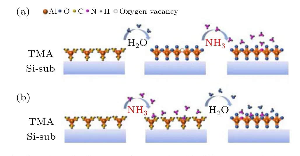
Fig. 1. Schematic diagrams of one cycle with different NH3 doping sequences.
The MoS2flake channel material was mechanically exfoliated from bulk MoS2crystal(purchased from Six Carbon Technology,Shenzhen)using scotch tape and then transferred onto the target substrate by PDMS. Next, lithography with a negative polymer resist was used to define the source/drain region. Then, the metal electrode (Ti/Au=10/40 nm) was deposited by electron beam evaporation, and the metal was stripped by lift-off to form a separate metal electrode.
Figure 2(a) is a schematic diagram of a few-layer MoS2FET with a 20 nm Al2O3gate dielectric and Ti/Au electrodes.The prepared MoS2FET is shown in Fig.2(b),and the length and width of the channel are 3 μm and 10.86 μm,respectively.The thickness of MoS2measured by AFM is 6 nm,as shown in Fig. 2(c). Figure 2(d) shows the Raman spectra of the MoS2flake and the Raman shift between the E12gpeak (384 cm-1)and the A1gpeak(408 cm-1)is 24 cm-1.
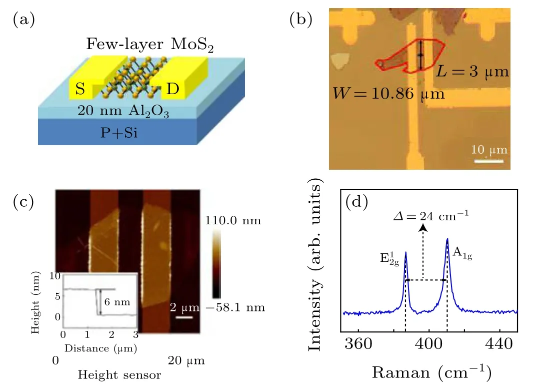
Fig.2. (a)Schematic of a few-layer MoS2 FET with a 20 nm Al2O3 gate dielectric and Ti/Au electrodes. (b)Optical photograph of the prepared MoS2 transistor. (c)AFM image of the MoS2 transistor with the inset showing the thickness of the MoS2 flake measured by AFM.(d)Raman spectra of MoS2 flake.
The high-frequency(1 MHz)capacitance–voltage(C–V)curves and the electrical characteristics of MoS2FETs were measured using a Keithley 4200-SCS and an Agilent 4156C,respectively, at room temperature in an atmospheric environment.
3. Results and discussion
The influence ofin situNH3doping on the dielectric was explored with theC–Vtest. A metal,a gate dielectric(Al2O3,AlON, AlNO) and Si form a metal–oxide–semiconductor(MOS) capacitor structure. TheC–Vcurves of MOS capacitors measured at 1 MHz are shown in Fig.3(a). For the gate dielectrics Al2O3, AlON and AlNO, the MOS oxide capacitances per unit area (Cox) are 0.337 μF/cm2, 0.381 μF/cm2,and 0.357 μF/cm2, respectively.Coxis increased by the use of NH3doping, indicating improvement of the gate control capability. Figure 3(b) shows thekvalues of the three dielectrics and capacitance equivalent thicknesses. Based onk=(Coxtox)/ε,in whichεis the vacuum permittivity andtoxis the thickness of the gate dielectric, thekvalues for Al2O3,AlON and AlNO are 7.6,8.6,and 8.1,respectively. It is found that NH3doping can improve thekvalue of the dielectric layer due to the incorporation of nitrogen. Meanwhile, the capacitance equivalent thicknesses are decreased,which is conducive to a reduction of device size without affecting the gate control ability. Figure 3(c)shows the gate leakage current under gate voltages from-1 V to 1 V. After NH3doping, the dielectric leakage current decreases and the leakage current of AlON is one order of magnitude lower than that of Al2O3. From the electrical characterization,it is obvious that various electrical parameters are improved after NH3is doped into Al2O3. This is mainly because NH3doping reduces the defects caused by oxygen vacancies.[28]However,the degree to which vacancies are suppressed is dependent on the sequence of NH3doping.When the film grows not as AlNO but as AlON,a better gate dielectric is obtained. An explanation for this is that the NH3doping sequence affects the bonding state of elements during the ALD process.
The surface roughness of the gate dielectric reflects the quality of the film.The roughness can affect the surface roughness scattering and thus the mobility of the carriers.[29,30]In this work, AFM is used to evaluate the root-mean square(RMS)roughness of the samples,as shown in Figs.4(a)–4(c).The RMS roughness of Al2O3,AlON and AlNO is 0.217 nm,0.169 nm, and 0.192 nm, respectively. Compared with the control sample Al2O3,samples with NH3doping have smaller RMS roughness. The AlON film has the best surface with the smallest surface roughness. This is consistent with the previous assumption that NH3doping and the sequence of doping have an impact on the quality of the dielectric layer.The flat surface is beneficial to improving the mobility of the carriers.[31]

Fig.3. (a)The C–V curves of MOS capacitors. (b)Relevant k values and capacitance equivalent thicknesses. (c)Gate leakage current(Jg)–Vg characteristics.

Fig.4.AFM height image(5 μm×5 μm)of the surface of the gate dielectric:(a)Al2O3,(b)AlON,(c)AlNO.
To further clarify the mechanism of NH3doping, XPS was used to analyze the chemical bonds of the three samples.In Fig.5,O 1s has various binding energies of common chemical states, among which the low binding energy (531.2 eV)corresponds to lattice oxygen derived from O–Al in Al2O3and non-lattice and surface oxygen have a higher binding energy(532.5 eV).[32]As shown in Figs. 5(a)–5(c), the red line represents lattice oxygen and the blue line represents non-lattice oxygen. The ratio of O-Al/Odefectin the film is reflected by the spectral peak intensity ratio and is 2.59, 4.42, and 3.91 in Al2O3,AlON and AlNO,respectively. Compared with the control sample Al2O3,the dielectric layers doped by NH3have a larger peak intensity ratio,representing the fewer oxygen vacancy defects which are repaired by nitrogen.
The XPS Al 2p spectra was extracted to analyze the bonding states of nitrogen and aluminum.As presented in Fig.5(d),there is only one spectral peak derived from the Al–O bond at 74.55 eV in the Al2O3dielectric layer. After the NH3doping, the peak of Al–N is visible at 73.31 eV, which indicates that nitrogen has been incorporated into Al2O3and formed Al–N bonds. The peak intensity of Al–N represents the number of bonds formed and the peak intensity in the AlON layer is stronger than that in the AlNO layer, which is shown in Figs. 5(e)and 5(f). Corresponding to the peak intensity ratio in Figs. 5(b) and 5(c), there are more Al–N bonds in AlON,which means that more vacancies are repaired. These results show the influence of different nitrogen doping sequences on the dielectric.
Furthermore,the electrical characteristics of MoS2FETs were measured to study the effect of NH3doping on device performance. Figure 6(a) shows the output characteristics of the three samples, and the scanning gate voltage ranges from-2 V to 4 V in steps of 2 V. The samples with NH3doping achieve a higher drain current and the device has the highest drain current (8.0 μA/μm) atVg=4 V with AlON as the dielectric layer. Due to the effect of NH3doping on the repair of oxygen vacancies, carrier scattering at the interface of the channel and the dielectric layer is reduced,resulting in higher carrier transport efficiency and a larger current.
Figure 6(b)shows the transfer characteristics of the three samples with normalized drain current in order to avoid the influence of channel width on the output current. The threshold voltagesVthextracted in Fig.6(b)are-0.74 V,-0.12 V,and-0.4 V for the samples with Al2O3,AlON and AlNO gate dielectric layers. It is obvious that theVthof a MoS2FET has a positive drift with a NH3-doped dielectric. Using Al2O3as the dielectric layer,a mass of oxygen vacancies with positive charges exist in the film, causing negativeVth.[33]After NH3doping into the high-κlayer,charge traps are repaired andVthhas a positive drift.[34]The sample with AlON has the smallest|Vth|, which also indicates that the MoS2/AlON interface has the fewest defective states.
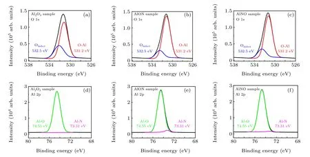
Fig.5. Deconvolution of XPS O 1s and Al 2p spectra of the three samples.
Figure 6(c) demonstrates the transfer characteristics in a semilog scale withVds=0.2 V,from whichIon/Ioffcan be extracted to be 1.33×105,3.56×106,and 1.06×10⁶for samples with Al2O3,AlON and AlNO,respectively. TheIon/Ioffof the sample with NH3doping is one order of magnitude larger than the sample without NH3doping. According to the above analysis,the repair of oxygen vacancy defects is helpful to reduce the carrier scattering capability,which can increaseIonand decreaseIoffof transistors. From Fig. 6(c), the value of subthreshold swing(SS)can also be extracted; it is 139 mV/dec,105 mV/dec,and 117 mV/dec for samples with Al2O3,AlON and AlNO,respectively. The sample with an AlON dielectric has the smallest SS,which is due to improvement of the interface quality after NH3doping.
In order to explore the carrier mobility trend of the device channel,decades of devices using Al2O3,AlON and AlNO as the gate dielectric are selected and the value is calculated by using the following equation:

in whichCoxis the oxide capacitance per unit area of the gate dielectric,LandWare the channel length and width, respectively,and ΔIds/ΔVgsis the slope of the transfer characteristic curve on a linear scale.As shown in Fig.6(d),it is obvious that the MoS2FETs with NH3-doped Al2O3have a higher carrier mobility.
In the process of Al2O3deposition it is inevitable that oxygen vacancies will be generated because of the low crystallization temperature of Al2O3.[35]The existence of vacancies tends to form charge centers,and thus the charge scattering effect of the dielectric layer is affected. By doping nitrogen into the dielectric layer,oxygen vacancies are substituted by nitrogen atoms, which effectively screen the CI scattering in the dielectric layer and thekvalue of the dielectric is increased.In addition, the introduction of NH3during ALD growth of Al2O3can also reduce the interface roughness of dielectric and channel materials,drastically decreasing the effect of interface scattering on channel carrier transport.
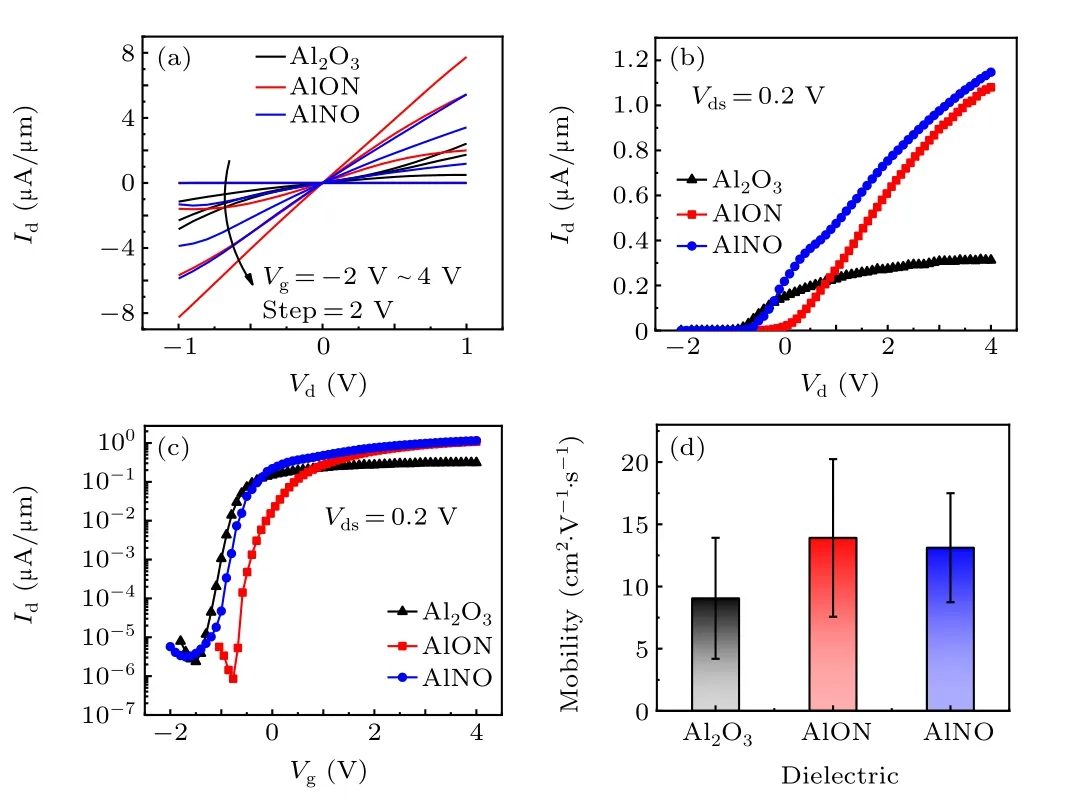
Fig. 6. (a) The Id–Vds curves in the linear region for the three samples. (b)Transfer characteristics of the three samples on a linear scale with Vds =0.2 V. (c) Transfer characteristics of the three samples on a semilog scale with Vds=0.2 V.(d)Average value of mobility of the three samples.
Figure 7 shows the off-state current and subthreshold swings of MoS2transistors produced using different treatment methods. Compared with other processes, the device in our work exhibits better performance and achieves a smaller SS(105 mV/dec)while maintaining a low off-state current.
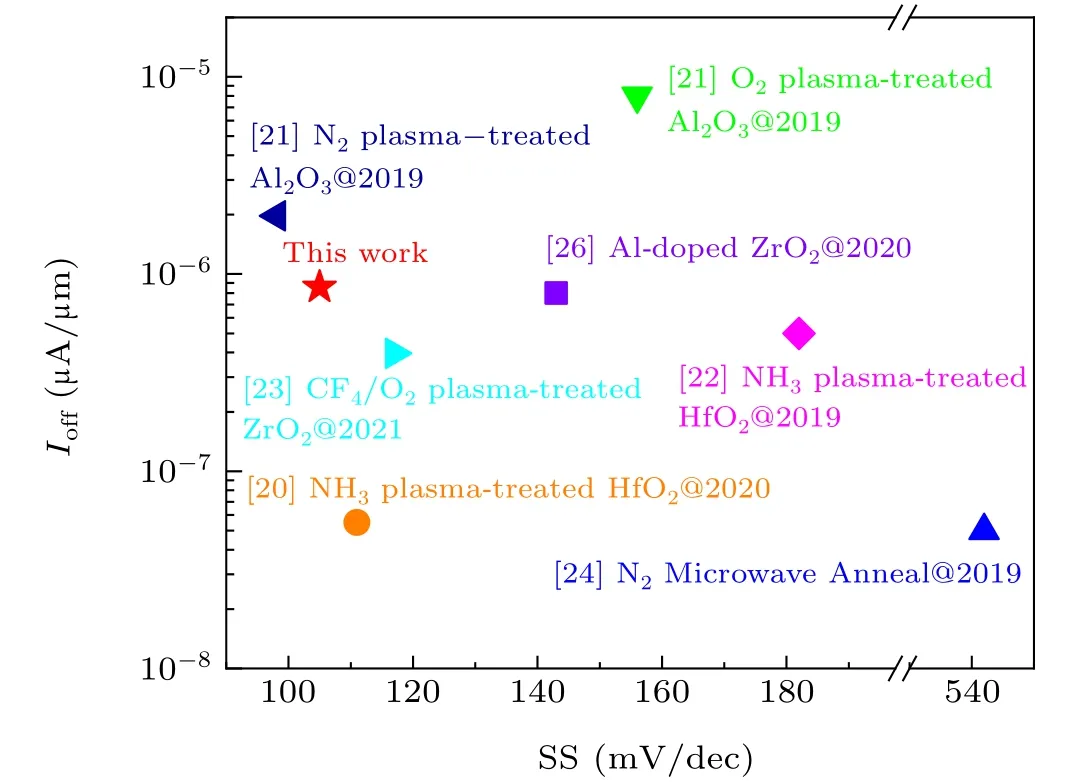
Fig. 7. A plot of off-state current versus the subthreshold swings from this work compared with MoS2 FETs treated with other reported processes.
4. Conclusion
In summary, the processing method and the impacts of NH3in situdoping into an Al2O3gate dielectric on MoS2FETs have been systematically investigated. Two different doping sequences were investigated in experiments. Through XPS and AFM characterization and the MOS capacitor electrical test, it was found that final doping of NH3during the ALD growth cycles demonstrates the best results. The oxygen vacancy defects in the Al2O3dielectric are repaired by thisin situNH3doping, and the carrier scattering of the interfaces between the gate dielectric and TMD channel material is obviously reduced. As a result, the performance of the MoS2FET is effectively improved,and the threshold voltage shift to an ideal state close to 0 V.Thein situdielectric treatment reported in this paper provides an effective and simple method to improve performance as well as the threshold control in the development of future TMD integrated circuits.
Acknowledgments
Project supported by the National Natural Science Foundation of China(Grant Nos.61774168 and 11764008)and the Opening Project of Key Laboratory of Microelectronic Devices & Integrated Technology, Institute of Microelectronics,Chinese Academy of Sciences.
- Chinese Physics B的其它文章
- Real non-Hermitian energy spectra without any symmetry
- Propagation and modulational instability of Rossby waves in stratified fluids
- Effect of observation time on source identification of diffusion in complex networks
- Topological phase transition in cavity optomechanical system with periodical modulation
- Practical security analysis of continuous-variable quantum key distribution with an unbalanced heterodyne detector
- Photon blockade in a cavity–atom optomechanical system

