Selective electrochemical etching of cantilever-type SOI-MEMS devices
Xiuchun Hao,Peiling He,and Xin Li
ABSTRACT It is possible to achieve selective electrochemical etching between different materials,such as p-and n-type silicon.However,achieving selective electrochemical etching on two different regions of the same p-type silicon material is a problem that has rarely been considered.Herein,a novel selective electrochemical etching technique for cantilever-type silicon-on-insulator(SOI)wafer-based microswitches is proposed.In this study,a p-type handle layer was selectively etched,and a p-type device layer was passivated.This was achieved using a circuit with two voltage sources:voltages of-1.2 and 0 V were applied to the handle and device layers,respectively.It was found that the proposed etching process can effectively prevent the in-use sticking of a cantilever-type switch.This is accomplished by increasing the gap between the device layer and its underlying handle layer and increasing the roughness of these layers.The technique is applicable to the fabrication of various cantilever-type SOI microelectromechanical systems,irrespective of the resistivity of the SOI wafer.©2022 Author(s).All article content,except where otherwise noted,is licensed under a Creative Commons Attribution(CC BY)license(http://creativecommons.org/licenses/by/4.0/).https://doi.org/10.1063/10.0010296
KEYWORDS SOI-MEMS,selective electrochemical etching,cantilever-type switch,sticking
I.INTRODUCTION
In recent years,an increasing number of microelectromechanical systems(MEMS)devices have been constructed using siliconon-insulator(SOI)wafers.However,a remaining issue with these devices is the so-called sticking problem,1,2which comes about for two reasons.The firs is the narrow size of the gap formed when the underlying SiO2sacrificia layer is removed to form a cantilever;the second is the low roughness of the surfaces of the two facing layers that contact.These fla surfaces and the narrow gap between them cause problems in the release process that limit the design flexibilit and applications of cantilever-type SOI-MEMS devices.Although several release techniques-such as sublimation drying,3supercritical drying,4photoresist-assisted release,5and vapor HF etching-have been applied to this problem,6these approaches are not effective for preventing in-use sticking.7,8
Researchers have proposed various strategies to solve this problem,but each has application limitations.For example,the creation of an inactive fil coating requires a special apparatus,9,10the fabrication of dimple structures is difficul to apply to cantilever SOI-MEMS systems,11and wet selective etching using HF-HNO3-CH3COOH has limitations in terms of the applicable resistivity values of the device and the handle layer.12A process involving electrochemical stop-etching of structures containing an-type layer of silicon formed by phosphorus diffusion for fabricating the membrane(beam)of silicon cantilevers has also been investigated.13
Of the techniques listed above,wet selective etching is simple,flexibl in operation,does not require special equipment,and has low cost.However,existing wet selective etching and electrochemical etching techniques are suitable for different types of silicon orp-type silicon with different types of impurity.When the materials of the device and handle layers of an SOI-MEMS device are identical,the ability to etch one layer while protecting the other is an area in need of study,and this is the subject of this paper.In this study,a novel selective electrochemical etching technique was used to fabricate a cantilever-type switch to prevent both fabrication sticking and in-use sticking.
II.MATERIALS AND METHODS
A.Fabrication of cantilever-type switch
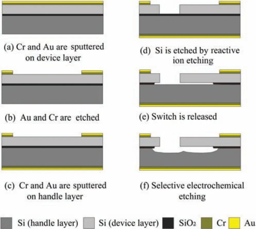
As an example of the proposed technique,a cantilever-type touch switch was fabricated.The material was a〈100〉-orientedp-type SOI wafer with a 5-μm-thick device layer,a 450-μm-thick handle layer,and a 1-μm-thick buried SiO2layer.The resistivity of both the device and handle layers was 0.02Ωcm.The principle of the cantilever-type switch is shown in Fig.1.When a load is applied to the cantilever,the switch makes contact in the“on”position.Figure 2 shows the process of the switch fabrication.Steps(a),(b),and(c)form the surface and backside electrodes.Chromium and gold(Cr/Au)are the electrode materials.Steps(d)and(e)form the cantilever.The fina step(f)is a silicon-selective etching process to roughen the mirror-like surface of the substrate.
B.Experimental design
The electrochemical etching of silicon(bothpandndoped)in KOH is controlled by the bias potential(see theI-Vcurve in Fig.3).14When the potential applied to the silicon is less than the passivation potential(PP),it will be etched.When the applied potential is equal to or larger than the PP,anodic oxidation will occur.In our research,only roughening of the handle layer was desired.Selective etching is required to prevent the device layer being inadvertently etched.Selective electrochemical etching is achieved by use of a reverse-biased SOI device.When the device layer is biased with a positive potential(>PP)compared to the solution and the handle layer is at its open circuit potential(OCP),the device layer will not be etched due to the anodic bias,but the handle layer will.

FIG.1.Cantilever-type structure.

FIG.2.Steps in the process of fabricating a cantilever-type switch.

FIG.3.Electrochemical I–V characteristics during electrochemicaletching.
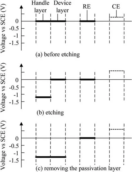
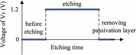
In our system,which is shown schematically in Fig.4,a four-electrode apparatus was used for electrochemical etching at 60○C with 40 wt.%KOH solution.This system used a platinum(Pt)counter-electrode,a saturated calomel electrode(SCE)as a reference electrode(RE),and the handle and device layers of the cantilever switch as working electrodes.A potentiostat(CHI660E)was connected to the positive terminal of a second voltage sourceVE(VICTOR VC3003A)and the device layer,and the negative terminal of this voltage source was connected to the handle layer.The bias potentials of each electrode during the different stages of the etching process are shown in Fig.5.Agraph of the voltage supply during the etching process is shown in Fig.6.

FIG.4.Four-electrode selective electrochemicaletching system.

FIG.5.Bias potentialof each electrode in the etching process.RE:reference electrode;CE:counter electrode.

FIG.6.Variation ofthe supply potentialduring the etching process.
Before electrochemical etching began,the potentials of the two working electrodes were set to the PP.In our experiment,the PP was 0 V relative to the RE.When selective electrochemical etching was started,a suitable voltage near to the OCP ofp-type silicon(-1.2 V relative to the RE)was applied directly to the handle layer to ensure that it maintained a controlled etching potential.The second voltage supplyVEwas used to bias the device layer at the PP,i.e.,>1.04 V(refer to Fig.3)with respect to the RE(the PP forp-type silicon).In practice,VEwas set to about 1.2 V,which puts the device layer at 0 V with respect to the RE when the handle layer is etched.Finally,to avoid the influenc of the passivation layer on the electrical characteristics of the cantilever switch,VEwas adjusted to 0 V,and the device layer was set at-1.2 V.In this way,the device layer and the handle layer will be synchronously etched.The electrochemical etching was terminated as soon as the device layer began to be etched.
III.RESULTS AND DISCUSSION
A.Roughness of the handle layer
To release the switch,it is necessary to remove the buried oxide layer by etching.In our experiments,the vapor hydrofluori acid(HF)and aqueous HF releasing techniques were used to remove the oxide layer.The RMS roughness of the released handle layer was about 1.2 nm.After releasing,the switch device was selectively electrochemically etched.A scanning electron microscope(SEM)image(obtained using a Hitachi S-3400N)of one of the fabricated switches is shown in Fig.7(a).The RMS roughness of the handle layer was increased after selective electrochemical etching;this was~82.9 nm after etching with vapor HF[Fig.7(b)],and it was~18.6 nm after etching with aqueous HF[Fig.7(c)].
The reason for the different roughnesses after the cantilever was released using the vapor HF or aqueous HF techniques is suggested to be as follows.The process for the vapor-HF releasing technique is described by the following set of chemical equations:

In these equations,“g”indicates gas and“ads”indicates adsorbed.Equation(3)shows that,in the etching process,redundant H+is left on the handle layer after vapor HF etching.When the etching is started,the H+adsorbed on the handle layer will react quickly with the OH-in the KOHsolution,resulting in an inconsistent etching rate on the surface of the whole handle layer.The result is that the substrate regions where H+was adsorbed are deeply etched.Therefore,when the handle layer is electrochemically etched with vapor HF,it is rougher than when etched with aqueous HF.
The above analysis was confirme by the following experiment.A〈100〉-orientedp-type silicon wafer with a 1-μm oxide layer was electrochemically etched after the removal of the oxide layer by a different method.Optical images(obtained using an Olympus BX53 light microscope)of the surface before and after electrochemical etching are shown in Fig.8.The figure on the left in(a)-(d)show different treatments for the oxide layer.From(a)to(d)respectively indicate that the oxide layer is etched by HF solution,the oxide layer is etched by HF vapor for 30 minutes,the oxide layer is etched by HF vapor for 60 minutes,and the oxide layer is etched by HF vapor for 150 minutes.The roughness values after electrochemical etching from Figs.8(a)-8(d)are 12.1,25.2,68.7,and 91.2 nm,respectively.The surface where vapor HF oxide etching was employed is rougher than that etched with aqueous HF.For the surface etched with HF vapor,the roughness increased with the etching time.

FIG.7.SEM images of the fabricated device:(a)whole device;(b)handle layer after electrochemicaletching with vapor HF;(c)handle layer after electrochemicaletching with aqueous HF.

FIG.8.Opticalmicrographs ofsurfaces before and after electrochemicaletching with different methods.ECE:electrochemicaletching for 10 min.(a)Oxide etching with HF solution.(b)Oxide etching with HF vapor for 30 min.(c)Oxide etching with HF vapor for 60 min.(d)Oxide etching with HF vapor for 150 min.
B.Detachment length and gap
Touch switches with lengths and widths of 100,300,and 500μm were fabricated.The detachment length of the fabricated cantilevers was increased from 100μm(before electrochemical etching)to 500μm after 4 min of electrochemical etching with aqueous HF,and the gap between the cantilever and the substrate was increased from 1.00 to 1.25μm.As summarized in Table I,the validity of the selective electrochemical etching technique in preventing fabrication sticking was confirmed Even for 100-μm lengths,the cantilevers released with vapor HF did not stick.
C.Pressure required to cause sticking
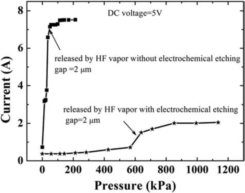
A distributed load was applied to each of the fabricated switches,as shown schematically in Fig.9.For a given voltage,the pressure required to cause sticking can be measured as a function of the current and the applied load;if a switch does not stick,then the current will gradually increase with the applied load.If a switch does stick,then the current will remain almost unchanged as the applied load increases until the switch is broken.Measurement results taking a switch with a length of 300μm and a width of 500μm as an example are shown in Fig.10.For the switch without electrochemical etching,the pressure required to cause sticking was 35.5 kPa.For the switch with electrochemical etching by vapor HF,this value was 639 kPa.The pressure required to cause sticking was thus increased with selective electrochemical etching.In our tests,the applied load on the switch was 0.03 N.The applied pressure was thus 200 kPa for a switch of 300μm length and 500μm width.This is less than the pressure that caused sticking.

TABLE I.States ofcantilevers before and after electrochemicaletching for 4 min.

FIG.9.Schematic diagram of the apparatus for the in-use sticking test.

FIG.10.Relationship between currentand applied distributed load.
IV.CONCLUSIONS
Herein,we propose an electrochemical etching technique that can achieve the selective etching of different parts of the samep-type silicon material irrespective of resistivity.Cantilever-type switches with various sizes were fabricated using this new approach.The handle layer was roughened by the selective electrochemical etching.Different methods for etching the buried oxide layer affected the roughness of the handle layer differently:etching with HF vapor produced a rougher handle layer than etching with aqueous HF.The gap between the movable parts of the switch and the substrate was increased.The maximum detachment length of the fabricated cantilever before and after electrochemical etching was increased from 100μm to more than 500μm.The effectiveness of selective electrochemical in preventing release sticking was confirme by comparing the detachment length.The effectiveness of selective electrochemical etching in preventing in-use sticking was also confirme through the relationship between the current and the applied distributed load.It can thus be said that selective electrochemical etching could be effective for preventing both fabrication sticking and in-use sticking of cantilever-type switches or other SOI-MEMS devices.
ACKNOWLEDGMENTS
This work was supported by the National Natural Science Foundation of China(Grant Nos.51575248 and 32071900).
AUTHOR DECLARATIONS
Conflict of Interest
The authors have no conflict to disclose.
DATA AVAILABILITY
All data included in this study are available upon request by contact with the corresponding author.
- 纳米技术与精密工程的其它文章
- Manipulations of micro/nanoparticles using gigahertz acoustic streaming tweezers
- A button switch inspired duplex hydrogel sensor based on both triboelectric and piezoresistive effects for detecting dynamic and static pressure
- Extraction algorithm for longitudinal and transverse mechanical information of AFM
- Dynamic performance of a long-stroke fast tool servo system
- A review of anomalous refractive and reflective metasurfaces

