
First principles study of field effect device through van der Waals and lateral heterostructures of graphene, phosphorene and graphane
2022-04-13 04:07:52RebolledoEspinozaRyndykDianatGutierrezuniberti
Namo Materials Science 2022年1期
. Rebolledo Espinoza, D.A. Ryndyk, A. Dianat, R. Gutierrez, G. uniberti
Chair of Materials Science and Nanotechnology, TU Dresden, 01069, Dresden, Germany
Keywords:2D materials van der Waals heterostructure Graphene Phosphorene Graphane DFTB Defects Field effect
ABSTRACT Chemical modification and vertical stacking of two-dimensional materials are promising techniques for new nanoelectronic devices. We present Density Functional Tight Binding(DFTB)calculations of a field-effect device,based on lateral and vertical heterostructures of 2D materials. The device consists of a phosphorene channel protected by graphene sheets, which work as contacts and are divided into the source and drain by local hydrogenation of graphene,which gives insulating graphane.In this device composed of only 3 layers,single sheets of graphene-graphane can work as both leads and oxide gate, while also acting as protective layers for a phosphorene channel. We show how for perfect vdW heterostructures of graphane/phosphorene/graphane and graphene/phosphorene/graphene the Schottky barrier is deeply influenced by normal electric fields, and we characterize electronic transport of such a device. Finally, we characterize phosphorene channel doping and defects, which, at very high densities in the transport direction, enables transport inside the phosphorene bandgap.
1. Introduction
Research on two-dimensional (2D) materials has been on the rise,with new fabrication methods and applications, as they are seen as the next step in the design and building of new nanomaterials[1].Different 2D materials present a very different range of properties: graphene (G)displays great conducting capabilities[2,3],phosphorene(P)and certain semiconducting transition metal dichalcogenides [4–6] show a good range of band gaps for nanoelectronic applications plus great carrier mobilities. On the contrary, other materials such as boron nitride (BN)[7]and graphane (GRA)show mostly insulating capabilities [8]. It is in this context that research has started to focus on the combination of multiple 2D materials to achieve particular structured devices,especially through vertical stacking forming what are called van der Waals (vdW)heterostructures.
Structures of layered 2D materials can weakly interact through vdW forces binding without chemically changing, thus showing a promising way of fabricating new nanomaterials and nanodevices composed of 2D materials.Using insulating 2D materials as separators of conducting ones and protecting less stable materials are just a few of the possibilities being explored.
Field effect transistors and similar devices have been made using different 2D materials as channels [9–11], but specially promising for this purpose is phosphorene, which has been predicted to possess an incredibly high mobility(1000 cm2V-1s-1),a layer dependent band gap ranging from 0.3 eV in bulk to 2.0 eV in a monolayer, great in plane anisotropic electronic and phononic behaviors and has been exfoliated and utilized successfully in experimental research[12,13].
While phosphorene is a very promising material,its theoretical capabilities have not been reached for devices close to single monolayers,and one of the suspected reasons is its affinity to adsorb water and air molecules[14],which degrade very quickly its structure and,subsequently,its performance [15]. Aside from typical passivation strategies, one of the ways that has been explored before to help with these issues,is protecting phosphorene through vdW stacking[16,17],where specifically graphene has been found to be a great material to couple with phosphorene while maintaining its properties. The possible advantages of graphene as protectivelayers donot end there,sincethepotential for grapheneas Schottky contact to 2D materials has been shown before,and the thermal dissipation of graphene may prove another advantage of a hybrid G/P device.
Initially,thanks to its promising large carrier mobility,graphene was explored as a potential channel material for transistors but it was quickly realized that without a band gap it does not work.For a while,research for opening bandgaps in graphene through chemical modification[18–20] was performed and one of the resulting materials was another 2D material, graphane, which was fully hydrogenated and which has a wide bandgap.The different conformations of graphane present different ways in which carbon atoms are saturated, but they are mostly semiconducting to insulating,specifically the armchair conformation[21]has been predicted by GW calculations to have a bandgap in the order of 6 eV[22].
The possibility of locally hydrogenating graphene forming lateral heterostructures of 2D materials offers a very interesting tool for fabricating complex nanodevices in the thinnest possible setup of a single monolayer[23].
In this work,we simulate a field effect device(see Fig.6)based on van der Waals and lateral heterostructures of 2D materials.The devices could make use of the advantages of phosphorene channels, while leveraging the contact properties, thermal dissipation and stability of graphene. At the same time for minimal device thickness we implement the insulating sections in the same graphene sheets by hydrogenation. We surround a phosphorene monolayer in graphene sheets,working as contacts,which are divided into source and drain by a band of locally hydrogenated graphene(graphane)which works as gate insulator.We characterize the band structure of relaxed vertically stacked G/P/G and GRA/P/GRA vdW heterostructures in equilibrium, with bias and analyse the effects of an electric field.We compare too the electronic transmission spectrum and currents of the vdW structures with the full device. Finally, we explore doping and defects in phosphorene, which could be integrated into the device, where most of the conduction at low fields and close to the conduction and valence band is dominated by the behaviour of the phosphorene layer.
2. Computational methods
Simulations of geometries and electron band structures are performed by the Density Functional Tight Binding(DFTB)approach with DFTB +software package[24].
For the calculation of heterostructures purely joint by vdW forces and its band structures,the systems were fully periodic,so a vacuum space of 15 Å in the direction normal to the plane was added to ignore other vertical interactions.For transport calculations the systems were periodic in the direction transverse to the transport,while the contacts extend into two semi-infinite planes of repeated“principal layers” see Fig.2.
Electronic transport calculations were done through the Nonequilibrium Green's Function technique combined with the DFT[B]approach [24–30], as implemented in the TraNaS Opensuit [31] platform, partially based on the DFTB + software package [24,28] and the CP2K[32]software package.
3. Results
3.1. Graphene/phosphorene and graphane/phosporene vdW heterostructures
Since lattice matching is needed for our DFTB periodic calculations of vdW heterostructures we define unit cells for G/P/G and GRA/P/GRA,which are rectangular unit cells and with the lattice parameters of phosphorene unit cells, as seen in Fig.1.
The Phosphorene relaxed unit cell parameters were calculated to be 3.5 Å and 4.5 Å in the X and Y axis respectively, for graphene this was 2.45 Å and 4.3 Å,while for graphane 2.55 Å and 4.4 Å.To minimize the strain caused by the difference in lattice parameters in the x axis,“principal layers”(PL)were defined.These new cells are composed of 7 graphene/graphane unit cells and 5 for phosphorene.While graphene is more sensitive to strain than phosphorene,mainly due to the behaviour related to the Dirac cones,graphene's transport behaviour is secondary in this device,where transport is through a phosphorene channel.To match the lattices of the structures,strain was applied only to the graphene and graphane structures, maintaining relaxed phosphorene behaviour using phosphorene lattice parameters for all cells,resulting in 1.76 Å × 4.5 Å size of the PL's.The final strain is then 0%for phosphorene,1.7%in x axis and 4.4%in the y axis for graphene,and 1.3%and 2.2%for graphane.
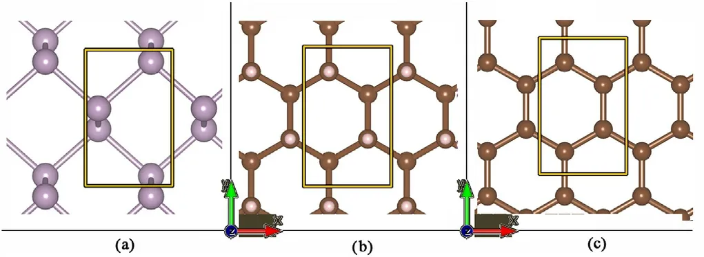
Fig.1. Unit cells(Yellow rectangle)used for(a)Phosphorene.(b)Graphane.(c)Graphene. (Not to scale.)
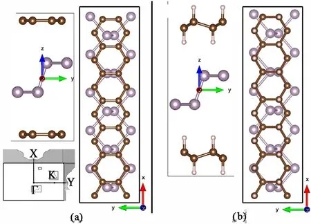
Fig. 2. (a) Relaxed van der Waals heterostructure of G/P/G. Side view shows the 2 planar sheets covering the phosphorene layer. (b) Relaxed van der Waals heteostructure of GRA/P/GRA. Both structures were calculated with phosphorene sized lattice parameters.
The basic, relaxed, stacked principal layers forming G/P/G and of GRA/P/GRA are shown in Fig.2
To study the band structures and the effects of electric field in vdW devices, we calculated the band structures of our fully periodic vdW heterostructures and applied a constant electric field in direction normal to the plane,simulated through a saw-like potential which goes to zero in vacuum,with our structure in the center.The charge densities for every case were calculated without atom relocation of the relaxed structure without electric field.
For the graphene/phosphorene/graphene heterostructure we changed the field between 0 and 11 V/nm as seen in Figs.3 and 4.
The bandgap of the relax structure under no electric field is 2.06 eV,and through projected density of states(PDOS)analysis,we can see that it is due to the bandgap in the phosphorene layer, the computed wide band gap of graphane(9.8 eV) causes the carbon state to be completely absent from the energy levels in the valence band close to the band gap,but at the same time due to the position of this Fermi level in graphane,we can see that in the conduction band carbon states are close to 1 eV from the lowest unoccupied energy states.
We also note that DFTB calculations of phosphorene band structures point to a bandgap or 2.6 eV in pure phosphorene, meaning that interactionswithgraphanelayers,probablydue to theclosenessto hydrogen atoms,reduce the effective bandgap in the central P layer.This may have consequences in transport when going from G/P/G or pure P,where the bandgap is mostly unchanged,to sites with GRA/P/GRA structures.
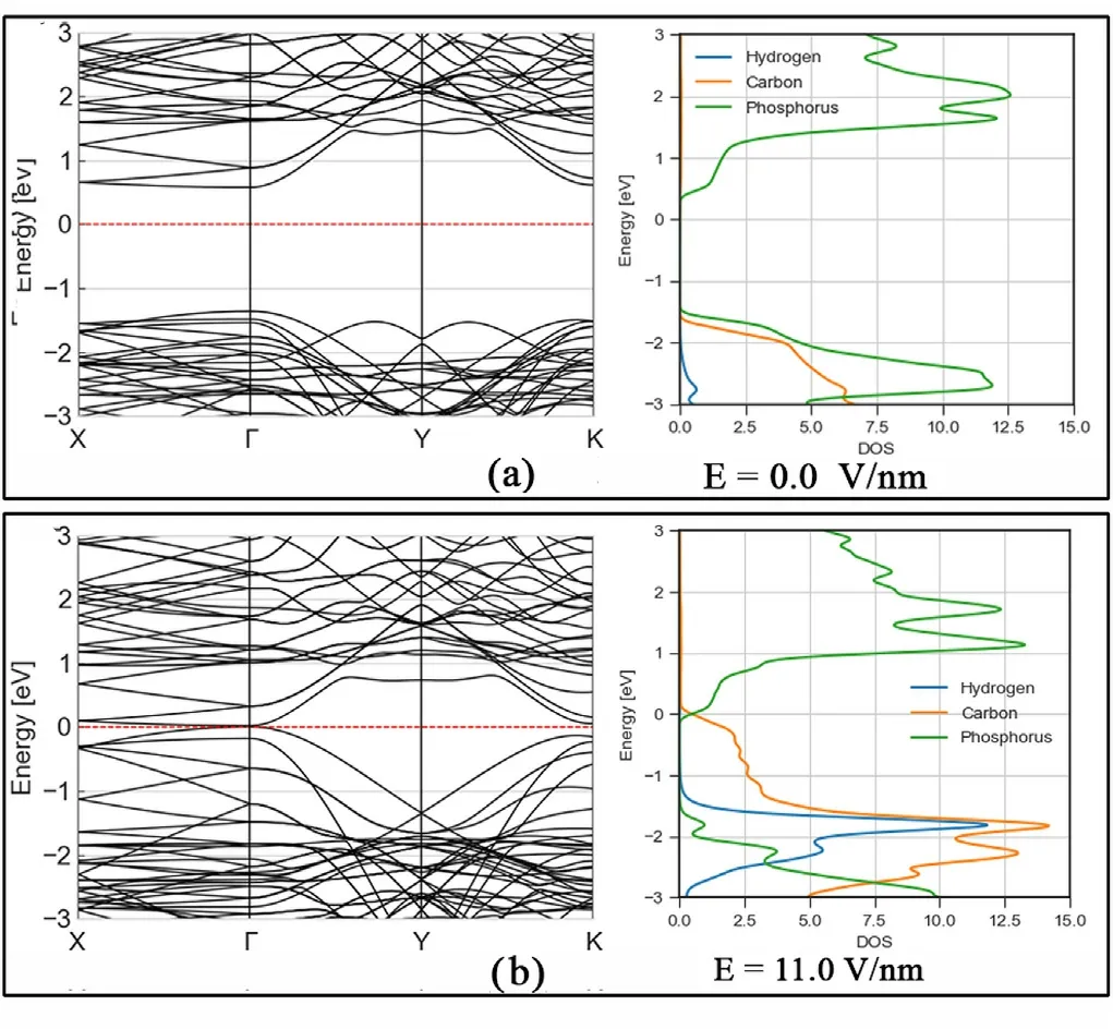
Fig. 3. (a) Band structure and PDOS of relaxed GRA/P/GRA van der Waals heterostructure. A bandgap of 2 eV is observed, due to Phosphorene bands. (b)Band structure and PDOS of GRA/P/GRA under 11.0 V/nm of electric field normal to the plane. The bands show that the Schottky barrier between carbon and phosphorus states has now been reduced to 0 eV.

Fig. 4. Energy gap in band structure of GRA/P/GRA vdW heterostructure.Below 0.5 V/nm the smaller gap corresponds to phosphorene, above the gap is reduced due to shift in the carbon states towards the fermi level.
In Fig. 4 two field magnitudes are notable: first, after 0.5 V/nm, the Schottky barrier between conduction band graphene states and valence band phosphorene states is the same as the bandgap in our phosphorene layer.Thus,no change in the gap is observed even though a shift in the energy levels still occurs for the carbon states. The second important change is at 11 V/nm, where we can see our Schottky barrier going to 0 eV.For the GRA/P/GRA structures the relative shift caused by electric field is again observed between carbon and phosphorene states, mainly through carbon valence and conduction bands getting closer to the Fermi level outside of the Dirac cones.In Fig.5 we can see that at zero field the band structure is mostly an overlap of phosphorene and graphene bands,with slightly shifted Dirac cones,due to the strain in the graphene layer.At 9.0 V/nm there is a visible shift towards the Fermi level in some carbon bands where, taking the gap at the Gamma point as a reference,we can see the field closed this distance from 1.10 eV to 0.02 eV.The PDOS shows how from the typical semi-metallic graphene DOS we go to a metallic behaviour with uniform DOS around the Fermi level. It is notable too that the gap between phosphorus related energy states being maintained around the 2.0 eV at all times.
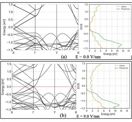
Fig. 5. (a) Band structure and PDOS of relaxed G/P/G van der Waals heterostructure. Conduction band is dominated by carbon states, while some phosphorus-carbon coupling exists in the valence band. (b) Band structure and PDOS of G/P/G under 9.0 V/nm of electric field normal to the plane.Graphene behaviour becomes metallic due to shift of conduction and valence band towards the Fermi level, while phosphorene appear unchanged.
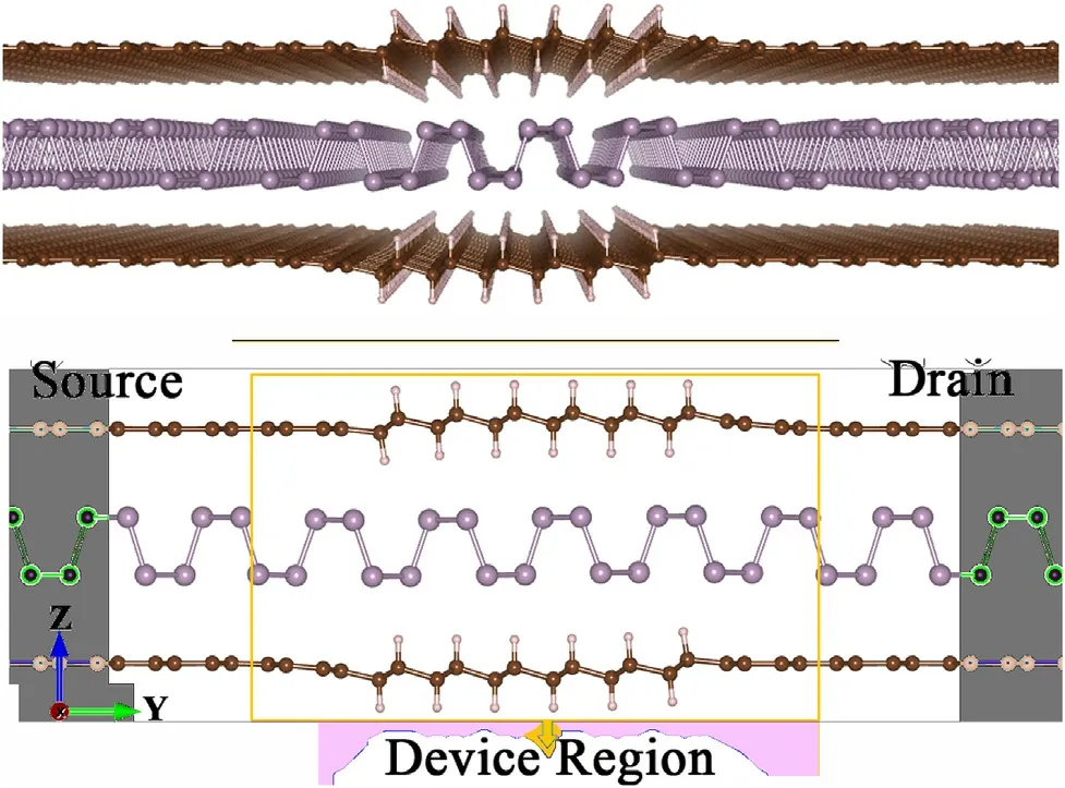
Fig.6. Graphene,hydrogenated graphene(graphane)and phosphorene van der Waals field effect device. The calculated device extends infinitely in the x axis,while the contacts extend infinitely in the plane as pure vdW graphene/phosphorene/graphene structures.
Further exploration into the band structure reveals coupling of phosphorus and carbon states in both the Dirac cones and bands near the Fermi level around the Gamma point. Since both of these areas are actually affected by the field, and show clear shifts, we determine that this small amount of phosphorus-related energy states do actually shift with this field in the same way carbon states do.These shifts have been reported before as stronger effects in bi-layer graphene/phosphorene vdW structures[33].
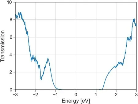
Fig. 7. Transmission spectrum of G/GRA/P van der Waals Field Effect Device.The calculated device extends infinitely in the x axis, while the contacts extend infinitely in the plane as pure vdW G/P/G structures.
3.2. Field effect device
The complete device region was formed based on 5 principal layers of graphene/phosphorene/graphene along the Y axis (see Fig. 6, and infinite in the x axis, where the middle layers had their carbon atoms hydrogenated, while the 2 outer PLs are pristine.The relaxed full structures are different from simple juxtaposing of our GRA/P/GRA with G/P/G vdW structures.For relaxation calculations these layers were put next to G/P/G leads and the structure was relaxed.
As shown in Fig. 6 the full device region has a channel length of 22.5 Å,while the hydrogenated part of the protective graphene sheets is in the order of 13.5 Å. The vertical spacing among the structures in the device is closer to typical G/P/G van der Waals distances than to the ones seen for GRA/P/GRA. This may cause more interaction of phosphorus with hydrogen atoms,although no structural change is seen in the central phosphorene structure with respect to an ideal, isolated phosphorene layer.
The transmission spectrum of the device under no bias or gate effects,as shown in Fig. 7, presents the expected bandgap seen in both vdW structures that compose the system, and transmission outside at higher and lower energy states. The Local Density of States (LDOS) plot shows that valence band states are mostly related to phosphorus, a more complex case occurs over the conduction band, where below Ec+ 0.5eV we can see phosphorus states, but over this level both carbon and phosphorus are present.
3.3. Outlook: modification of phosphorene channel
The graphene/lateral heterostructure layers could provide the phosphorene channel more control over quality and doping during device fabrication in experimental settings. Since it is also clear from the electronic transmission analysis, Fig. 7, that conduction through the device above Ev+0.5eV is dominated by phosphorene behaviour,then a natural derivation of the basic structure would be to try to manipulate in detail the doping of the phosphorene layer before the integration into the device. To determine the effects of such modifications we explored phosphorene doping of common phosphorene adatoms,particularly focusing on defect densities that enabled changes on the transport behaviour inside the bandgap for extremely short channels(<5 nm).
Since atmospheric conditions typically have phosphorene reacting to Oxygen [14,34], this was selected as the first important dopant to analyse,the second dopant simulated was Sulfur[35,36],the next chalcogen in the periodic table,and thus a common dopant for phosphorene.
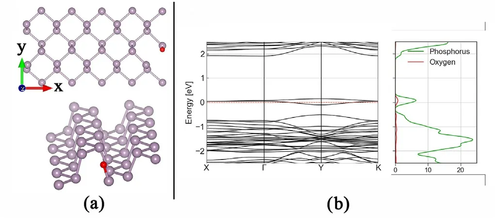
Fig. 8. (a) Molecular structure of oxygen substitutional atom defect in phosphorene periodic structure of 5 × 2 basic unit cells of phosphorene. (b) Corresponding band structure,presenting emerging energy levels inside the bandgap,with visible dispersion.
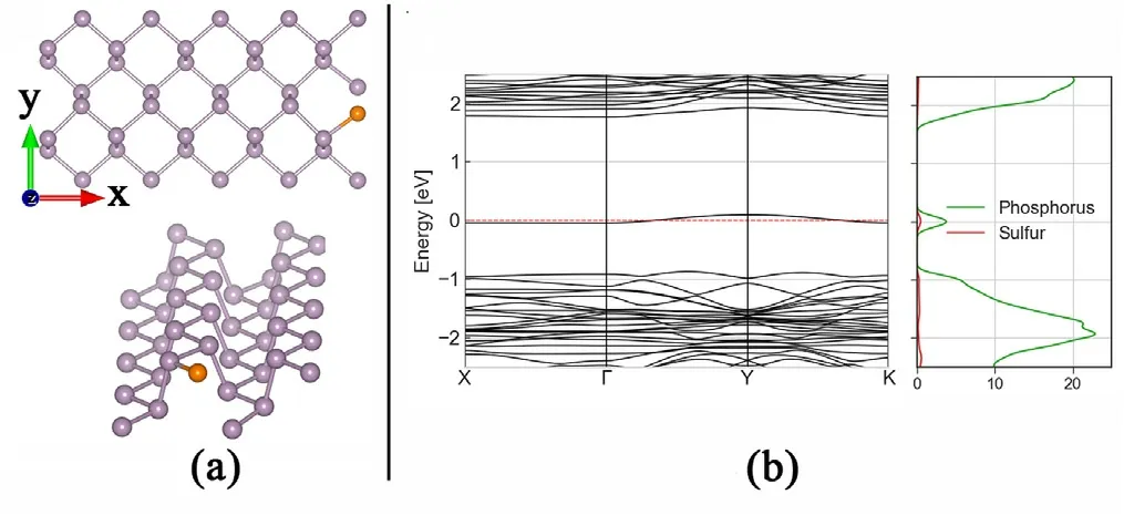
Fig. 9. Molecular structure of sulfur substitutional atom defect in phosphorene periodic structure of 5 × 2 basic unit cells of phosphorene. (b) Corresponding band structure, presenting emerging energy levels inside the bandgap, with visible dispersion.
In Figures A12 and A13 we can see different relaxed structures with different densities of Oxygen and Sulfur defects, respectively, as both adatom and substitutional atoms. Aside from distortions in the conduction and valence bands,the main visible effect is the emergence of energy levels inside the gap of phosphorene, one unfilled state close to the conduction band and one filled states effectively reducing the bandgap.The effects of increased density (Figs. 8 and 9) in a certain direction generates dispersion in these levels enabling half filled bands, thus changing the semiconducting behaviour of phosphorene around the Fermi level, and having consequences in the transmission spectrum, as can be seen in Figs.10 and 11.
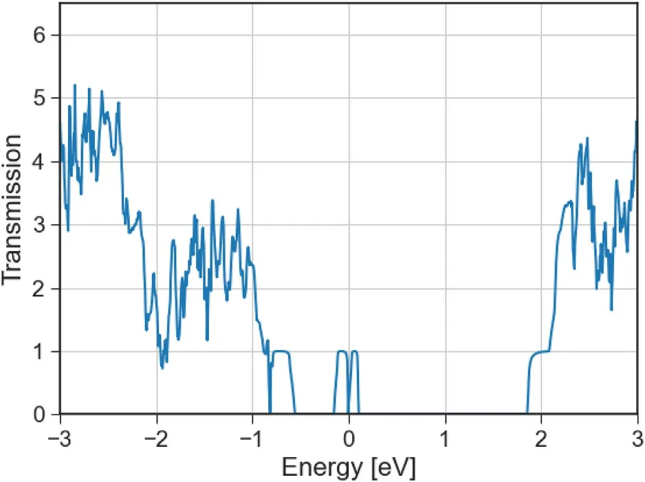
Fig. 10. Electronic transmission spectrum of phosphorene with high density oxygen substitutional atoms in the transport(armchair)direction.The principal layers for transport involve 5 × 2 unit cells of phosphorene, with one Oxygen substitutional atom in each PL (See Figure A12f).
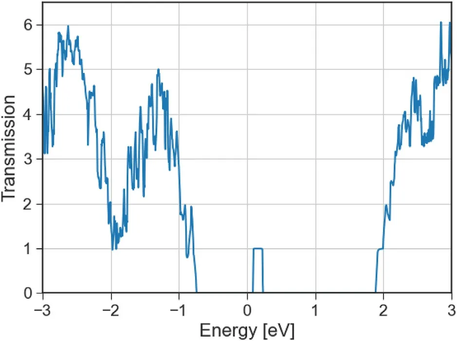
Fig. 11. Electronic transmission spectrum of phosphorene with high density sulfur substitutional atoms in the transport (armchair) direction. The principal layers for transport involve 5 × 2 unit cells of phosphorene, with one Oxygen substitutional atom in each PL (See Figure A13f).
The electronic transmission spectrum of high density Oxygen substitutional atoms shows that conduction is now enabled inside the phosphorene bandgap, in electronic states related to the defects which for these high densities are now delocalized in space. A similar effect is seen for the Sulfur equivalent,but here the width of the energy range in which transmission is possible is narrower,being more sensitive to small biases.Devices with fully doped channel,source and drain,present high sensitivity to bias,having specific ranges in which conduction is enabled by the high defect density.
4. Conclusion
We have studied electric field effects in van der Waals heterostructures of phosphorene layered in between graphene or graphane sheets, observing shifts in the carbon and phosphorus bands. Lower phosphorene/graphane Schottky barriers under higher electric fields are observed,while increased metallic behaviour of graphene and increased phosphorus states near the Fermi level are observed for the graphene/phosphorene/graphene structures.
We combine both vdW structures into a lateral heterostructure, in which graphene layers work as contacts and protective layers of a phosphorene channel layer, and are separated by an hydrogenated(graphane-like) band which could work as a gate insulator obtaining a basic phosphorene field effect device. The simulated device maintains electronic transmission properties of phosphorene, while being capable of protecting phosphorene from degradation in non-vacuum settings.At the same time the planar geometry of a lateral graphene-graphane heterostructure ensures minimal vertical size.
We also analysed doping and defect-enabled electronic transport in phosphorene channel layers.We see mainly distortions from Oxygen and Sulfur adatoms,and new energy levels appearing inside the bandgap for substitutional atoms.Notably,a new filled level appears for Sulfur,while a filled and a closed unfilled level emerge for Oxygen substitutional defects. We determine the effects of defect density in the transport direction, which enables electronic conduction inside the phosphorene bandgap through narrow energetic ranges around the Fermi level.
Declaration of competing interest
No conflicting interest is declared.
Acknowledgements
The authors thank T.Radchenko,I.Sahalianov,and V.Tatarenko for useful discussions. This investigation has been supported through the German Research Foundation within the project “Straintronics of imperfect quasi-two-dimensional materials: coplanar vs lamellar heterostructures” (CU 44/43). We acknowledge the Center for Information Services and High Performance Computing (ZIH) at TU Dresden for providing computational resources.
Appendix A. Detailed geometry and band structure calculations with defects
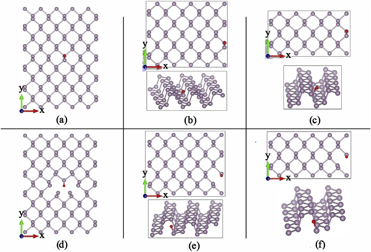
Fig.A.12. Molecular structures of periodic phosphorene defects.(a),(b)and(c)are adsorbed Oxygen atoms(red)in periodic structures of 5×5,5×3 and 5×2 basic unit cells of phosphorene. In (d), (e) and (f) an Oxygen atom substitutes one phosphorene atom in periodic structures of 5 × 5, 5 × 3 and 5 × 2 basic unit cells of phosphorene.
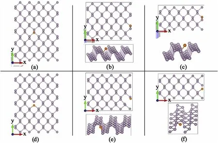
Fig.A.13. Molecular structures of periodic phosphorene defects.(a),(b)and(c)are adsorbed Sulfur atoms(orange)in periodic structures of 5×5,5×3 and 5×2 basic unit cells of phosphorene.In(d),(e)and(f)a Sulfur atom substitutes one phosphorene atom in periodic structures of 5×5,5×3 and 5×2 basic unit cells of phosphorene.

Fig.A.14. Band structures and PDOS of periodic phosphorene defects.(a),(b)and(c)are adsorbed Oxygen atoms in periodic structures of 5×5,5×3 and 5×2 basic unit cells of phosphorene.Distortion in the phosphorene band is visible with new spatially localized energy states close to the conduction band.In(d),(e)and(f)an Oxygen atom substitutes one phosphorene atom in periodic structures of 5 × 5, 5 × 3 and 5 × 2 basic unit cells of phosphorene (See Figure A12). Aside from distortions new filled and unfilled energy states appear in the middle of the bandgap, spatially localized for (a), but with enough dispersion to provide metallic behaviour for (c).
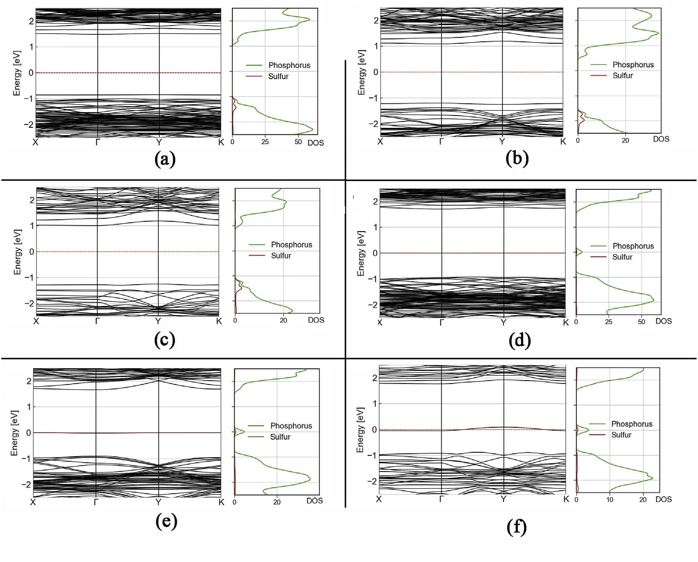
Fig.A.15. Band structures and PDOS of periodic phosphorene defects.(a),(b)and(c)are adsorbed Sulfer atoms in periodic structures of 5×5,5×3 and 5×2 basic unit cells of phosphorene. In (d), (e) and (f) an Sulfer atom substitutes one phosphorene atom in periodic structures of 5 × 5, 5 × 3 and 5 × 2 basic unit cells of phosphorene. (See Figure A13). A new spatially localized filled energy state appears at in the middle of the bandgap win (d), dispersion increases with increased density with the level becoming half filled for (e) and (f).
- Namo Materials Science的其它文章
- Recent advances in graphene and other 2D materials
- Editorial for a special issue on graphene and 2D alternative materials: From preparation to potential applications
- Biaxial versus uniaxial strain tuning of single-layer MoS2
- Room temperature synthesis of two-dimensional multilayer magnets based on α-CoII layered hydroxides
- Electrostatic interactions in twisted bilayer graphene
- The effect of rippling on the mechanical properties of graphene