基于二氧化钒宽、窄带可切换的双功能超材料吸收器研究
封覃银,裘国华 ,严德贤 ,李吉宁,李向军
(1.中国计量大学 信息工程学院 浙江省电磁波信息技术与计量检测重点实验室,杭州 310018;2.天津大学 精密仪器与光电子工程学院,天津 300072)
1 Introduction
Terahertz wave (THz wave) mainly refers to electromagnetic wave with frequency between 0.1 THz and 10 THz, which is located between microwave and infrared light wave[1].In recent years,with the rapid development of terahertz detection technology and time-domain spectroscopy technology, terahertz wave detection, modulation and other related technologies have attracted more and more attention[2].Metamaterials are a new type of artificially designed electromagnetic composites that have attracted great interest in many potential applications, such as terahertz absorbers[3-4], polarization converters[5], sensors[6].In recent years, many researchers have proposed a variety of the terahertzbased metamaterial absorber models, and studied their single frequency band[7], multi-frequency band[8-10]and wide frequency band[11-12]characteristics.As a functional device that can achieve high absorptivity of incident electromagnetic wave[13-14],metamaterial absorber has promising application prospects[18-19]in many fields such as infrared detection[15], modern communication, electromagnetic stealth[16], thermal radiation, and sensing[17].The early terahertz absorber has a single resonance mode and narrow absorption spectrum bandwidth.Most designed metamaterial absorption devices can only achieve a single function at the working frequency or cannot tune the absorption performance according to the application requirements.Various shortcomings limit its practical application.
With the emergence of functional materials(phase change materials) such as graphene[20-21], liquid crystals (LC)[22], and vanadium dioxide (VO2)[23],it is possible to change the properties of materials simply by applying excitations such as electricity[24-25], magnetism, light[26], and temperature[27].Combining these functional materials with metamaterial structures allows multiple functions to be implemented in a single metamaterial device, thus driving the rapid development of terahertz metamaterial absorbers.VO2, as an excellent phase change material, has optical and electrical properties that change significantly during the phase change, and the conductivity can change by 4-5 orders of magnitude[23], making it ideal for tunable multifunctional metamaterial device.Liu[23]et al.proposed a VO2-based ultra-wideband absorber that can achieve modulation of 5% to 80% absorption in the wideband range of 1.2 to 3.2 THz.Song[28]et al.proposed the design of a VO2-based terahertz wideband tunable absorber, by which the amplitude of the wide-band absorption band can be adjusted from 5% to 96% when the VO2conductivity changes from 10 S/m to 2000 S/m.Zhang[29]et al.proposed a terahertz bi-functional absorber with wide-band and narrow-band absorption characteristics based on a graphene/spacer-VO2/spacer-metal structure.The operating bandwidth and intensity of narrow-band absorption and wide-band absorption can be dynamically tuned by changing the Fermi level of graphene.Huang[30]et al.proposed a tunable wideband terahertz absorber, by which the absorption can be dynamically tuned from 4% to 100% by varying the conductivity of VO2, achieving nearperfect amplitude modulation.
Based on the phase change characteristics of VO2, a bi-functional metamaterial absorber with switchable wide-band and narrow-band absorption is proposed in this paper, and the wide-band and narrow-band absorption characteristics of this absorber can be tuned by changing the conductivity of VO2.When VO2is in the metallic state, the structure is a wide-band absorber consisting of the top layer formed by the metal split ring resonator and VO2disc, the upper polyimide (PI) dielectric layer,and the VO2film.When VO2is in an insulating state, the structure is mainly a narrow-band absorber consisting of the top layer formed by the metal split ring resonator and VO2disc, the upper PI dielectric layer, the VO2film, the lower PI dielectric layer, and the metal substrate.Due to the high symmetry of the designed cell structure, the absorber also has the characteristics of insensitivity in polarization and incidence angles over a wide-range,which greatly reduces the limitations of the absorber in the practical application process.The wide- and narrow-band switchable bi-functional absorber proposed in this paper can provide new research ideas for multifunctional tunable devices in terahertz and other frequency bands.
2 Structure and methodology
The cell structure of the terahertz metamaterial absorber[28-32]is shown in Figure 1 (Color online),which shows the three-dimensional structure, top view and side view of the periodic cell of the absorber, respectively.The cell structure from top to bottom is a top pattern consisting of a metal split ring resonator and VO2disc, an upper PI dielectric layer, a VO2thin film, a lower PI dielectric layer,and a metal substrate, and the device structure is symmetric about thexandyaxes.The resonant structure of the absorber is composed of a metal split ring resonator and a VO2disc placed in the center.The calculated optimal geometrical parameters are the period of the structural cellPx=Py=80 μm, the ring opening angleα=30°, the outer radius of the split ringR1=64 μm, the width of the ringW=2 μm, the radius of the VO2discR2=47 μm, the relative permittivity of the upper PI dielectric layerε=2.0, the loss angle tangent tanδ=0.02[33], and the thicknessZ3=18 μm, the thickness of the VO2filmZ=1.5 μm, and the thickness of the lower PI dielectricZ1=45 μm.And the metal substrate of the ground plane is a gold material with a thickness ofZ=1 μm and a conductivity ofσ(gold)=4.09×10⁷S/m[33].
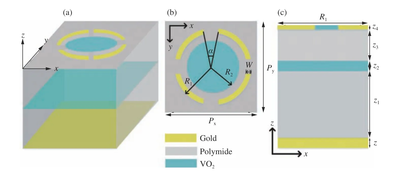
Fig.1 The absorber (a) 3D schematic; (b) top view; (c) side view图1 (a)吸收器三维示意图;(b)顶部视图;(c)侧视图
In this paper, the absorption characteristics of the designed switchable metamaterial absorber are numerically simulated by CST software.Terahertz waves are incident on the absorber along -zdirection perpendicular to the absorber surface, and the electric field of the incident wave is polarized alongxdirection and the magnetic field is polarized alongydirection.The periodic boundary conditions are used inxandydirections, and the open boundary condition is used in thezdirection.The Drude mod-is used to describe the optical properties of VO2in the terahertz frequency range, where ε∞=12 is the high-frequency relative permittivity,ωp(σ) is the plasma frequency with respect to the conductivity,σis the conductivity of VO2, γ = 5.75 × 10¹³rad/s is the collision frequency,and bothωp(σ) andσare proportional to the free carrier density.The relationship between the plasma frequency and conductivity of VO2can be approximated as, whereσ= 3×10⁵S/m,rad/s.By applying the excitation of external electric field, optical field, or temperature field, the phase transition process of VO2can occur in a short time.The variation range of conductivity before and after the phase change of VO2is about 200 S/m~2×105S/m.By changing the conductivity of VO2, the wide-band and narrow-band absorption functions of the absorber can be switched.When VO2is in the metallic (or insulating)state, its conductivity is 2×10⁵S/m (or 200 S/m)[30],and these two conditions are used to simulate the phase change process of VO2in the paper.In the practice, the phase change process of VO2can be achieved by changing the temperature.Under thermally excited conditions, the phase transition temperature of VO2is approximately 68 ℃.At room temperature, VO2is in the insulating state;when the temperature is heated from low to high temperature (over 68 ℃), the molecular structure of VO2changes and VO2converts from the insulating state to the metallic state; the process is reversible and VO2converts from the metallic state to the insulating state when the temperature decreases from the phase change temperature (68 ℃).
3 Results and discussion
The designed metamaterial bi-functional absorber is simulated by using the commercial electromagnetic analysis software CST Microwave Studio.The reflection coefficient (S11) and transmission coefficient (S21) of this absorber are obtained through simulation, then the electromagnetic absorption rate (A) of this structure can be calculated from the following equation:

whereR=|S11|2andT=|S21|2are the reflectance and transmittance obtained from the frequency-dependentS-parameters, and the reflectionR⊥of the crosspolarized wave is also discussed here.In the studied terahertz frequency range, the transmission (T) of the overall metamaterial structure is always 0 due to the presence of metal plates or metallic VO2films at the bottom in both states, and the thickness of the metal plates or VO2films is much larger than the skin depth of the electromagnetic waves, thus suppressing the transmission.The reflection and absorption spectra of VO2with different conductivities are shown in Fig.2(a) and Fig.2(b).When the conductivity changes from 200 S/m to 2×10⁵S/m,the corresponding absorption changes from narrowband absorption to wide-band absorption, achieving a perfect switch between wide and narrow-band absorption functions.

Fig.2 (a) Reflection spectrum; (b) absorption spectrum; (c) real part of and (d) imaginary part of the relative impedance with different conductivities of VO2图2 二氧化钒不同电导率时的(a)反射光谱;(b)吸收光谱;(c)相对阻抗的实部和(d)虚部
When terahertz wave is incident perpendicular to the device surface, we introduce impedance matching theory to elucidate the intrinsic mechanism for the absorber's changes.Both the real and imaginary parts of the relative impedance of the absorber can be derived from theS-parameter inversion method.The absorption rate and relative impedance can be expressed as[34-35]:
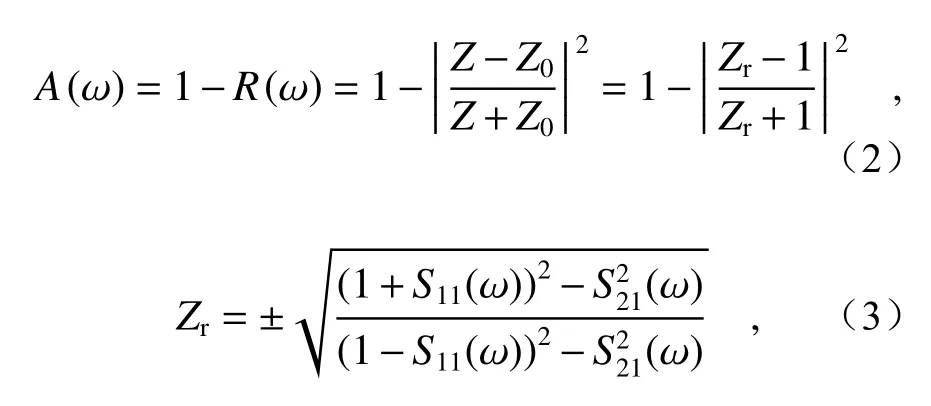
where Z0and Z are the effective impedances of the free space and the absorber, respectively.AndZr=Z/Z0is the relative impedance between the absorber and the free space.The absorption of the wide-band absorber reaches the maximum when the impedance of the absorber matches the impedance of the free space, i.e., the relative impedance of the structureZr=1.The variation of the real and imaginary parts of the relative impedance for different VO2conductivities is shown in Fig.2 (c) and (d).Obviously, with the continuous increase of the conductivity, the real part gradually approaches to 1 while the imaginary part gradually approaches to 0 in the range of 1.34~2.25 THz, which means that the effective impedance of the absorber and the free space gradually match each other.When VO2is in the metallic state, i.e.,σ(VO2) = 2×10⁵S/m, the designed structure obtains the highest absorption rate and the widest absorption bandwidth at the same time.
3.1 Metamaterials can be used as wide-band absorbers when VO2 is in the metallic state
When VO2is in metallic state, the designed switchable metamaterial can be used as a wide-band absorber, which consists of a metal split ring resonator on top embedded in a VO2disc, an upper PI medium, and a VO2film.When the VO2is in the metallic state, the bottom metallic phase VO2acts as the reflection layer, which can prevent the occurrence of transmission.The structural parameters are shown in Fig.1, and the absorber model is simulated by the finite element method, applying the cell boundary conditions to thexandyboundary conditions and the open boundary inzdirection, with the terahertz wave incident along -zdirection.The reflection and absorption spectra, as well as the real and imaginary parts of the relative impedance of the wide-band absorber are given in Figure 3 (Color online) when the conductivity of VO2is 2×10⁵S/m(metallic state), whereA(ω) denotes the absorption spectrum,R(ω) denotes the reflection spectrum, and Re(Zr) and Im(Zr) represent the real and imaginary parts of the relative impedance of the wide-band absorber, respectively.Two different absorption peaks can be observed at 1.53 THz and 2.12 THz, and the designed structure can absorb more than 90% of the energy in the frequency range from 1.34 to 2.25 THz with a bandwidth ratio (fmax-fmin)/[(fmax-fmin)/2][37]of 50%.And the absorption in the frequency range from 1.10 to 3.18 THz is greater than 50%, and the corresponding bandwidth ratio is 97%.As shown in Fig.1(a), the introduction of the top VO2disc changes the effective impedance of the structure,and the incident electromagnetic waves are better matched with the free space, which also enhances the overall absorption performance of the structure.Therefore, in the wide frequency range of 1.53~2.12 THz, the designed wide-band absorber achieves impedance matching with the free space and obtains a better absorption and wider bandwidth.
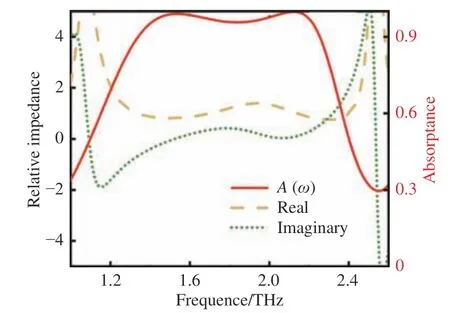
Fig.3 Reflection and absorption spectra, real part and imaginary part of relative impedance when the conductivity of vanadium dioxide is 2×10⁵ S/m图3 二氧化钒电导率为2×10⁵ S/m时反射和吸收光谱、相对阻抗的实部、虚部
In general, the geometric parameters of the structure have an influence on its resonant frequency and absorption rate.Also, errors can be introduced in the structural dimensional parameters during the device processing.Therefore, the structural parameters of the device were investigated.The variation of the terahertz absorption spectrum of the device with the geometric parameters (α,Z3,R2) was studied under the condition that the other parameters were kept constant as initial settings, and the results are shown in the following figures.From Fig.4(a), it can be seen that the absorption bandwidth increases with the increase of the opening angleα.The center frequency of 1.84 THz shows a slight blue-shift trend with the increase ofα.The resonance peak at the frequency of 1.53 THz remains basically unchanged, and the resonance peak at the frequency of 2.12 THz shows a blue-shift trend, therefore, the absorption bandwidth increases and the absorption rate decreases with the increase of the opening angleα.In Fig.4(b), the intensity of the absorption peak first decreases slightly with the increase ofZ3and reaches the optimum absorption at 18μm, and then the absorption decreases with the increase ofZ3.In Fig.4(c), the absorption bandwidth changes less with the increase of the radiusR2of VO2disc, and the absorption rate decreases slightly, and the best absorption rate is obtained at 47 μm, and the absorption curve shows a blue-shift trend when the radius increases from 44 μm to 47 μm.In summary, it can be seen that the effect of the change in the opening angle on the absorption bandwidth is more significant than that of the dielectric layer thickness and the radius of the VO2disc.

Fig.4 The influence of the structural parameters of the absorber cell: (a) the opening angle α; (b) the thickness of the upper PI medium Z3 and (c) the radius of the VO2 disk R2, on the terahertz absorptivity at the conductivity of 2×10⁵ S/m图4 当电导率为2×10⁵ S/m时,吸收器单元结构参数对太赫兹吸收率的影响。(a)开口角度α;(b)上层PI介质厚度z3;(c) VO2圆盘半径R2
To further understand the operating mechanism of the wide-band absorber in detail, we have studied the electric field distribution at the two resonant frequencies of the wide-band absorber,1.53 THz and 2.12 THz, as shown in Figure 5.Figure 5 gives the electric field distribution of the absorber at 1.53 THz and 2.12 THz when the incident terahertz wave is transverse electric (TE) polarized, from which it can be seen that the electric fields at the two frequency points are mainly distributed at the two ends of the opening of the metal split ring resonator, the VO2disc near the opening of the metal ring and alongy-direction; and the electric field intensity at the frequency of 2.21 THz is more concentrated compared with the induced electric field intensity at the frequency of 1.53 THz.In addition, the electric field intensity is gradually weakened along the inner edge of the VO2disc parallel tox-axis and near the opening of the metal ring, which may be caused by the weak dipole resonance of the VO2disc in parallel tox-axis near the opening of the metal ring.Due to the structural symmetry, the results of the electric field distribution of the wideband absorber at the above two frequency points exhibit an overall 90° rotation when the incident wave is TM-polarized.
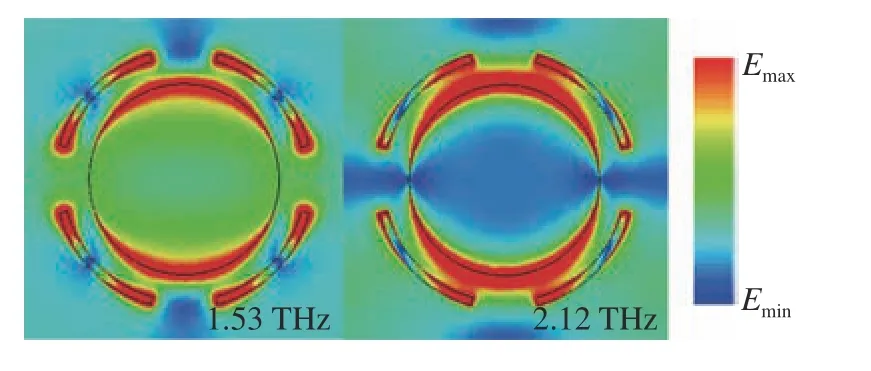
Fig.5 Electric field intensity distribution at the two absorption peak frequencies of 1.53 THz and 2.12 THz under TE mode图5 1.53 THz、2.12 THz在TE极化下两个吸收峰频率处的电场强度分布
For the needs of absorbers in practical applications, polarization angle insensitivity and incidence angle insensitivity are two very important characteristics.Figure 6(a) (Color online) shows the variation of the absorption performance of the metamaterial absorber with the incident terahertz wave frequency and the incident angle in the TE mode.According to the calculated results, the designed absorber still exhibits a stable absorption rate and a wide operating bandwidth in the large incident angle range of 0°~60°, leading to a high incident angle tolerance.When the incidence angle is larger than 60°,the main absorption peak becomes narrower as the incidence angle increases.Therefore, the absorber can still provide good absorption characteristics even at larger incidence angles.In addition, for TM polarization, the absorption performance remains stable up to 8° as shown in Fig.6(b) (Color online).When the incidence angle is larger than 8°, the absorption bandwidth becomes narrower and some higher order modes appear.A similar dependence of the absorption spectrum on the incidence angle was observed in the previously reported VO2-based absorber[36].Therefore, the absorption performance of TE polarization is superior to that of TM polarization.The effect of the polarization characteristics of the incident terahertz wave on the absorption performance was also investigated.Figure 6(c) (Color online) shows the absorption rate vs.frequency as the polarization angle varies from 0° to 90° when a terahertz wave is incident vertically on the absorber surface.It can be seen from Fig.6(c) that the absorption curves of this wide-band absorber are highly overlapping, i.e., the absorption rate of the absorber is completely independent of the polarization under normal incidence conditions, which is highly related to the symmetry of the absorber cell structure inxandydirections, and the large incidence angle and polarization insensitivity characteristics show high potential for applications in energy harvesting and optical sensing.

Fig.6 (a) The absorption of the wide-band absorber with TE polarization at different incident angles; (b) the absorption of the wide-band absorber with TM polarization at different incident angles; (c) the absorption spectrum of the wide-band absorber with different polarization angles; at the conductivity of 2×10⁵ S/m图6 当电导率为2×10⁵ S/m时(a)不同入射角度时,TE极化的宽带吸收器的吸收率;(b)不同入射角度时,TM极化的宽带吸收器的吸收率;(c)不同极化角时宽带吸收器的吸收光谱图
3.2 Metamaterials can be used as narrow-band absorbers when VO2 is in the insulated state
When VO2is in the insulating state, the structure of a multi-band absorber consists of a metal split ring resonator on top embedded in a VO2disc,an upper PI dielectric, a VO2film, a lower PI dielectric, and a metal substrate.The simulation study is performed by using the numerical simulation method of electromagnetic field, and the three-peak absorption spectrum of the multiband absorber can be achieved.Figure 7 shows the reflection and absorption spectra as well as the real and imaginary parts of the relative impedance of the narrow-band absorber at a VO2conductivity of 200 S/m.Three absorption peaks exist in the frequency range from 2.4 THz to 4 THz with the resonance frequencies of 2.54 THz, 2.93 THz, and 3.34 THz, the corresponding absorption of 96%, 99.9%, and 99.3%, and the corresponding Full Width at Half Maximum(FWHM)[37]of 93.6 GHz, 206.7 GHz, and 39 GHz,respectively, achieving overall perfect multiband absorption.It can also be seen from Fig.7 that the real part of the impedance gradually approaches to 1 and the imaginary part gradually approaches to 0 near the multiband absorption peak.The designed multiband narrow-band absorbers achieve the impedance matching between the narrow-band absorber and the free space near the resonant frequencies of 2.54 THz, 2.93 THz, and 3.34 THz.
Under the condition that other parameters remain unchanged as initial settings, the effect of the geometric parameters (α,Z1,W) on the absorption rate was studied, and the calculated results are shown in Figure 8.In Fig.8(a), the absorption intensity increases significantly with the increase of the opening angle (α), which has a significant effect on the absorption rate at the resonance frequency of 2.54 THz; the absorption rate decreases gradually with the increase of the opening angle at the resonance frequency of 2.93 THz, while the absorption intensity remains unchanged at the resonance frequency of 3.34 THz.In Fig.8(b), the thickness of the lower PI medium (Z1) increases from 44 μm to 48 μm in steps of 1 μm, which has a significant effect on the absorption peaks at 2.93 THz and 3.34 THz, and the absorption rate decreases.The strongest absorption intensity is achieved whenZ1is 45 μm, after which the overall absorption intensity decreases slightly with the increase ofZ1.In Fig.8(c), the intensity of the absorption peak first increases with the width of the metal split-ring (W),and the absorption peak in the middle frequence band is more affected, and the strongest absorption peak is obtained atW=2 μm, after which the overall absorption intensity decreases with the increase ofW.In summary, it can be seen that the effect of the opening angle is more significant than that of the dielectric layer thickness and the width of the metal split-ring on the absorption bandwith.
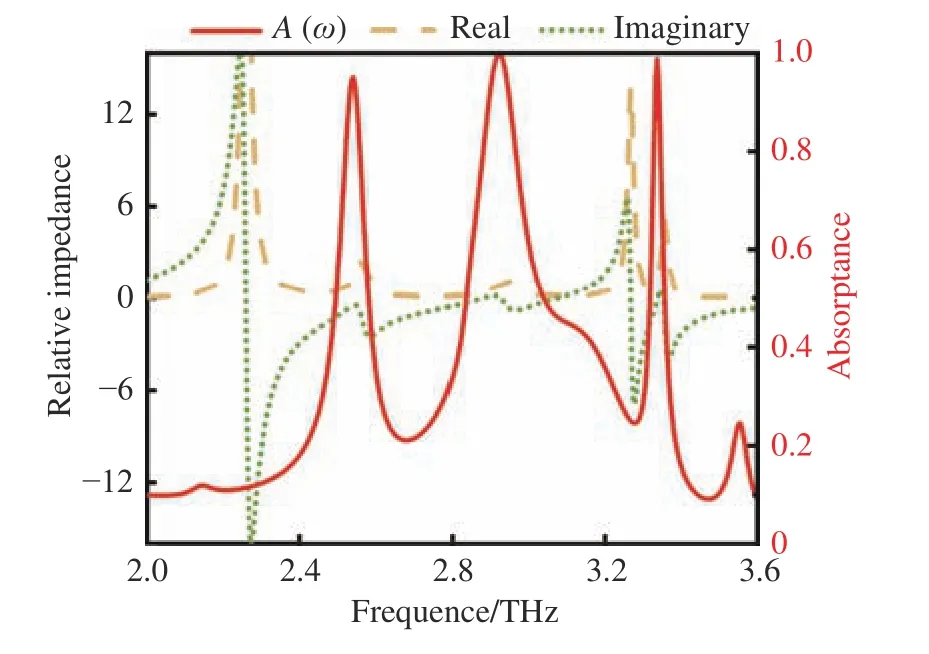
Fig.7 Reflection and absorption spectra, real part and imaginary part of relative impedance when the conductivity of vanadium dioxide is 200 S/m图7 二氧化钒电导率为200 S/m时反射和吸收光谱、相对阻抗的实部、虚部

Fig.8 The influence of the structural parameters of the absorber cell: (a) the opening angle; (b) the thickness of the lower PI medium Z1 and (c) the width of the metal split ring resonator W, on the terahertz absorption at the conductivity of 200 S/m.图8 当σ为200 S/m时,吸收器单元结构参数对太赫兹吸收率的影响;(a)开口角度(b)下层PI介质厚度Z1;(c)金属开口谐振环的宽度W而变化
In addition, the electric field intensity distribution at the three absorption peak frequencies of 2.54,2.93 and 3.34 THz under TE mode is shown in Fig.(9).At 2.54 THz, the electric field distribution is highly concentrated along the two openingends of the metal split ring resonator; at 2.93 THz,some energy is uniformly distributed in the center region of the absorber cell; at 3.34 THz, the electric field intensity is strong on both sides of the opening of the metal split ring resonator and within the center region of the absorber cell structure.Due to the symmetry of the structure, the results of the electric field distribution of the narrow-band absorber at the above three frequency points exhibit an overall 90° rotation when the incident wave is TMpolarized.

Fig.9 Electric field intensity distributions at the three absorption peak frequencies of 2.54 THz, 2.93 THz and 3.34 THz under TE mode图9 2.54 THz、2.93 THz和3.34 THzTE极化时三个吸收峰频率的电场强度分布
Next, the absorption characteristics of this multiband metamaterial absorber at different polarization angles were also investigated.Fig.10 depicts the variation of the absorption and frequency when the polarization angle is increased from 0° to 90° in steps of 5°.The results show that the absorption performance of the proposed multiband metamaterial absorber in TE mode does not change with the variation of the incident terahertz wave polarization angle when the terahertz wave is incident vertically on the absorber surface, and its absorption curves are highly coincident.The insensitivity to the polarization angle is related to the symmetry of the absorber cell structure inxandydirections.The intrinsic reason for the symmetry of the designed structure ensures the polarization insensitivity at normal incidence, which is very helpful in many applications.
The structures described in this paper can be processed by molecular beam epitaxy.In 2016, Bianet al.[38]used molecular beam epitaxy to grow VO2films on single-crystal sapphire substrates that can be precisely controlled in thickness.In 2017,Sun Hongjunet al.[39]used molecular beam epitaxy to grow a high-quality stoichiometric VO2films on single-crystal sapphire substrates, and achieved precise control of the film thickness through this technique.For this structure, molecular beam epitaxy can be used to deposit thin VO2films on PI substrates, and then introduce the disc structure to the top of the VO2film.Then, metal microstructures are prepared on PI by the conventional lithography and metallization processes to form metallic split ring resonators.The design method proposed in this study provides a new way to study multifunctional components based on continuous VO2films with completely different functions integrated into one structure.
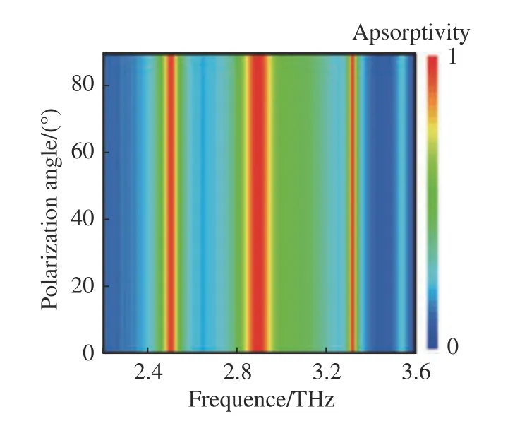
Fig.10 Absorption spectra of narrow-band absorbers with different polarization angles at the conductivity of 200 S/m图10 当电导率为200 S/m,不同极化角时窄带吸收器的吸收光谱图
The terahertz wide-band absorber designed in this paper can be mainly applied to stealth and functional measurements.By absorbing terahertz waves and reducing the energy returned to the detector thus achieving stealth, which can be applied to radar detection, modern warfare weapons and other occasions.The wide-band absorber can be also applied to the field of terahertz wave energy collection and measurement, and the absorber can convert the absorbed energy into electrical energy thus realizing energy measurement.
4 Conclusion
In this paper, a switchable bi-functional metamaterial absorber with wide and narrow bands characteristics is designed, which consists of a top layer pattern composed of a metal split ring resonator and a VO2disc, an upper PI dielectric layer, a VO2thin film, a lower PI dielectric layer and a bottom metal substrate, and can be excited by external electromagnetic fields, optical fields and temperature fields to cause the VO2to undergo an insulating state-metallic state reversible phase transition process, so that the switching between different functions can be realized.The switchable structure is numerically simulated in the frequency range of 0~4 THz by the finite element method.The results show that the structure can achieve the function of a high-performance terahertz wideband absorber with the absorption of 98% in the wide-band frequency range of 1.55 THz to 2.21 THz when VO2is in the metallic state.When VO2is converted from the metallic state to the insulating state, this structure can realize the multi-band narrow-band absorber.The designed metamaterial absorber can achieve narrow-band absorption above 95% at the resonant frequencies of 2.54 THz,2.93 THz, and 3.34 THz.In addition, the effects of geometric parameters on the absorption performance are discussed.The absorber device also shows good absorption performance at large incidence angles due to the polarization insensitivity caused by the symmetric structure.The proposed metamaterial absorber with simple structure, switchable function and perfect absorption can be applied to terahertz optical switches, electromagnetic stealth,modulation, thermal emitters and electromagnetic energy harvesting.
——中文对照版——
1 引 言
太赫兹波(THz波),主要指频率在0.1 THz到10 THz之间的电磁波,位于微波与红外光波之间[1]。近年来,随着太赫兹探测技术以及时域光谱技术的快速发展,太赫兹波的检测和调制等相关技术受到了越来越多的关注[2]。超材料是一种新型人工设计的电磁复合材料,在太赫兹吸收器[3-4]、极化转换器[5]、传感器[6]等诸多潜在应用引起了科学界的极大兴趣。近年来,许多研究者已提出了多种基于太赫兹的超材料吸收器模型,并研究了它们的单频带[7]、多频带[8-10]和宽频带[11-12]特性。超材料吸收器作为一种对入射的电磁波能实现高吸收率的功能器件[13-14],其在红外探测[15]、现代通信、电磁隐身[16]、热辐射、传感[17]等诸多领域具有广阔的应用前景[18-19]。早期的太赫兹吸收器共振模式单一,吸收谱的带宽较窄,大多数设计的超材料吸收器件在工作频率下仅能实现单一的功能或是无法根据应用需求进行吸收性能的调谐,种种缺点都限制了它的实际应用。
随着石墨烯[20-21]、液晶(LC)[22]、二氧化钒(VO2)[23]等功能材料(相变材料)的出现,只需要施加电[24-25]、磁、光[26]以及温度[27]等激励就能够改变材料的特性。将这些功能材料与超材料结构相结合,就可以在单个超材料器件中实现多个功能,从而推动了太赫兹超材料吸收器的迅速发展。VO2作为一种优良的相变材料,其光学和电特性在相变过程中可发生显著变化,电导率可以发生4~5个数量级[23]的改变,因而非常适合用于可调性多功能超材料器件的设计。Liu[23]等人提出了一种基于VO2超宽带吸收器,可以在1.2~3.2 THz的宽带范围内实现5%~80%吸收率的调制。Song[28]等人提出了一种基于VO2的太赫兹宽带可调吸收器的设计,当VO2电导率从10 S/m变化至2 000 S/m时,宽频吸收带的幅值可从5%调整至96%。Zhang[29]等人提出了一种基于石墨烯间隔/VO2间隔/金属结构的具有宽带和窄带吸收特性的太赫兹双功能吸收器,通过改变石墨烯的费米能级,可以动态地调整窄带吸收和宽带吸收的工作带宽和强度。Huang[30]等人提出了一种可调谐的宽带太赫兹吸收器,通过改变VO2的电导率,可以实现吸收率从4%到100%的动态调谐,实现了近似完美的振幅调制。
本文基于VO2的相变特性,提出了一种宽、窄带吸收可切换的双功能超材料吸收器,可以通过改变VO2材料的电导率,实现该吸收器的宽、窄带吸收特性调控。当VO2处于金属状态时,该结构为金属开口谐振环和VO2圆盘形成的顶层、上层聚酰亚胺 (PI)介质层、VO2膜组成的宽带吸收器。当VO2处于绝缘状态时,结构主要为金属开口谐振环和VO2圆盘形成的顶层、上层PI介质层、VO2膜、下层PI介质层、金属衬底组成的窄带吸收器。由于所设计的单元结构具有高度对称性,该吸收器还具有极化不敏感和宽入射角度范围内不敏感的特性,大大降低了吸收器在实际应用过程中的局限。本文的宽、窄带可切换的双功能吸收器可为太赫兹和其他频段的多功能可调器件提供新的研究思路。
2 结构与方法
太赫兹波(THz波),超材料吸收器[28-32]的单元结构如图1(彩图见期刊电子版)所示,图1(a)~1(c)分别展示了吸收器的周期性单元三维立体结构、俯视图和侧视图。该单元结构从上到下依次是金属开口谐振环和VO2圆盘构成的顶层图案、上层PI介质层、VO2薄膜、下层PI介质层、金属衬底,器件结构关于x和y轴对称。吸收器的谐振结构是由金属开口谐振环和中心放置一块VO2圆盘组成。经计算得到最优的几何参数,其中结构单元的周期Px=Py=80 μm,圆环开口角度α=30°,开口圆环外半径R1=64 μm,圆环宽度W=2 μm,VO2圆盘半径R2=47 μm,上层PI介质的相对介电常数为ε=2.0,损耗角正切值为tanδ=0.02[33],厚度为Z3=18 μm。VO2薄膜的厚度Z=1.5 μm,下层PI介质厚度Z1=45 μm,接地面的金属衬底为金材料,其厚度为Z=1 μm,电导率为σ(gold)=4.09×10⁷S/m[33]。
本文使用CST软件对设计的可切换超材料吸收器的吸收特性进行数值仿真研究。太赫兹波垂直表面沿-z方向入射到吸收器上,入射波的电场沿x方向极化,磁场沿y方向极化;x和y方向设置为单元周期边界,z方向为开放边界条件。采用Drude模型来描述太赫兹频率范围VO2的光学性质,其中ε∞=12为高频相对介电常数,ωp(σ)为与电导率有关的等离子体频率,σ为VO2的电导率,γ=5.75×10¹³rad/s为碰撞频率,且ωp(σ)和σ都与自由载流子密度成正比。VO2的等离子体频率与电导率关系可以近似地表示为:, 其中σ=3×10⁵S/m,=1.4×1015rad/s。通过施加外部电场、光场、温度场的激励可使VO2在较短时间内发生相变过程。改变VO2的电导率可切换吸收器的宽带和窄带吸收功能。VO2相变前后电导率的变化范围大约为200 S/m~2×105S/m,通过改变VO2的电导率可切换吸收器的宽带和窄带吸收功能。当VO2处于金属(或绝缘)状态时,其电导率为2×105S/m(或200 S/m)[30],文中利用这两个条件来模拟VO2的相变过程。在应用中,VO2的相变过程可以通过改变温度来实现。在热激励条件下,VO2材料的相变温度大概为68 ℃。当温度为室温时,VO2处于绝缘态;当温度从低温加热到高温时(超过68 ℃),VO2材料的分子结构发生变化,VO2从绝缘态变为金属态;该过程是一可逆过程,当温度从相变温度(68 ℃)以上降低到相变温度以下时,VO2从金属态转换为绝缘态。
3 结果与讨论
使用商用电磁分析软件CST Microwave Studio对所设计的超材料双功能吸收器进行仿真,得到该吸收器的反射系数(S11)和透射系数(S21),则该结构的电磁吸收率(A)可以由以下公式计算:

其中,R=|S11|2和T=|S21|2是从与频率相关的S参数获得的反射率和透射率,这里还需讨论交叉极化波的反射R⊥。在所研究的太赫兹频率范围内,由于两种状态下底部都有金属板或者金属态的VO2薄膜存在,且金属板或VO2薄膜的厚度远远大于电磁波的趋肤深度,因而抑制了透射部分,超材料整体结构的透射(T)始终为0。VO2电导率不同时的反射和吸收光谱如图2(a)和图2(b)所示。当电导率从200 S/m变为2×105S/m时,相应的吸收从窄带吸收转变成为宽带吸收,实现了完美宽、窄带吸收功能的切换。
当太赫兹垂直于器件表面入射时,引入了阻抗匹配理论来阐明吸收器发生变化的内在机理。吸收器的相对阻抗的实部虚部均可由S参数反演法导出。吸收率和相对阻抗可表示成[34-35]:
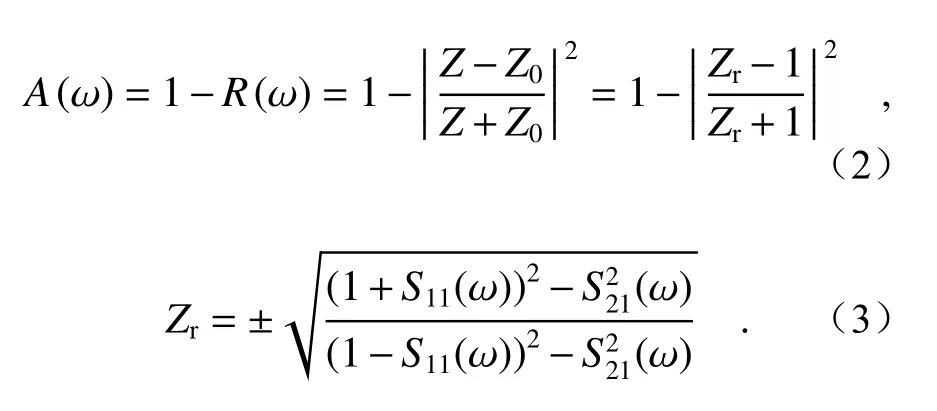
其中,Z0和Z分别是自由空间和吸收器的有效阻抗。而Zr=Z/Z0则是吸收器与自由空间之间的相对阻抗,当吸收器的阻抗与自由空间的阻抗相匹配时,即结构的相对阻抗Zr=1时,宽带吸收器的吸收率达到最大值。如图2(c)和2(d)显示了不同VO2电导率时相对阻抗的实部和虚部的变化情况。显然,随着电导率不断地增加,在1.34~2.25 THz范围内,实部逐渐接近于1的同时虚部逐渐接近于0,这意味着吸收器的有效阻抗和自由空间的有效阻抗之间逐渐匹配。当VO2处于金属态时,即σ(VO2)=2×10⁵S/m时,所设计结构同时获得了最高的吸收率和最宽的吸收带宽。
3.1 金属态时超材料可作为宽带吸收器
当VO2处于金属态时,设计的可切换超表面可以用作宽带吸收器,其由顶部金属开口谐振环嵌入一块VO2圆盘、上层PI介质、VO2薄膜组成.当VO2处于金属态时,底部金属相VO2作为反射层,可以阻止透射的发生。结构参数如图1所示,采用有限元方法对吸收器模型进行模拟,将单元格边界条件应用于x和y边界条件,并在z方向开放边界,入射太赫兹沿着-z方向入射。图3(彩图见期刊电子版)给出了VO2电导率为2×10⁵S/m(金属态)时宽带吸收器的反射、吸收光谱以及相对阻抗的实部、虚部。其中A(ω)表示吸收光谱,R(ω)表示反射光谱,Re(Zr)和Im(Zr)分别代表了宽带吸收器相对阻抗的实部和虚部。在1.53 THz和2.12 THz可以观察到2个不同的吸收峰,在1.34~2.25 THz频率范围内,所设计的结构可吸收90%以上的能量,带宽比(fmax-fmin)/[(fmax-fmin)/2][37]为50%,在1.10~3.18 THz频率范围内的吸收率大于50%,相应的带宽比为97%。其中如图1(a)所示,顶层VO2圆盘的引入改变了结构的有效阻抗,入射的电磁波与自由空间更加匹配,这也增强了结构整体的吸收性能。因此在1.53~2.12 THz的宽频范围内,所设计的宽带吸收器与自由空间实现了阻抗匹配,获得了较优的吸收和较宽的带宽。
一般来说,结构的几何参数对其共振频率和吸收率有一定的影响。同时,在器件加工过程中,也会在结构尺寸参数上引入误差。因此,本文对器件的结构参数进行了研究。在其他参数作为初始设置保持不变的情况下,研究了器件的太赫兹吸收谱随几何参数(α、Z3、R2)的变化规律,研究结果如图4(彩图见期刊电子版)所示。由图4(a)可以看出,吸收带宽随着开口角度α的增加而增大,中心频率1.84 THz随着α的增大呈轻微蓝移趋势,频率为1.53 THz处的谐振峰基本保持不变,频率为2.12 THz处的谐振峰呈蓝移趋势,由此得知,随开口角度α的增加,吸收带宽增大,吸收率降低。在图4(b)中,吸收峰强度首先随着Z3的增加而略微减少,在18 μm达到最佳吸收率,而后吸收率随着Z3的增加而减小。在图4(c)中,随着VO2圆盘半径R2的增加吸收带宽变化较小,吸收率略有下降,在47 μm处获得最佳的吸收率,并且当半径从44 μm增加到47 μm时,吸收曲线呈蓝移趋势。综上所述,与介质层厚度和VO2圆盘半径的影响相比,开口角度的变化对吸收带宽的影响效果更为显著。
为了进一步详细了解宽带吸收器的工作机理,研究了该宽带吸收器两个共振频率1.53 THz和2.12 THz处的电场分布,如图5所示。图5给出了入射太赫兹波为TE极化时吸收器在1.53 THz和2.12 THz处的电场分布。从图中可以看出,两个频率点处的电场主要分布在金属开口谐振环的开口两端、VO2圆盘靠近金属圆环开口处且沿着y轴方向;且相较于1.53 THz频率处的感应电场强度,2.21 THz频率处的电场强度更为聚集;此外,电场强度沿着VO2圆盘在与x轴平行且靠近金属圆环开口的内边缘逐渐减弱,这可能是由于VO2圆盘在与x轴平行靠近金属圆环开口的弱偶极子共振引起的。由于结构设计的对称性,入射波为TM极化时宽带吸收器在上述两个频率点处的电场分布整体展现出90°的旋转。
针对吸收器在实际应用中的需求,极化角度不敏感和入射角度不敏感性是非常重要的两大特性。图6(a)(彩图见期刊电子版)给出了在横电(TE)模式下,超材料吸收器吸收性能随入射太赫兹波频率以及入射角度的变化规律。根据计算结果,所设计的吸收器在0°~60°大入射角范围内仍展现出稳定的吸收率和较宽的工作带宽,具有较高的入射角容忍能力。当入射角大于60°时,其主吸收峰随着入射角的增大而变窄。因此,该吸收器即使在较大的入射角下,仍然能够提供较好的吸收特性。此外,对于TM极化,如图6(b)(彩图见期刊电子版)所示,吸收性能保持在8°以内的稳定。当入射角大于8°时,吸收带宽变窄,出现了一些高阶模态。在先前报道的基于VO2的吸收器[36]中也观察到吸收光谱对入射角的类似依赖性。因此,TE极化的吸收性能优于TM极化。同时还研究了入射太赫兹波的极化特性对吸收性能的影响。图6(c)(彩图见期刊电子版)给出了当太赫兹波垂直入射到吸收器表面时,极化角从0°变化到90°时的吸收率和频率的关系。从图6(b)可以看出,该宽带吸收器的吸收曲线是高度重合的,即在正常入射条件下,吸收器的吸收率与极化是完全无关的,这与吸收器单元结构在x和y方向上的对称性有着很大关系,大入射角度和极化不敏感特性在能量采集和光学传感中展现出较高的应用潜力。
3.2 绝缘态时超材料可作为窄带吸收器
当VO2为绝缘态时,该结构由顶部金属开口谐振环嵌入一块VO2圆盘、上层PI介质、VO2薄膜、下层PI介质、金属衬底组合构成多频带吸收器。采用电磁场数值模拟方法进行模拟研究,可得多频带吸收器的三峰吸收谱,图7展示了VO2电导率为200 S/m时窄带吸收器的反射、吸收光谱图以及相对阻抗的实部、虚部。可见,在2.4 THz~4 THz频率范围内存在3个吸收峰,其共振频率分别为2.54 THz、2.93 THz和3.34 THz,对应的吸收率分别为96%、99.9%和99.3%,对应半高宽(FWHM)[37]分别为93.6 GHz、206.7 GHz和39 GHz, 整体实现了多频带的完美吸收。从图6中还可看出,在多频吸收峰附近,阻抗实部逐渐接近于1,虚部逐渐接近0。在2.54 THz、2.93 THz、3.34 THz共振频率附近所设计的多频窄带吸收器都实现了窄带吸收器与自由空间之间的阻抗匹配。
固定其他参数的初始设置不变,研究几何参数(α、z1、W)对吸收率产生的影响,计算结果如图8(彩图见期刊电子版)所示。图8(a)中,随着开口角度(α)的增大吸收强度明显增加,对共振频率2.54 THz处的吸收率影响较为显著;在共振频率2.93 THz处,吸收率随着开口角度的增大而逐渐减小, 而在3.34 THz共振频率处吸收强度保持不变。在图8(b)中,下层PI介质厚度(z1)从44 μm以1 μm为步长变化增加至48 μm,对于2.93 THz和3.34 THz处的吸收峰变化影响较大,吸收率有所降低。z1在45 μm处达到最佳吸收曲线,之后随z1的增加整体吸收强度略有减小。在图8(c)中,随着金属开口环宽度(W)的增加,中间频带的吸收峰所受到的影响较大,在2 μm处获得最佳的吸收曲线,之后随着W的增加整体吸收强度反而减小。综上可看出,与介质层厚度和金属开口环宽度的影响相比,开口角度的影响效果更为显著。
此外,本文还研究了2.54 THz、2.93 THz和3.34 THz 3个吸收峰频率处的电场强度分布,如图(9)所示,给出了TE极化太赫兹波入射时3个吸收峰频率处的电场分布。在2.54 THz处,电场分布沿着金属开口谐振环的开口两端高度集中;在2.93 THz处,有部分能量均匀分布在吸收单元中心区域;在3.34 THz处,金属开口谐振环的开口两侧、吸收器单元结构中心区域范围内的电场强度很强。由于结构设计的对称性,入射波为TM极化时,窄带吸收器在上述3个频率点处的电场分布的结果整体展现了90°的旋转。
接下来,还研究了该多频带超材料吸收器在不同极化角度下的吸收特性。图10描述了极化角从0°以5°的步长增加到90°时吸收率与频率的变化规律。结果表明,TE模式下,当太赫兹波垂直入射到吸收器表面,本文中所提出的多频带超材料吸收器的吸收性能不随入射太赫兹波极化角度的变化而改变,其吸收曲线是高度重合的。极化角度的不敏感性与吸收器单元结构在x和y方向上的对称性有关。所设计结构的对称性这一内在原因确保了在正常入射下的极化不敏感性,这在许多应用中非常有帮助。
本文结构可以采用分子束外延法进行加工。2016年,Bian等人[38]利用分子束外延技术在单晶蓝宝石基底上生长可以精确控制厚度的VO2薄膜。2017年,孙洪君等人[39]采用分子束外延技术在单晶蓝宝石衬底上生长了高质量化学计量比VO2薄膜,通过该技术实现了薄膜厚度的精确控制。就本结构而言,可采用分子束外延在PI衬底上沉积薄VO2薄膜,再将圆盘结构引入到VO2薄膜的顶部。然后,在传统的光刻和金属化工艺的基础上,在PI上制备金微结构,形成金属CSRRS。本研究提出的设计方法为以连续VO2薄膜为基础,将完全不同的功能集成到一个结构中的多功能元器件的研究提供了新的途径。
本文所设计的太赫兹宽带吸收器主要可以应用于隐身和功能测量等方面。通过吸收太赫兹波,降低返回探测器的能量从而实现隐身,可以应用在雷达探测、现代战争武器等场合。同时,宽带吸收器可以应用于太赫兹波能量收集、测试计量领域,吸收器可以将吸收的能量转换为电能量从而实现能量测量。
4 结 论
本文设计了一种具有宽、窄频带特性的可切换双功能超材料吸收器,该吸收器由金属开口谐振环和VO2圆盘构成的顶层图案、上层PI介质层、VO2薄膜、下层PI介质层和底部金属衬底构成,通过外部电磁场、光场以及温度场等激励,可以使VO2发生绝缘态-金属态可逆相变过程,从而可以实现不同功能之间的转换。采用有限元方法对该可切换结构在0~4 THz频段进行数值模拟,结果表明:当VO2处于金属态时,此结构可以实现高性能太赫兹宽带吸收器功能,在1.55 THz~2.21 THz的频率范围内可实现98%的宽带吸收。当VO2从金属态转换为绝缘态时,此结构可以实现多频带窄带吸收器功能,所设计的超材料吸收器的共振频率为2.54 THz、2.93 THz、3.34 THz时,窄带吸收率在95%以上。此外,还讨论了几何参数对吸收率性能的影响。该吸收器件由于对称结构产生了极化不敏感性能,在大入射角时也表现出良好的吸收性能。本文提出的超材料吸收器具有结构简单、可切换功能和完美吸收等特性,可应用于太赫兹光电开关、电磁隐身、调制、热发射器和电磁能量采集等场合。

