A flexible ultra-broadband metamaterial absorber working on whole K-bands with polarization-insensitive and wide-angle stability
Tao Wang(汪涛) He-He He(何贺贺) Meng-Di Ding(丁梦迪)Jian-Bo Mao(毛剑波) Ren Sun(孙韧) and Lei Sheng(盛磊)
1School of Microelectronics,Hefei University of Technology,Hefei 230601,China
2School of Information Science and Technology,University of Science and Technology of China,Hefei 230027,China
3School of Electronic Science and Engineering,Southeast University,Nanjing 210096,China
4Technical Institute of Physics and Chemistry,Chinese Academy of Sciences,Beijing 100190,China
Keywords: flexible metamaterial absorber,periodic conductive patterns,ultra-broad band,wide-angle
1. Introduction
In recent years, with practical and potential applications in microwave stealth, satellite communications, electromagnetic (EM) compatibility, radar detection, and sensors, metamaterial absorber(MMA)has attracted extensive attention in these fields.[1,2]Nowadays, mostly advanced satellite communications and radar detections for military applications are working in the frequency range of 12 GHz-40 GHz,i.e.,the whole K-bands, which maintains Ku, K, and Ka bands.In these applications, MMA should be conformal with the surface of object to absorb various incident EM waves, but commonly MMAs always select FR-4 as substrate to obtain high absorption,[3,4]these rigid and bulky absorbers can only conformal with flat surface, which impede the adoption of MMA on curved surfaces,such as plane,satellite,and missile.In order to achieve practical concrete requirements, flexible,lightweight, easy-processing MMAs that can be conformal with curved surfaces of objects using for K-bands microwave absorbing should be explored.
Nowadays, it is quite difficult to design and fabricate a flexible ultra-broadband MMA, due to the periodic conductive patterns is very difficult to transfer on the flexible substrate, such as PVC and PTFE,and the technological process is quite sophisticated which lead to a plenty of errors and deviations of the products. Moreover,deformation magnitude of periodic conductive patterns and substrate is quite disagreement when the absorber is bent in an arc,which results in poor performance when MMA is conformal with a curved surface.Recently, three-dimensional (3D) printing technology is usually used in MMA fabrication, but it is not suitable for the manufacture of flexible absorbers due to the bad mechanical flexibility of the 3D structure.[5,6]Fortunately, more additive manufacturing methods such as template printing and spraying can be used for the manufacture of flexible MMA.Especially,using screen-printing technology, single-layer or multi-layer absorbers can be fabricated on different flexible substrates,such as polyethylene terephthalate(PET),polydimethylsiloxane(PDMS),polyimide(PI),and so forth.[7,8]
Up to date, through accurate regulation of the printing process, conductive ink can achieve efficient absorption from microwave to terahertz, or even in light bands.[9-14]Kimet al. reported a narrow-band flexible absorber with absorptivity over 99%at 9.21 GHz using an improved Jerusalem-cross annular resonator.[9]Genget al. reported a multi-layer flexible MMA operating in terahertz band using gold split-ring resonators, proving its wide applications in biosensors.[15]Huanget al.using layer-by-layer screen overprinting method produced a flexible MMA with absorptivity greater than 90% at 8.3 GHz-10.9 GHz.[16]Wuet al. reported a broadband millimeter-wave absorber with mechanical flexibility and optical transparency in the frequency range of 73.5 GHz-110 GHz.[17]Lvet al. reported a flexible electric-driven device composed of an insulating organic polymer substrate, a carriers transport layer, and a core-shell absorber, which can achieve narrow-band adjustable and effective absorption below 2 GHz by controlling the external voltage.[18]The above literatures on flexible MMA mostly focused on the efficient absorption of high frequency or narrowband, a flexible ultrabroadband absorber working on the frequency range covering the whole K-bands from 12 GHz to 40 GHz is still not been reported.
To effectively absorb microwaves in the whole K-bands on a curved surface, a flexible sandwich MMA composed of PVC-PI-PTFE-metal plate is designed,analyzed,fabricated,and measured. All the conductive patterns are printed by silver conductive ink and located on a surface of flexible thin PI substrate. Traditionally,FSS is printed on the upper surface of the PI layer,it is worth noting that FSS in this proposed structure is arranged on the lower surface of the PI layer which directly results in the improvement of microwave absorption.Absorptivity of the proposed flexible absorber is more than 90%at 10.47 GHz-45.44 GHz, which contains the whole Kbands and portion of X-band and U-band. The consistency of simulation and measurement proves good flexibility and robustness of the flexible absorber.
2. Physical model of the flexible absorber
To explore the design method, working principle, and manufacture technology for flexible ultra-broadband absorber,as an example to illustrate the concept,a flexible absorber with PVC-PI-PTFE-metal plate structure is modeled herein. Incident wave from free space penetrate PVC, PI, and PTFE in turn, and is totally reflected by metal plate. Geometry of the unit cell is depicted in Fig. 1. Acted as a metallic ground plate, copper with thickness of 0.017 mm is attached on the lowest level of the unit cell and is combined with PTFE layer.Square conductive pattern is printed on the lower surface of PI (ε= 3.24+j0.031) layer, with resistance of 120 Ω/sq.Dielectric constants of PTFE and PVC are 2.1+j0.001 and 2.56+j0.025,respectively. Optimized parameters are as follows:a=4.2 mm,dPI=0.15 mm,dPTFE=1.7 mm,dPVC=1.5 mm.

Fig.1. Physical model of the flexible absorber.
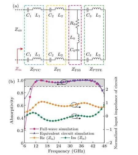
Fig.2. Calibration of the physical model. (a)Equivalent circuit of the physical model. (b)Physical model analysis versus full-wave analysis.
According to the working principle of MMA, absorption efficiency is determined by two major factors, one is the impedance matching between absorber and free space, the other is intensively EM loss caused by the materials of every layer. Based on equivalent circuit model,[19]FSS herein is developed as a band-stop resonating surface with a series ofR-L-Ccircuits in Fig.2(a),and absorption of this MMA is mainly caused by two adjacent resonances between FSS and grounded metal plate.ZFSSrepresents equivalent impedance of resistive film,andZinis input impedance of parallel circuit constituted byZFSSand transmission lines of each dielectric layer. Each equivalent parameter is calculated and optimized by simulation analysis. Normalized input impedance is analyzed as shown in Fig. 2(b), real part ofZinis near unity,and imaginary part is close to zero in 10.47 GHz-45.44 GHz.It is noticeable that equivalent circuit can achieve excellent impedance matching in the range of 10.47 GHz-45.44 GHz.
To verify accuracy of the equivalent circuit model for flexible MMA, the calculated results from the equivalent circuit are compared against that obtained by the full-wave simulation analysis. Absorptivity of the flexible MMA can be characterized asA= 1-|S11|2-|S21|2, whereS11andS21represent reflection and transmission coefficients of the unit cell,respectively. Transmission coefficient is zero because of obstruction of the copper ground plate, as we all know, EM waves cannot penetrate metal plate, so the absorptivity is determined asA= 1-|S11|2. According to absorption spectrum in Fig.2(b),absorptivity is higher than 90%in frequency range of 10.47 GHz-45.44 GHz under normal incidence,and absorptivity is more than 96% in 11.25 GHz-43.69 GHz. It should be pointed out that two significant absorption peaks are observed at 13.91 GHz and 37.63 GHz, and the corresponding absorptivity is 99.88%and 99.99%,respectively. The absorptivity deduced from equivalent circuit is compared with that from full-wave analysis, and the two curves show good agreement except for small deviations as depicted in Fig.2(b),which means that the equivalent circuit model is quite effective and can be used for the design of a flexible MMA,and the ultra-broadband absorption is caused by two perfectR-L-Cresonances in the stacked layers.
3. Results and discussion
According to equivalent medium theory, some major properties of the flexible absorber are obtained fromSparameters based on Nicolson-Ross-Weir (NRW) method.[20]Permittivity,permeability,and equivalent impedance of the flexible MMA with thickness ofdcan be calculated by
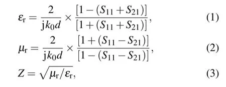
where wavenumberk0=2π f/c,fis microwave frequency,andcis speed of light. Results of the unit cell are presented in Fig. 3. It can be seen from Fig. 3(a) that real part of permittivity and permeability is negative alternately, which verifies single negative behavior of the flexible MMA.Figure 3(b)illustrates normalized impedance of the flexible MMA, it can be observed that there is a good input impedance matching between flexible MMA and free space, so that the backward reflection at the interface of MMA and free space is effectively reduced, which means that almost all of the incident wave is absorbed by the MMA.Impedance matching can be attributed to the appropriate input impedance of MMA designed by equivalent circuit model, which further verifies the effectively of modified circuit model and equivalent medium theory used in this work.

Fig. 3. Crucial physical characters of the flexible absorber. (a) Complex permittivity and permeability. (b)Effective impedance.
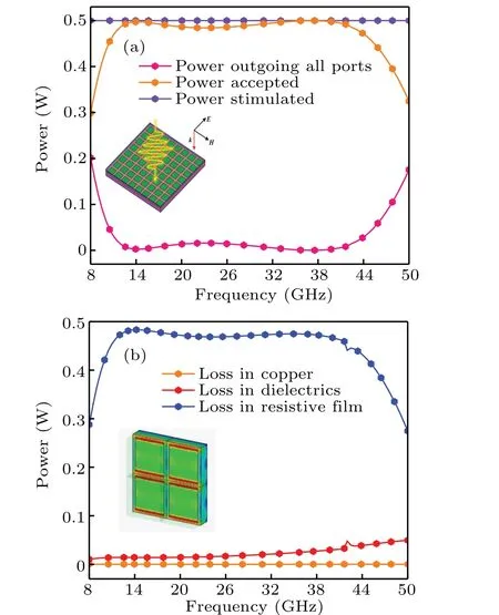
Fig. 4. Energy analysis of the flexible absorber: (a) energy directions and(b)power loss distributions.
To gain insight into resonances absorption of the flexible MMA,power loss of each layer is analyzed.The percentage of power loss at each layer is presented in Fig.4. Combined with impedance conditions in Fig.3(b),figure 4(a)shows that more than 98% energy of the incident EM waves entered into the absorber in frequency range of 10.47 GHz-45.44 GHz,which means that only less than 2% of the incident waves are reflected from MMA to air. Figure 4(b) further illustrates perspective view of power loss of entered energy in the absorber,it can be seen that mostly power loss is focused on resistance film layer except less than 5% occurred in dielectrics layers,which means that resistance film layer is mainly responsible for the absorbing performance of this flexible MMA.
To explore wave absorption mechanism of the proposed MMA,distribution of surface current and electric field at frequencies of 13.91 GHz and 37.63 GHz are simulated using near field conditions. Figures 5(a)and 5(b)show the comparison of surface current between FSS layer and ground plate layer,an equivalent surface current at 13.91 GHz on FSS layer is mainly concentrated at the center area,which is antiparallel to the current flowing through the metallic ground plate. As a result,magnetic resonance occurred when a plane EM wave incident to the surface of MMA, so an equivalent circulating current is formed between the resistive film layer and ground plate layer.[21]For the similar reason, surface current formed by FSS layer at 37.63 GHz is antiparallel to the current on ground layer,while some parallel current at the center area is caused by electrical resonance. As compared in Figs. 5(c)-5(d),antiparallel currents are much stronger than parallel currents, so magnetic resonance is the key factor of EM wave absorption at 37.63 GHz. Figures 5(e)-5(f)show electric field distribution of FSS layer at two resonance frequencies,i.e.,13.91 GHz and 37.63 GHz, it can be observed that the electric fields are mainly concentrated on the fringe of FSS layer,so the resonance is closely related to the side length of FSS layer.[22]
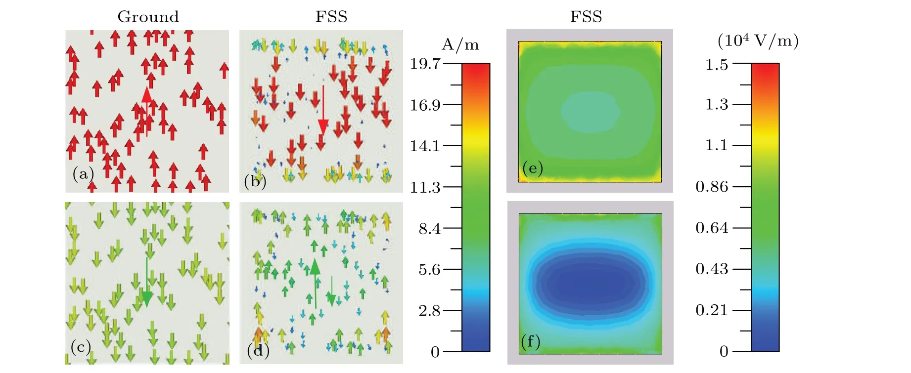
Fig.5. Surface current[(a)-(d)]and electric field[(e)-(f)]analysis on crucial layer of flexible absorber;(a)metallic ground at 13.91 GHz;(b)FSS at 13.91 GHz;(c)metallic ground at 37.63 GHz;(d)FSS at 37.63 GHz;(e)FSS at 13.91 GHz;and(f)FSS at 37.63 GHz.

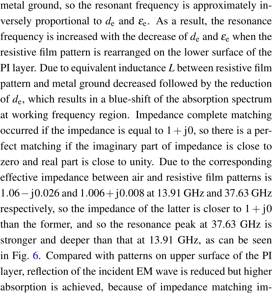

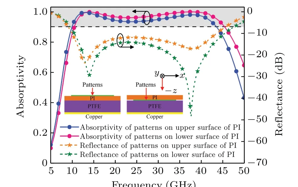
Fig. 6. Reflectance and absorbing performance of the flexible MMA with patterns on upper versus lower surface of the PI layer.
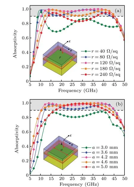
Fig. 7. Influence of resistance and size of FSS patterns on absorption frequency spectrum: (a)various resistances of FSS and(b)various sizes of the unit cell.
To further investigate sensitivity of absorption on resistive film patterns,numerical simulations are provided by changing resistancerand unit sizeaof resistive film as shown in Fig.7.It should be noted that the absorption spectrum occurs a blueshift with increasingr,while the absorptivity increased firstly and decreased later,as mentioned above,this is caused by variation of impedance matching between air and resistive film patterns. Furthermore, the absorption band expands to both sides firstly and shrinks later,whenaincreased from 3 mm to 5 mm. So the best absorption response can be obtained when resistance value and unit size is properly compromised and optimized.
To reduce RCS of targets equipped with an MMA for stealth, EM control ability of the flexible MMA is explored.As shown in Fig.8,the simulated RCS reduction of the MMA reveals that there are two reduction peaks at 16.1 GHz and 36.81 GHz, with RCS reduction of 30.13 dB and 28.96 dB,respectively. Moreover, RCS reduction is much more than 10 dB in frequency band of 11.48 GHz-43.87 GHz,with relative bandwidth of 117%.
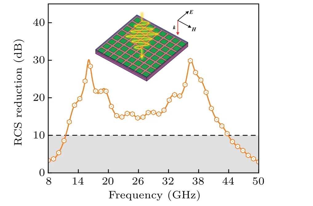
Fig. 8. RCS reduction performance of incident microwaves with different frequencies.

Fig. 9. The absorption spectrum with different incident angles of the EM waves: (a)TE wave and(b)TM wave.
As aforementioned, absorption efficiency of MMA may be influenced by oblique incident and polarization angles of EM waves, and so the sensitivity of the absorber should be investigated. Due to the symmetry of the unit cell,the absorption is insensitive to incident polarization. To explore whether the flexible MMA can maintain ultra-broadband and highabsorption characteristics under conformal conditions,the absorption spectra under different oblique incidences are studied.The absorption spectrum is depicted in Fig. 9, when oblique incident angle is less than 55°, the flexible MMA still maintains more than 90% absorptivity for both transverse electric(TE)polarized wave and transverse magnetic(TM)polarized wave. Results of this MMA provide an essential reference for surface conformal of objects which should be insensitive to polarization and incidence.
4. Fabrication and measurement verification
To verify performance of the proposed flexible MMA,the structural prototype is fabricated as shown in Fig. 10. Because all patterns are located on the surface of the PI layer,the processing technology is quite simple. To increase precision of experimental testing, according to periodicity and symmetry of the MMA, overall size of the sample processed by screen-printing technology is 150 mm×150 mm with the whole weight of 132 g. Conductive ink in this technology is consist of carbon black, silver particles, water, and a certain proportion of emulsion,and resistance of ink film layer is adjusted by thickness of ink film. After heating and curing, all FSS patterns with specific resistances are produced by square areas filled with ink,and the printed block resistors are in close contact with the polymer substrate,which helps to reduce parasitic effects. A surface image of the resistive film under an electron microscope is shown in Fig.10(b). Resistance of the FSS film is measured using a four-probe resistance tester(ST-2258C), and a calibrated Rohde & Schwarz ZVA 40 vector network analyzer and two horn antennas are used to measure the fabricated prototype in microwave anechoic chamber.
As shown in Fig. 11, the measurement of the proposed absorber under normal incidence exhibits a close similarity with the simulation except a slight red-shift, which demonstrates the accuracy of the simulation and the physical model of the MMA, and the little deviation is mainly caused by the machining precision and parasitic effects. To explore the effect of resistive film rearrangement of the PI layer,absorption spectrum of resistive film on upper surface of PI is measured and compared with that on lower surface of PI,as is depicted in Fig.12(a). It can be seen from the normalized absorptivity that the resistive film patterns exhibits better absorption characteristics when it is located on the lower surface of PI.

Fig. 10. Photographs of the fabricated flexible MMA for test: (a) curved flexible MMA; (b) a unit cell in electron microscope test (Eclipse E200);(c)weight of the prototype;(d)size of the prototype;and(e)measurement system in microwave anechoic chamber.
To measure the flexibility of the proposed absorber, the prototype is attached on the outside surface of a cylinder with diameters of 100 mm and 200 mm, respectively. As normalized absorption spectrum is presented in Fig.12(b),strong absorption can be observed in a frequency range of 10 GHz-40 GHz under different bending degrees. When the curvature of the cylinder increased,the size of the effective caliber area decreased, which deteriorated absorbing performance of the flexible MMA. Fortunately, high-efficiency absorption over 80%can still be obtained when diameter of the cylinder is not less than 100 mm,which means that the flexible MMA can be conformal on an object with different curvature surfaces.
A comprehensive comparison of the purposed flexible MMA with other similar microwave absorbers is presented in Table 1, whereλmaxis the largest wavelength in absorption spectrum. Some crucial parameters such as absorption bandwidth, relative bandwidth, periodicity, and thickness of MMA are listed herein. Compared with other MMAs,[24-27]the purposed MMA is flexible and covers the whole Ku, K,Ka bands, and some of X, U bands. Furthermore, due to the pattern is located on the lower surface of the PI layer,the resonance peaks at 13.91 GHz and 37.63 GHz is improved obviously.It should be pointed out that the absorber reported in the present research is structurally different from other absorbers and shows the ultra-broadband microwave absorption and the excellent flexibility.

Fig.11. Measured reflectance and normalized absorptivity of the fabricated flexible prototype MMA.

Fig.12. Comparison of measured absorption spectra under different conditions: (a) patterns on upper versus lower surface of the PI layer; (b) without curve versus on a cylinder with D=200 mm versus on a cylinder with D=100 mm.

Table 1. Comprehensive comparison of the proposed flexible MMA with typically reported absorbers.
5. Conclusion
A flexible MMA working on all K-bands with ultrabroadband, polarization-insensitive, and wide-angle stability is designed by equivalent circuit model, simulated by fullwave analysis method, fabricated by screen-printing technology, measured by a vector network analyzer, and compared with some typical MMAs. Different from the reported absorbers, resistive film patterns are arranged on the lower surface of the PI layer in this work, which leads to the improvement of microwave absorbing performance. Based on equivalent circuit model and equivalent medium theory, the absorption mechanism is analyzed and verified by numerical simulations. The simulated results show that the flexible MMA can obtain absorptivity greater than 90% in the whole Ku, K, Ka bands, and parts of X and U bands, and the absorptivity can even exceed 96% in the frequency range of 11.25 GHz-43.69 GHz. Absorption spectra under different polarizations and oblique incidences indicate that the absorber is polarization-insensitive and wide-angled. The free-space method is used to measure the fabricated prototype, and experimental results show good agreement with numerical results. Due to characteristics of easy conformal, high absorption,and ultra-broadband,the flexible MMA is applicable for EM shielding,radar stealth,sensors,and satellite communications working on the K-band.
Acknowledgements
Project supported by the Fundamental Research Funds for the Central Universities of China (Grant No. JD2020JGPY0010), the China Post-doctoral Science Foundation (Grant No. 2020M671834), and the Anhui Province Post-doctoral Science Foundation, China (Grant No.2020A397).
- Chinese Physics B的其它文章
- Surface modulation of halide perovskite films for efficient and stable solar cells
- Graphene-based heterojunction for enhanced photodetectors
- Lithium ion batteries cathode material: V2O5
- A review on 3d transition metal dilute magnetic REIn3 intermetallic compounds
- Charge transfer modification of inverted planar perovskite solar cells by NiOx/Sr:NiOx bilayer hole transport layer
- A low-cost invasive microwave ablation antenna with a directional heating pattern

