
Low-thermal-budget Au-free ohmic contact to an ultrathin barrier AlGaN/GaN heterostructure utilizing a micro-patterned ohmic recess
2021-09-18 02:01:04WenShiSenHuangXinhuaWangQimengJiangYixuYaoLanBiYuchenLiKexinDengJieFanHaiboYinKeWeiYankuiLiJingyuanShiHaojieJiangJunfengLiandXinyuLiu
Journal of Semiconductors 2021年9期
Wen Shi ,Sen Huang , ,Xinhua Wang ,,Qimeng Jiang,Yixu Yao,Lan Bi,Yuchen Li,Kexin Deng,Jie Fan,Haibo Yin,Ke Wei,Yankui Li,Jingyuan Shi,Haojie Jiang,Junfeng Li,and Xinyu Liu,
1Key Laboratory of Microelectronic Devices & Integrated Technology,Institute of Microelectronics,Chinese Academy of Sciences,Beijing 100029,China
2Institute of Microelectronics,University of Chinese Academy of Sciences,Beijing 100049,China
Abstract:A pre-ohmic micro-patterned recess process,is utilized to fabricate Ti/Al/Ti/TiN ohmic contact to an ultrathin-barrier(UTB) AlGaN/GaN heterostructure,featuring a significantly reduced ohmic contact resistivity of 0.56 Ω·mm at an alloy temperature of 550 °C.The sheet resistances increase with the temperature following a power law with the index of +2.58,while the specific contact resistivity decreases with the temperature.The contact mechanism can be well described by thermionic field emission (TFE).The extracted Schottky barrier height and electron concentration are 0.31 eV and 5.52 × 1018 cm−3,which suggests an intimate contact between ohmic metal and the UTB-AlGaN as well as GaN buffer.A good correlation between ohmic transfer length and the micro-pattern size is revealed,though in-depth investigation is needed.A preliminary CMOS-process-compatible metal–insulator–semiconductor high-mobility transistor (MIS-HEMT) was fabricated with the proposed Au-free ohmic contact technique.
Key words:ultrathin-barrier AlGaN/GaN heterostructure;low thermal budget;Au-free ohmic contact;micro-patterned ohmic recess;MIS-HEMTs;transfer length
1.Introduction
The good potential of the ultrathin barrier (UTB) AlGaN/GaN heterostructure has been demonstrated in the fabrication of high uniformity GaN-on-Si power devices and integration of peripheral controlling circuits[1−4].To integrate GaN power devices with GaN-or even Si-based ICs on the UTBAlGaN/GaN platform[5,6],it is highly desirable to develop a CMOS-compatible process[7],in which a low contact resistivity Au-free ohmic contact is critical to both GaN power and RF devices[8−16].
Regrowth of n-type GaN on source–drain region is an effective way to reduceRcto 0.05–0.15 Ω·mm[17,18].However,the procedure adds complexity and a high maintenance cost.N-doped in the ohmic region by ion implantation is also useful while extremely high annealing temperature is needed[19].Utilizing the TixAlyalloy instead of multilayers as contact metal schemes has been demonstrated as being efficient but the required annealing temperature is also high (880 °C)[14].A low annealing temperature of less than 650 °C is preferred for the Au-free ohmic contact,in order to mitigate high-temperature annealing-induced degradation of the III-nitride surface and dielectric/III-nitride interface[15,16].Previous study has optimized the over-etching condition of a low-pressure chemical vapor deposited SiNx(LPCVD-SiNx) passivation layer on the UTB-AlGaN/GaN heterostructure[16],while the obtained ohmic contact resistivityRCof 1.57 Ω·mm remains too high.
To break theRClimit of the uniform-ohmic-recess process,a patterned AlGaN layer structure was proposed on Ti/Al/Ni/Au ohmic contact to a conventional AlGaN/GaN heterostructure[17,18].However,further research is needed to investigate the effect of such patterning processes on the Aufree ohmic contact to ultrathin-barrier heterostructures.In this work,to lower down the Ti/Al/Ti/TiN-based Au-free ohmic contact to the UTB-AlGaN/GaN heterostructure,a grid-patterned ohmic-recess process with good over-etching tolerance was developed.A significantly reducedRCof 0.56 Ω·mm was realized at a relative low annealing temperature of 550 °C.CMOS-compatible GaN MIS-HEMTs was also fabricated on the UTB-AlGaN/GaN on the Si platform.
2.Device fabrication
The schematic cross section of the fabricated CMOScompatible LPCVD-SiNx/AlGaN/GaN MIS-HEMTs is depicted in Fig.1(a).The UTB-AlGaN/GaN heterostructure wafer used in this work was grown by metal organic chemical vapor deposition (MOCVD) on a 3-inch Si substrate.
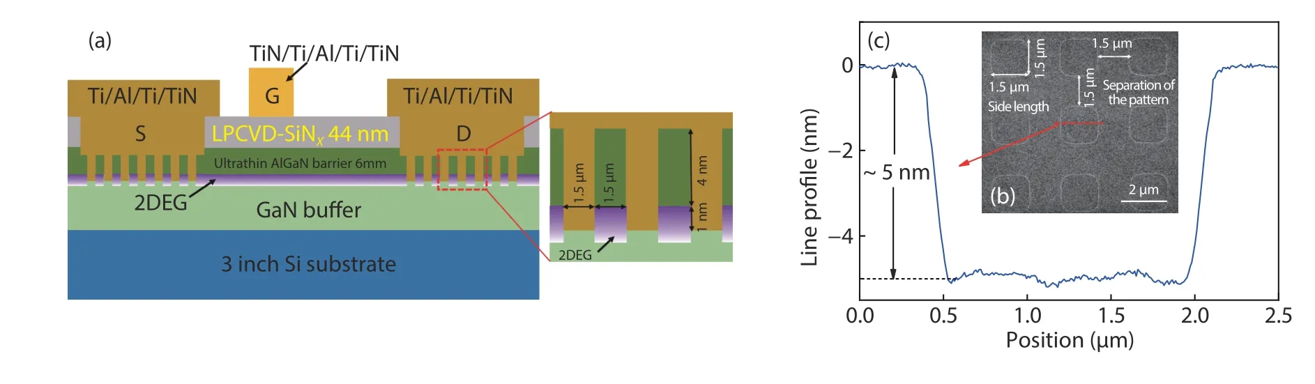
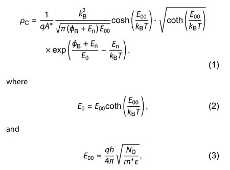
Fig.1.(Color online) (a) Schematic cross section of the fabricated Si-CMOS-compatible GaN MIS-HEMTs utilizing a micro-patterned ohmic recess.(b) SEM image.(c) Line profile of the micro-patterned AlGaN/GaN heterostructure measured by atomic force microscopy (AFM).
The AlGaN barrier consists of a~1 nm GaN cap,a~4 nm Al0.25Ga0.75N layer and a~1 nm AlN interface enhancement layer.The fresh wafers were first cleaned by standard Radio Corporation of America (RCA) treatment,followed by a~44 nm LPCVD-SiNxdeposited immediately at 780 °C.The high deposition temperature ensures compact film quality and good thermal stability of the SiNxfilm,and moreover provides sufficient thermal budget for the subsequent process[4].The LPCVD-SiNxlayer in the ohmic region was then etched away by low power SF6/CHF3hybrid plasmas with 20% over-etching time[16],yielding a squared ohmic contact region of 100 ×100μm2.The 20% over etching resulted in about 2 nm Al-GaN barrier removal.Another photolithography was conducted to form uniformly distributed square patterns with separation equal to the side length in the ohmic contact area,as shown in Fig.1(a).Chlorine-based plasmas were adopted to etching through the AlGaN barrier to expose the GaN buffer.The sides and adjacent spacing of square holes are both 1.5μm,as measured by a scanning electron microscope(SEM) shown in Fig.1(b).The recess depth is determined to be~5 nm (corresponding to~1 nm over recess of GaN buffer) by an atomic force microscope (AFM),as shown in Fig.1(c).Then,device isolation was realized by multi-energy argon ion implantation.
The Ti/Al/Ti/TiN ohmic metal stack was then sputtered to cover the ohmic contact region by another photolithography with a proper wet treatment of the etched surface.The source-drain ohmic contact was then annealed at 550 °C for 90 s in N2ambient.Subsequently,a TiN/Ti/Al/Ti/TiN metal stack was sputtered over the LPCVD-SiNxlayer to form a MISgated structure.The fabricated MIS-HEMTs were finally annealed at 280 °C for 4 min in N2ambient to further improve the thermal stability of the gate.The gate lengthLG,gate-tosourceLGS,and gate-to-drain distanceLGSof the MIS-HEMTs are 2.25,1.25,and 1.75μm,respectively.
3.Results and discussion
The transmission line method (TLM) was used for the determination ofRCandRSHfor the Au-free ohmic contact utilizing a pre-ohmic micro-patterned recess process,as shown in Fig.2(a).The typicalRCof the Au-free ohmic contact is determined to be 0.56 Ω·mm,about one-third of our previous reported value (1.57 Ω·mm) without the micro-patterned ohmic recess[16].The corresponding sheet resistanceRSHis extracted to be 385 Ω/sq,indicating that the charge-modulated LPCVDSiNxlayer has recovered the 2DEG effectively.To verify the process window of such a micro-patterned ohmic recess,another ohmic-patterned sample with about a 10-nm over-recess of the GaN channel was also fabricated,only resulting in a slight increase ofRC,from 0.56 to 0.58 Ω·mm,while with comparableRSH(399 versus 385 Ω/sq),as shown in Fig.2(a).
Temperature-dependent four-probe measurement was conducted from–50 to 200 °C,in an N2protecting environment,to explore the contact mechanism of the fabricated Au-free ohmic contact (Fig.2(b)).RCis observed to vary slightly over the temperature range,whileRSHincreases with the temperature.The latter is due to optical phonon scattering induced by degradation of 2-D electron gas (2DEG) mobility at high temperature (T>~ 200 K)[19−21].In this case,the mobility follows a power law against temperature,sinceRSH,which is inversely proportional to the mobility,has a powerlaw relation with a negative power factor[20−22].Fig.2(b)shows the fitting curve ofRSHand the extracted power index of +2.58 is consistent with reported values[21].The corresponding specific contact resistivityρCshown in Fig.2(c) decreases from 1.95 × 10⁻⁵to 2.01 × 10⁻⁶Ω·cm2when the temperature increases from–50 to 200 °C[16].Both ohmic contact mechanisms of the patterned and un-patterned ohmic contacts can be well fitted by the thermionic field emission (TFE) mechanism shown below[16,20,23],
whereA*=4πm*kB2/h3is the effective Richardson constant,m*is the effective mass of the tunneling electrons in (Al)GaN,εis the dielectric constant of (Al)GaN,ФBis Schottky barrier height between (Al)GaN and the ohmic metals,NDis electron carrier concentration,andEnis the energy difference between the conduction-band edge and the Fermi level at the AlGaN/GaN interface.
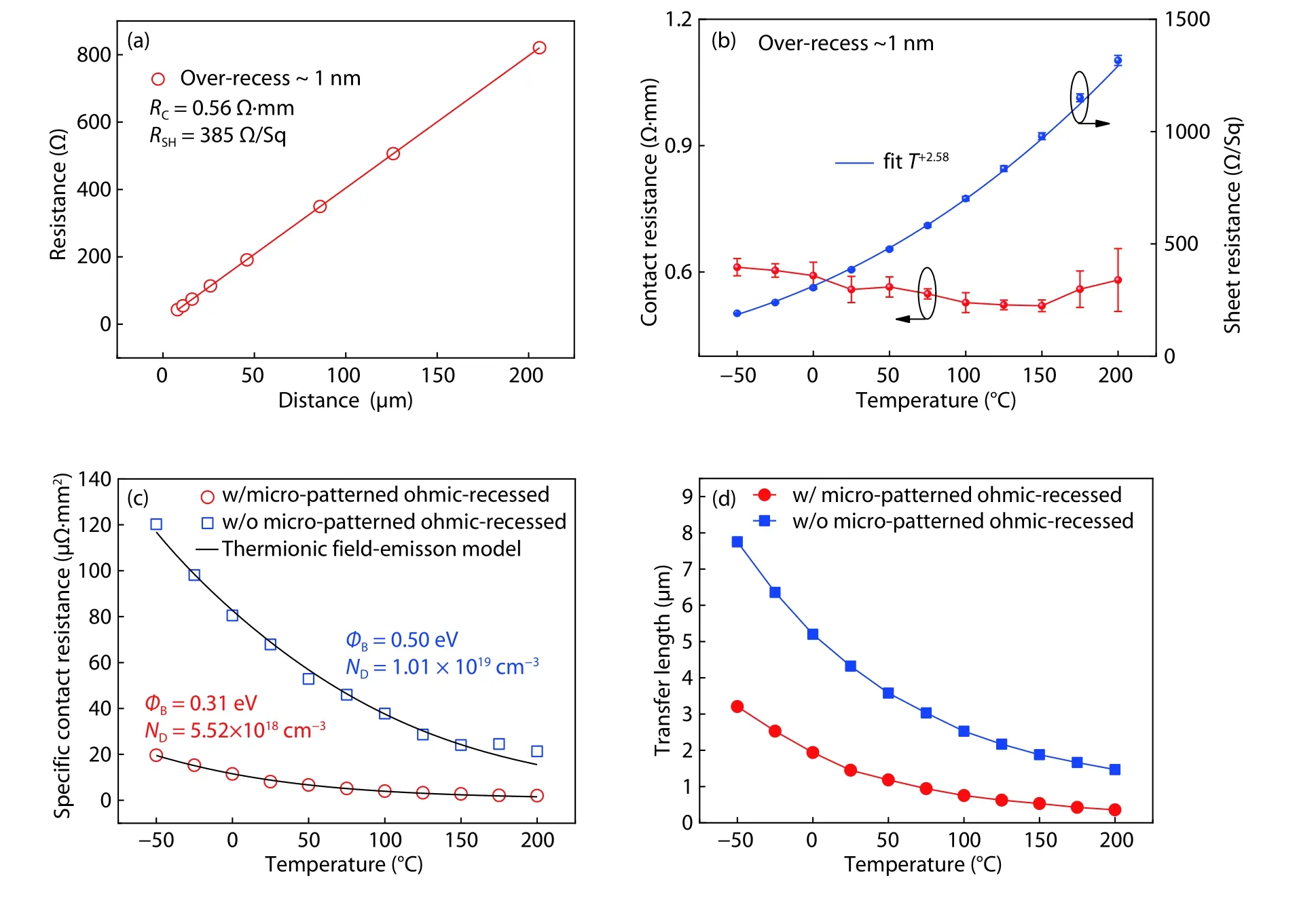
Fig.2.(a) Linear fit of the fabricated Ti/Al/Ti/TiN ohmic contact resistances versus TLM spacing.(b) Temperature-dependent characteristics:RC and RSH.(c) ρC as fitted by thermionic field emission model.(d) Temperature-dependent transfer length LT.
As for the patterned ohmic contact,the TFE fitting yields a Schottky barrier heightФBof 0.31 eV and aNDof 5.5 ×1018cm–3,in contrast to the value of 0.50 eV and 1.01 ×1019cm–3obtained in the un-patterned sample.The lowerФBis due to partial transition of metal/AlGaN to metal/GaN contact because of over-etching of the AlGaN barrier.However,over-etching also results in 2DEG depletion in the micro-patterned region,giving rise to a reducedND.Further investigation is ongoing to verify the trade-off betweenФBandNDand their effects onρc.Transfer lengthLTof the fabricated ohmic contacts have also been plotted in Fig.2(d) with the temperature.The micro-pattern ohmic recess leads to a remarkable reduction ofLTin the measured range.And the shorter current flow distance from the metal (semiconductor) to the semiconductor (metal) can be attributed to the larger lateral contact area to collect current.
To shed light on the effect of pattern size on the contact resistance,a survey of state-of-the-art ohmic contacts that adopts a similar pre-ohmic pattern process is summarized in Table 1.It can be observed that whether the AlGaN barrier in the patterned region is partially or fully recessed,the change ofLTfollows closely with the pattern separation.For instance,LTdecreases from 1.45 to 0.35μm as the separation is reduced from 1.50 (this work) to 0.50μm[17].However,there is little correlation between transfer length value and the overrecess depth,since theLTof ohmic-patterned sample with a~1 nm and~10 nm over-recess are the same.Further study is needed to investigate the mechanism behind the correlation betweenLTand the separation of the micro-pattern.Anyway,the micro-patterned ohmic recess could be an efficient method to reduceRCandLTin Au-free ohmic contacts to the UTBAlGaN/GaN heterostructure,and the shrinking ofLTwill also do good to the scaling down of the active chip area of GaNbased electronic devices.
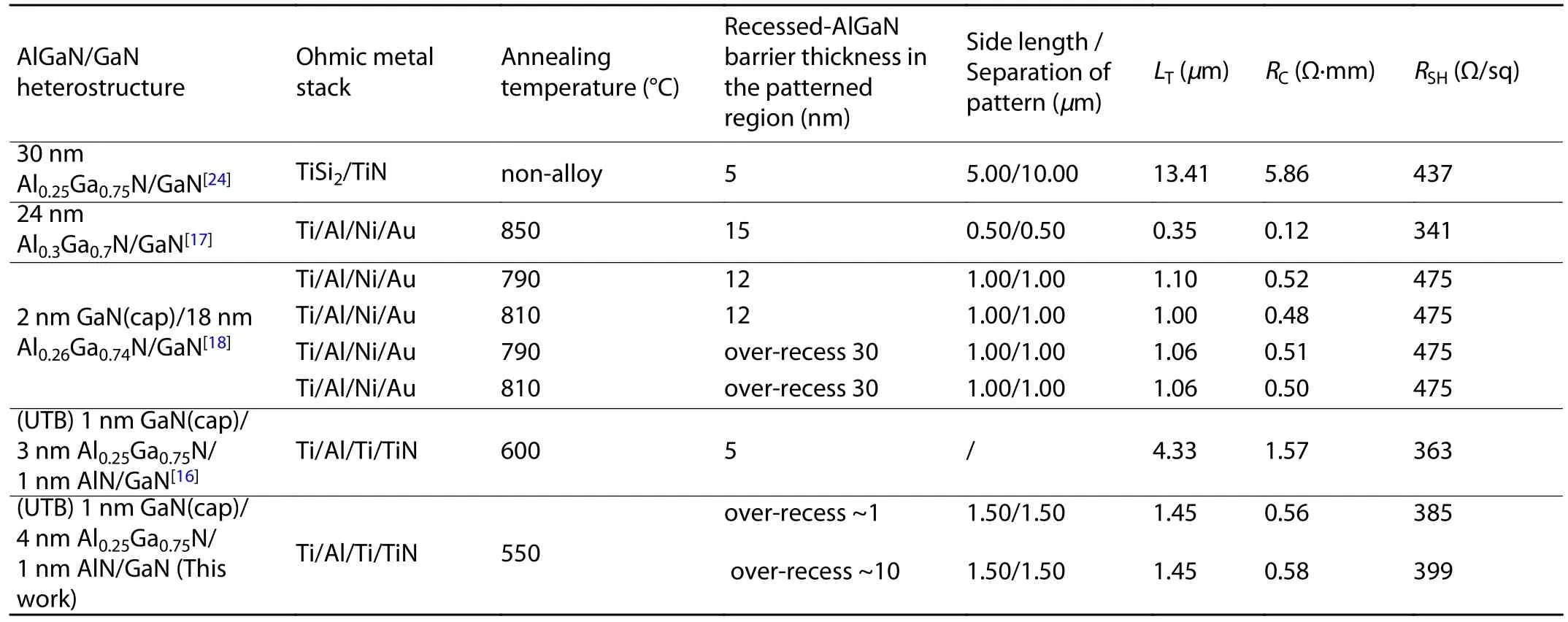
Table 1.The summary of micro-patterned ohmic contacts to various AlGaN/GaN heterostructures.
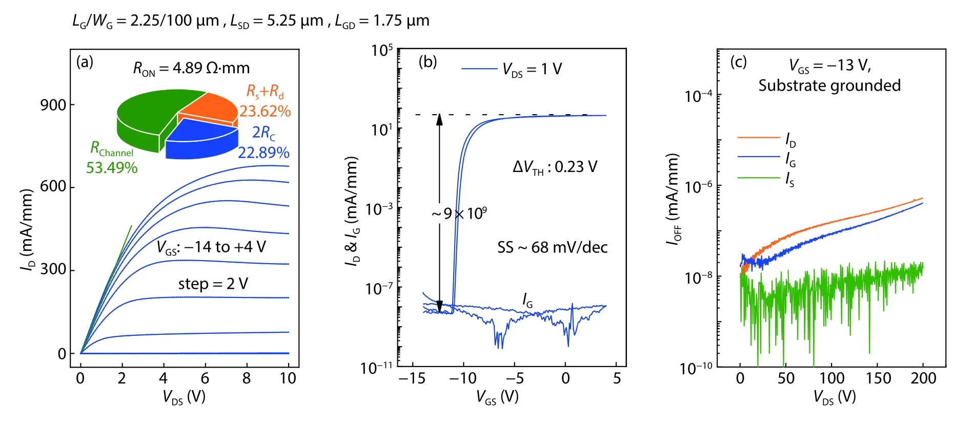
Fig.3.(Color online) (a) DC output,(b) transfer,and (c) off-state leakage characteristics of the fabricated CMOS-process compatible LPCVD-SiNx/AlGaN/GaN MIS-HEMTs.
The pre-ohmic micro-pattered recess process was then implemented in a fabrication of CMOS-compatible LPCVDSiNx/AlGaN/GaN MIS-HEMTs,with LPCVD-SiNxserving as the gate dielectric.The MIS-HEMTs’ output characteristics are shown in Fig.3(a).The on-state resistance (RON),as extracted from the linear region of the output curve,composed of ohmic contact resistance 2RC(22.89%),access region resistanceRs+Rd(23.62%) and gate channel resistanceRChannel(53.49%),is substantially low owing to the ohmic pattern process.High ON/OFF current ratios (ION/IOFF) are more than 9 ×10¹⁰while low gate leakage (~10–7mA/mm) is also obtained in transfer measurements (Fig.3(b)),thanks to the high insulating behavior of the LPCVD-SiNxgate dielectric.Due to the trapping behavior of deep states located at the LPCVDSiNx/GaN interface,a clockwise threshold voltage (VTH) hysteresis of 0.23 V is observed at a drain bias of 1 V (Fig.3(b)).A smallerVTHhysteresis,while a relative lower extrinsic transconductance,can be further realized with proper surface treatments[1].Moreover,the OFF-state drain and gate current of the MIS-HEMTs withLGDof 1.75μm,are well suppressed towardsVDSof 200 V (Fig.3(c)).Further work on the implementation of the micro-patterned ohmic recess in enhancementmode AlGaN/GaN (MIS)HEMTs is ongoing.
4.Conclusion
A pre-ohmic micro-patterned recess process was developed to facilitate low-thermal-budget Au-free ohmic contact to a UTB-AlGaN/GaN heterostructure.The contact mechanism of ohmic-patterned technology on a UTB AlGaN/GaN heterostructure and the relationship betweenLTand pattern size were revealed.CMOS-process-compatible SiNx/AlGaN/GaN MIS-HEMTs were fabricated with the proposed Au-free ohmic contact and LPCVD-SiNxgate dielectric.
Acknowledgements
This work was supported by National Natural Science Foundation of China under Grant 61822407,Grant 62074161,and Grant 11 634002;in part by the Key Research Program of Frontier Sciences,Chinese Academy of Sciences (CAS) under Grant QYZDB-SSW-JSC012;in part by the National Key Research and Development Program of China under Grant 2016YFB0400105 and Grant 2017YFB0 403000;in part by the Youth Innovation Promotion Association of CAS;in part by the University of Chinese Academy of Sciences;and in part by the Opening Project of Key Laboratory of Microelectronic Devices & Integrated Technology,Institute of Microelectronics,CAS.
 Journal of Semiconductors2021年9期
- Journal of Semiconductors的其它文章
- Coupled-ridge waveguide quantum cascade laser array lasing at λ~ 5 μm
- Effect of the post-gate annealing on the gate reliability of AlGaN/GaN HEMTs
- A MXene-functionalized paper-based electrochemical immunosensor for label-free detection of cardiac troponin I
- The realization of a wide-angle voice transmission non-line-ofsight ultraviolet communication system
- The scanning tunneling microscopy and spectroscopy of GaSb1–xBix films ofa few-nanometer thickness grown by molecularbeam epitaxy
- Synthesis of two-dimensional/one-dimensional heterostructures with tunable width