Investigating the reason for high FF from ternary organic solar cells
Danqin Li ,Yihan Zeng ,Zeng Chen ,Shifeng Leng ,Zuo Xiao,Qifan Xue,Tianyu Hao,Meng LvHongbo Wu,Lina LinJianming YangZaifei Ma,Jinquan ChenRong HuangFeng Liu,Haiming Zhu,Xianjie Liu,Liming Ding,,Mats Fahlman,and Qinye Bao,
1School of Physics and Electronic Science,East China Normal University,Shanghai 200241,China
2Collaborative Innovation Center of Extreme Optics,Shanxi University,Taiyuan 030006,China
3Department of Chemistry,Zhejiang University,Hangzhou 310027,China
4School of Chemistry and Chemical Engineering,Shanghai Jiao Tong University,Shanghai 200025,China
5Center for Excellence in Nanoscience (CAS),Key Laboratory of Nanosystem and Hierarchical Fabrication (CAS),National Center for Nanoscience and Technology,Beijing 100190,China
6State Key Laboratory of Luminescent Materials and Devices,South China University of Technology,Guangzhou 510640,China
7Center for Advanced Low-Dimension Materials,Donghua University,Shanghai 201620,China
8Laboratory of Organic Electronics,ITN,Linköping University,SE-60174,Norrköping,Sweden
SUPPORTING INFORMATION
Materials
The active materials PM6 and Y6 were purchased from Solarmar Materials Inc.EH-IDTBR was supplied by Derthon Optoeletronic Material Science Technology Co.,Ltd.Poly-(3,4-ethylenedioxythiophene):poly-(styrenesulphonicacid)(PEDOT:PSS) (Clevios PVP Al 4083) was obtained from H.C.Starck Germany.Aurum (Au) and silver (Ag) were purchased from Alfa Aesar Co.,Ltd.All materials were used as received.
Device fabrication and measurements
The organic solar cell devices were fabricated with a conventional configuration of ITO/PEDOT:PSS/active layer/PFNBr/Ag.The indium tin oxide (ITO)-glass substrates were sequentially washed by Decon dilution solution,deionized water,acetone,absolute ethyl alcohol and isopropyl alcohol using ultrasonic process for each 20 min,respectively.Before preparing the device,the ITO substrates were treated by UV-ozone for 20 min.The PEDOT:PSS was spin-coated at 4000 rpm for 30 s on the cleaned ITO substrate and annealed at 150 °C for 20 min in air.The PEDOT:PSS/ITO substrates were transferred into an N2-filled glove box for preparing the photoactive layer.The PM6:Y6 blend and PM6:EH-IDTBR blend solutions were prepared using chloroform solvent.The concentration of PM6 in the blend solution is 6.5 mg/mL (donor :accept=1 :1.2 by weight),with 0.75% chloronaphthalene (CN) by volume as additive,and stirred for 4 h.The ternary blends were obtained by adjusting the doping ratio of EH-IDTBR in acceptors,which are 0,5%,10%,20%,30%,50%,80%,and 100% by weight.The binary and ternary active layers were obtained by spincoated on PEDOT:PSS with the thickness of 110 nm,and then annealed at 80 °C for 8 min.After that,the PFN-Br (0.5 mg/mL in methanol) was spin-coated on the top of active layers at 3000 rpm for 30 s to form an electron transporting layer.Finally,the Ag (100 nm) electrode was thermally deposited with a shadow mask with the device area of 0.05 cm2at the pressure of 10–4Pa.The current density-voltage characteristics of the solar cells were performed in a glove box filled with nitrogen at room temperature using a programmable Keithley 2400 source measurement unit under simulated solar light of AM 1.5 G (SS-F5-3A,Enlitech).The light intensity was determined by the standardized mono-silicon cell(SRC-2020,Enlitech) at 100 mW/cm2,calibrated by the National Renewable Energy Laboratory (NREL).The forward scan was adopted to test theJ–Vcurves,and the scan step is 0.02 V and the delay time is 1 ms.The scan mode is sweep.The external quantum efficiency (EQE) spectra were obtained by a photo-modulation spectroscopic setup (Newport monochromator).A calibrated silicon detector (PRL-12,Newport,USA)with known photo response was utilized as a reference.
Ultraviolet photoelectron spectroscopy (UPS)
UPS was performed in an ultrahigh vacuum system including a sample analysis chamber with the base pressure of 2 ×10⁻¹⁰mbar to characterize the vertical ionization potential and the work function.UPS was recorded (Scienta-3000) using a He-discharge lamp with HeI 21.22 eV as excitation source with a resolution of 0.05 eV.The energies of Integer Charge Transfer stares energies were deduced from the work functions of the neat organic films coated on the different substrates with a broad range of the work function.
UV–vis absorption
The Shimadzu spectrometer model UV-1800 was used to obtain the UV–vis absorption spectrum of active layer films on the quartz plates at room temperature.
Steady state photoluminescence (PL) and timeresolved photoluminescence (TRPL)
PL and TRPL spectra were obtained by the time resolved absorption spectral analysis system,which consist of DTC UNIT M12977-01 (HAMAMATSU,Japan) and a picosecond light pulser C10196 (HAMAMATSU,Japan).
Transient absorption spectroscopy (TAS)
For femtosecond fs-TAS,the fundamental output from Yb:KGW laser (1030 nm,220 fs Gaussian fit,100 kHz,Light Conversion Ltd) was separated to two light beam.One was introduced to NOPA (ORPHEUS-N,Light Conversion Ltd) to generate a certain wavelength for pump beam (here we use 725 nm),the other was focused onto a YAG plate to produce white light continuum as probe beam.The pump and probe overlapped on the sample at a small angle less than 10°.The transmitted probe light from sample was collected by a linear charge-coupled device (CCD) array.
Space charge limited current measurement
Space charge limited current (SCLC) measurement was applied to determine the electron and hole mobilities using the electron-only device ITO/ZnO/active layer/PFN-Br/Ag and hole-only device ITO/PEDOT:PSS/active layer/Au,respectively.The mobility (μ) was calculated by fitting the SCLC with the Motto-Gurney law[1]:

whereJis the current density,ε0is the permittivity of free space,εris the relative permittivity of the materials,Vis the applied voltage,andLis the active layer thickness.
Transient photovoltage (TPV) and transient photocurrent (TPC) measurement
TPV and TPC were adopted to gain the lifetime of carriers and carrier density.The background illumination was provided by a normal LED light source,and pulsed light was provided by arbitrary wave generator (AFG322C,Tektronix).The photovoltage traces were registered by the oscilloscope(AFG322C,Tektronix).The data are analyzed and derived as follows:
Voltage decay in TPV acquired by using 1 MΩ input impedance of oscilloscope is given by the equation:

whereτis carrier lifetime and Δ is the amplitude of TPV transient under different illumination condition.
TPV decay lifetime is found to follow an exponential dependence onVOC:

τΔVrepresents the decay-time prefactor.
Current decay in TPC acquired across a 50 Ω resistor connected to 1 MΩ input impedance of oscilloscope is given by

whereτtpcis carrier extraction time and ΔI0is the amplitude of TPC transient under different illumination condition
In TPC measurements,the total charges ΔQgenerated by the pulse laser can be calculated by integrating the transient photocurrent over time

Combined with the TPV and TPC,differential capacitance can be calculated by

Corresponding differential capacitance values follow the exponential dependence on the open-circuit voltage

The charge carrier density (n) under certain illumination condition is given by treating the device as a parallel-plate capacitor and integrating with respect to voltage

whereArepresent the area of the device andLis the thickness.
By using these parameters obtained,the TPV decay lifetime under different carrier densities follow a power law with order λ,

Corresponding charge-carrier recombination follow the rate equation

where λ+1 represents the reaction order of recombination.The non-geminate recombination rate coefficientKngeis obtained as
Highly sensitive EQE (sEQE) measurement
The halogen light source (LSH-75,Newport) passed through the monochromator (CS260-RG-3-MC-A,Newport) to form monochromatic light.The signals were finally collected by the front-end current amplifier (SR570,Stanford) and phase-locked amplifier (Newport),thus the sEQE spectrum can be acquired.In this process,a corrected Si solar cell(S1337-1010BR) served as a standard detector.
Electroluminescence (EL) measurement
EL spectrum measurement was conducted by direct-current meter (PWS2326,Tectronix) to provide bias voltage for device measurement,and the luminescence signal was collected by the fluorescence spectrometer (KYMERA-328I-B2,Andor technology LTD).
EQE-EL measurement
The test system was composed of Keithley 2400 digital source meter,Keithley 6482 picometers and a standard Si solar cell.

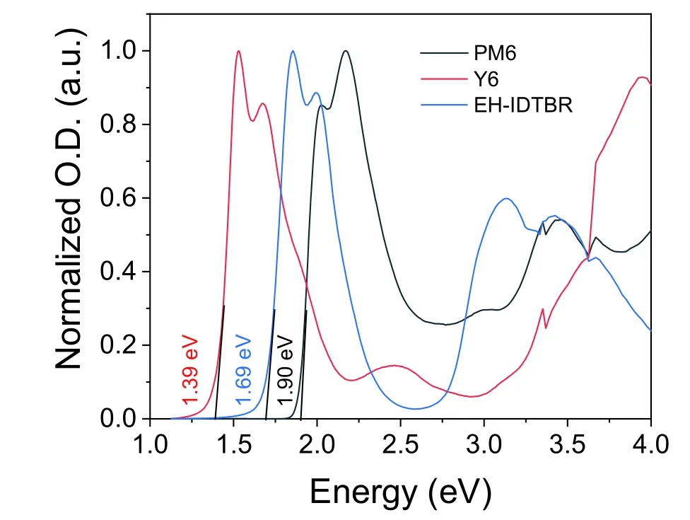
Fig.S1.Tauc plots for PM6,Y6 and EH-IDTBR films.
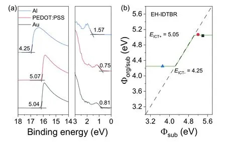
Fig.S2.(a) UPS spectra of EH-IDTBR film on different substrates.(b) Energies of ICT states of EH-IDTBR film.
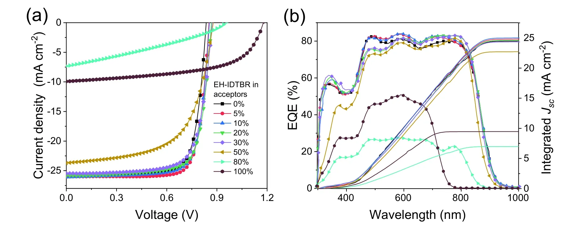
Fig.S3.(Color online) (a) J–V curves of ternary cells with different EH-IDTBR contents;(b) the corresponding EQE curves.


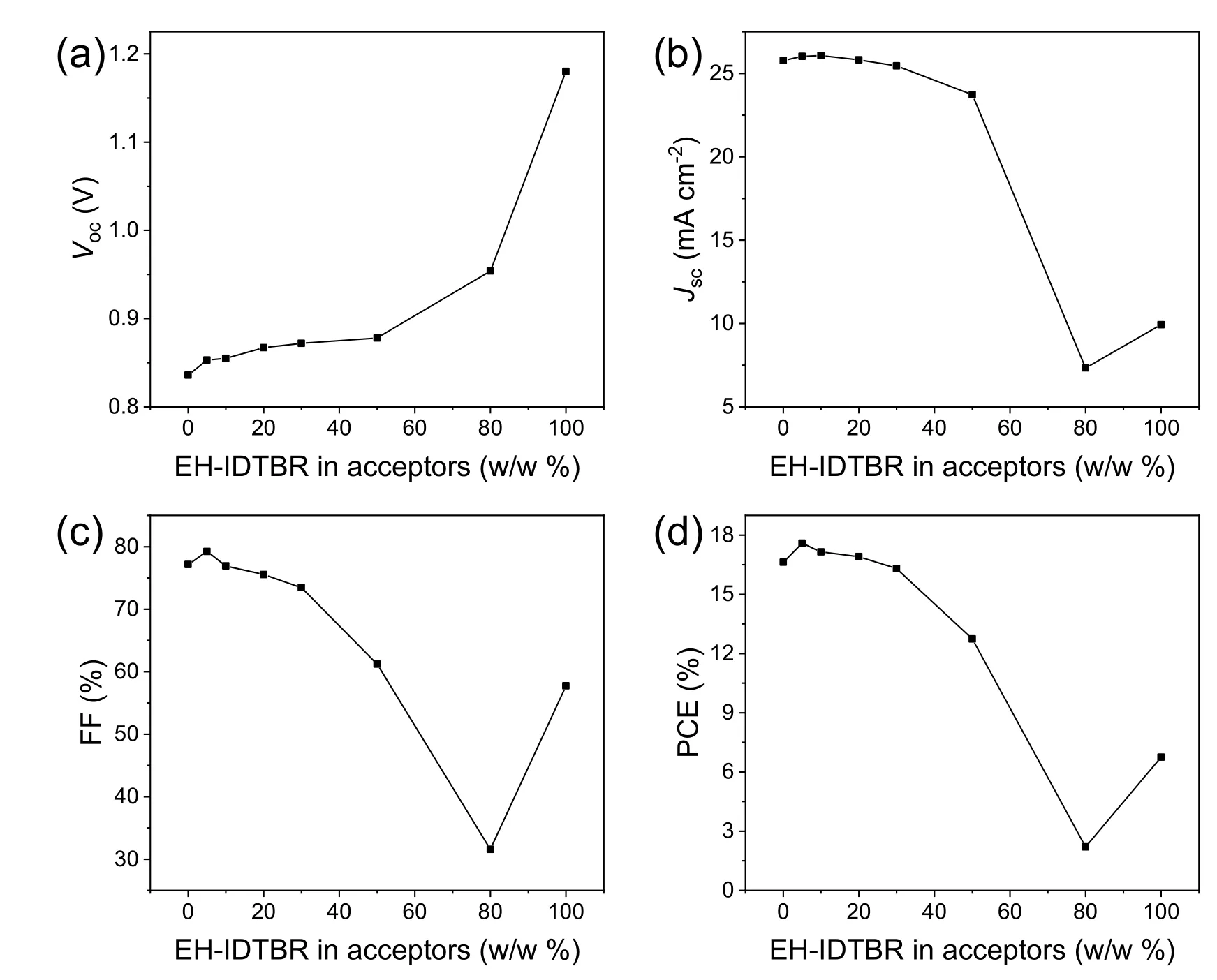
Fig.S4.(a) Voc,(b) Jsc,(c) FF and (d) PCE of the ternary cells with different EH-IDTBR contents.
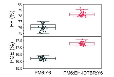
Fig.S5.FF and PCE distribution for PM6:Y6 and PM6:EH-IDTBR:Y6 cells.
whereTwas absolute temperature,kBwas Boltzmann’s constant andErepresented photon energy.For the fit parameters,ECTrepresented the free-energy difference between the charge transfer complex (CTC) ground state and the CT excited state,andECTenergy can be quantified by the point of intersection between CT absorption and emission.λwas the reorganization energy associated with the CT absorption process,andfwas a measure of the strength of the donor–acceptor coupling.
The total loss can be divided into charge extraction (EgtoECT) and recombination (ECTtoVOC) losses.The recombination losses can be quantified using Eq.(S14),including the contribution of radiative (ΔVrad) and non-radiative losses(ΔVnon-rad).Employing the Marcus fitting parametersf,λ,andECT,which are extracted from Fig.1(g) and Fig.S24 and summarized in Table S6,the ΔVradcan be quantified using Eq.(S15).ΔVnoradcan be directly evaluated according Eq.(S16) by EQEELmeasurements.The calculated value of ΔVradand ΔVnon-radfor all our devices can be seen in Table S7.Consequently,the total energy loss followed the expression in Eq.(S17).
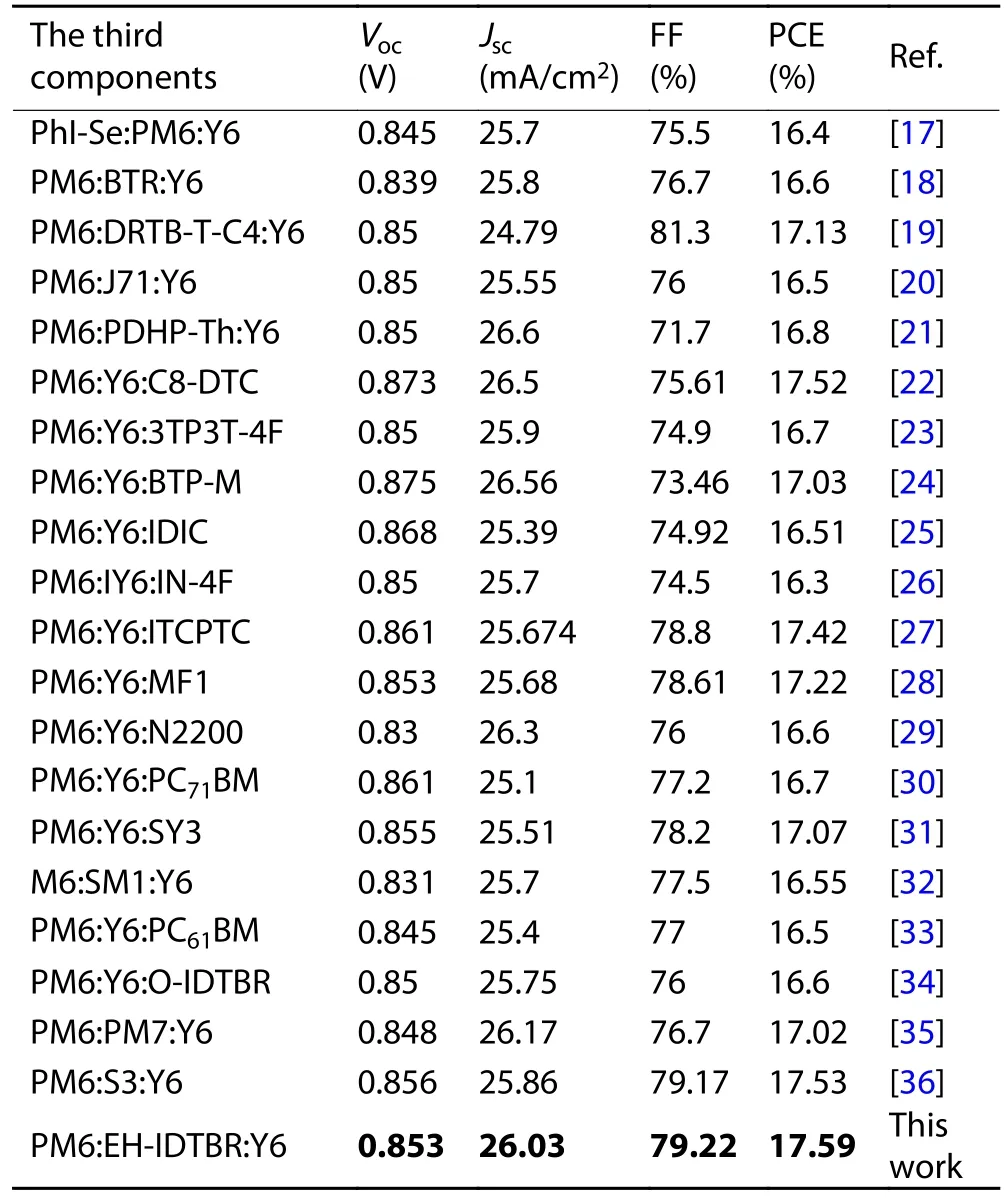
Table S1.Photovoltaic parameters of PM6:Y6-based ternary OSCs.
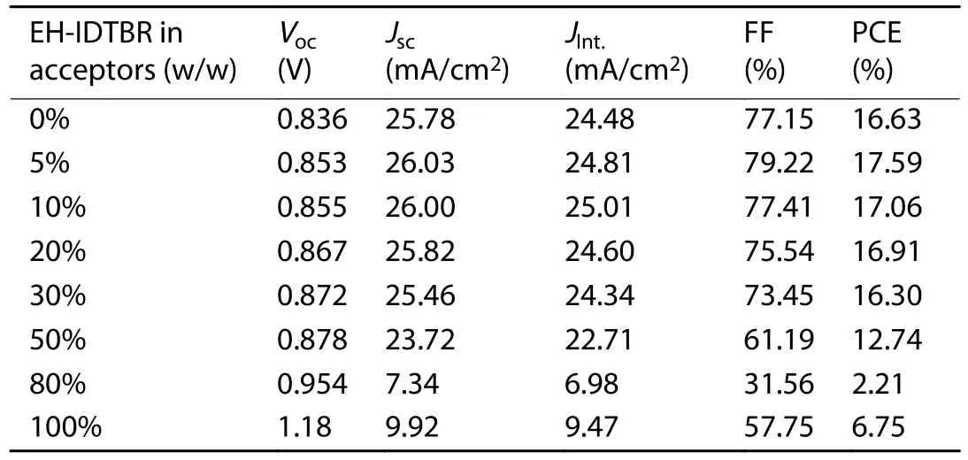
Table S2.Photovoltaic parameters of the cells with different EH-IDTBR contents.

Table S3.Parameters from the Jph–Veff plots.
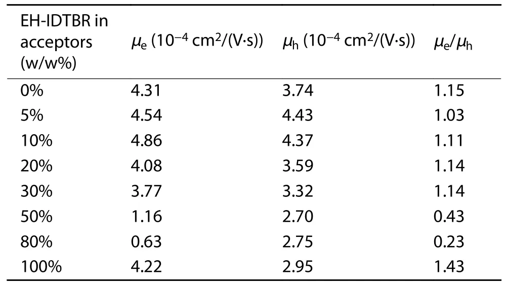
Table S4.Electron and hole mobilities of the blend films with different EH-IDTBR contents.

Table S5.GIWAXS parameters.

Table S6.The parameters used to calculate energy loss.

Table S7.Energy loss details.
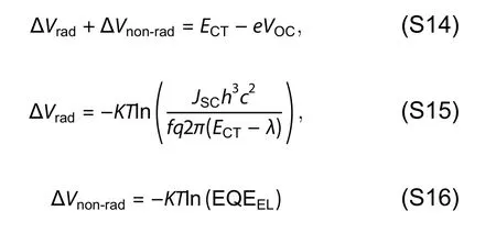
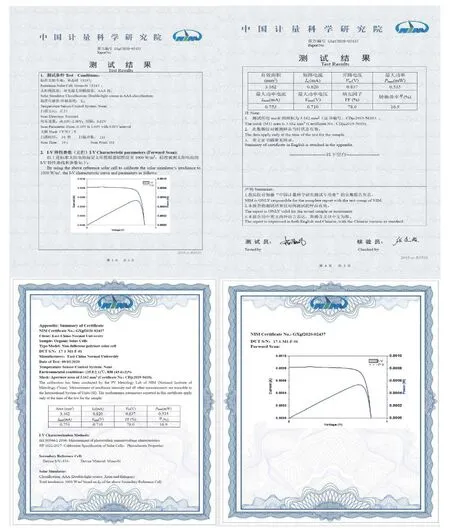
Fig.S6.(Color online) NIM (Beijing) report for PM6:EH-IDTBR:Y6 cells.(Voc:0.837 V,Jsc:25.93 mA/cm2,FF:78%,PCE:16.9%)

Morphology characterization
Atomic force microscopy (AFM) measurements were carried out in the tapping mode (Mutimode 8,Bruker) at ambient condition.Transmission electron microscope (TEM) measurements were conducted with a JEM-2100F microscope operated at 150 K.GIWAXS measurements were accomplished with a Xeuss 2.0 SAXS/WAXS laboratory beamline using a Cu X-ray source (8.05 keV,1.54 Å) and a Pilatus3R 300K detector.The incidence angle is 0.2°.The parameters of π–π stacking distance (d-spacing) and the crystal size of the domains can be estimated by crystal coherence length (CCL),according to the Scherrer equation[2]:

Here,qis the location of the peak and FWHM is the halfwidth at the diffraction peak.

Fig.S7.(a) PL spectra of neat and blend films.(b) Enlarged PL spectra of blend films.
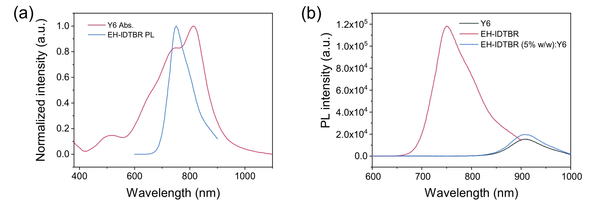
Fig.S8.(a) UV–vis absorption spectrum of Y6 and PL spectrum of EH-IDTBR.(b) PL spectra of Y6,EH-IDTBR and EH-IDTBR (5% w/w):Y6 films.
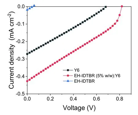
Fig.S9.J–V curves of the cells with Y6,EH-IDTBR and EH-IDTBR (5% w/w):Y6 as active layers,respectively.
Femtosecond (fs) transient absorption (TA) spectroscopy therefore is employed to probe the hole transfer dynamics in the ternary and reference binary blends.A 725 nm wavelength laser is applied to selectively excite the acceptors without pumping the donor.For the acceptor films,the bleach peaks mainly appear at 830 nm for Y6 and EH-IDTBR(5% w/w):Y6,680 nm for EH-IDTBR (Fig.S10),corresponding to the ground state bleach (GSB) and stimulated emission(SE) of the absorption transition in the acceptors after photoexcitation[3,4].Figs.S11(a) and S11(b) display the 2D color plot and a few representative TA spectra for the ternary PM6:EHIDTBR (5% w/w):Y6 film,respectively.The main bleach signals at 650-850 nm appear from the EH-IDTBR (5% w/w):Y6.With the decay of the EH-IDTBR (5% w/w):Y6 bleach peaks,a few clear bleach peaks emerge at 550–610 nm,which match well with the absorption features of PM6.These GSBs in the donor rise with the bleach decay process in the acceptors(Fig.S11(c)),confirming the effective hole transfer process at the donor/acceptor interface[5,6].The similar TA spectra and hole transfer process can be observed in the reference two binary PM6:Y6 and PM6:EH-IDTBR blends (Fig.S12).As shown in Fig.S11(d) and Fig.S12(f),we select the representative kinetics wavelength where the acceptors show no TA signal (Fig.S10) to monitor rising kinetics of PM6.The hole-transfer rates are fitted with bi-exponential functions with time constants ofτ1,h=119 fs andτ2,h=13.11 ps for the PM6:Y6 blend.The former represents the ultrafast exciton dissociation at the donor/acceptor interface,while the latter is assigned to the exciton diffusion time towards interface before dissociation[5,7].As a contrast,the ternary blend exhibits the faster transfer rate with time constants ofτ1,h=88 fs andτ2,h=10.41 ps.The trend in the hole transfer rate is consistent with the values of HOMO offsets.Introducing EH-IDTBR into the PM6:Y6 blend increases the size of the donor/acceptor HOMO offset,leading to the enhanced driving force with the faster hole transfer,contributing to the enhancedJscand FF in the ternary OSCs.Although the PM6:EH-IDTBR blend has the largest HOMO offset with the fastest hole transfer speed (Fig.S12(f)),the signal intensity rapidly decreases from 10 to 100 ps,which signifies the sharp recombination process and thus results in the poor device performance.
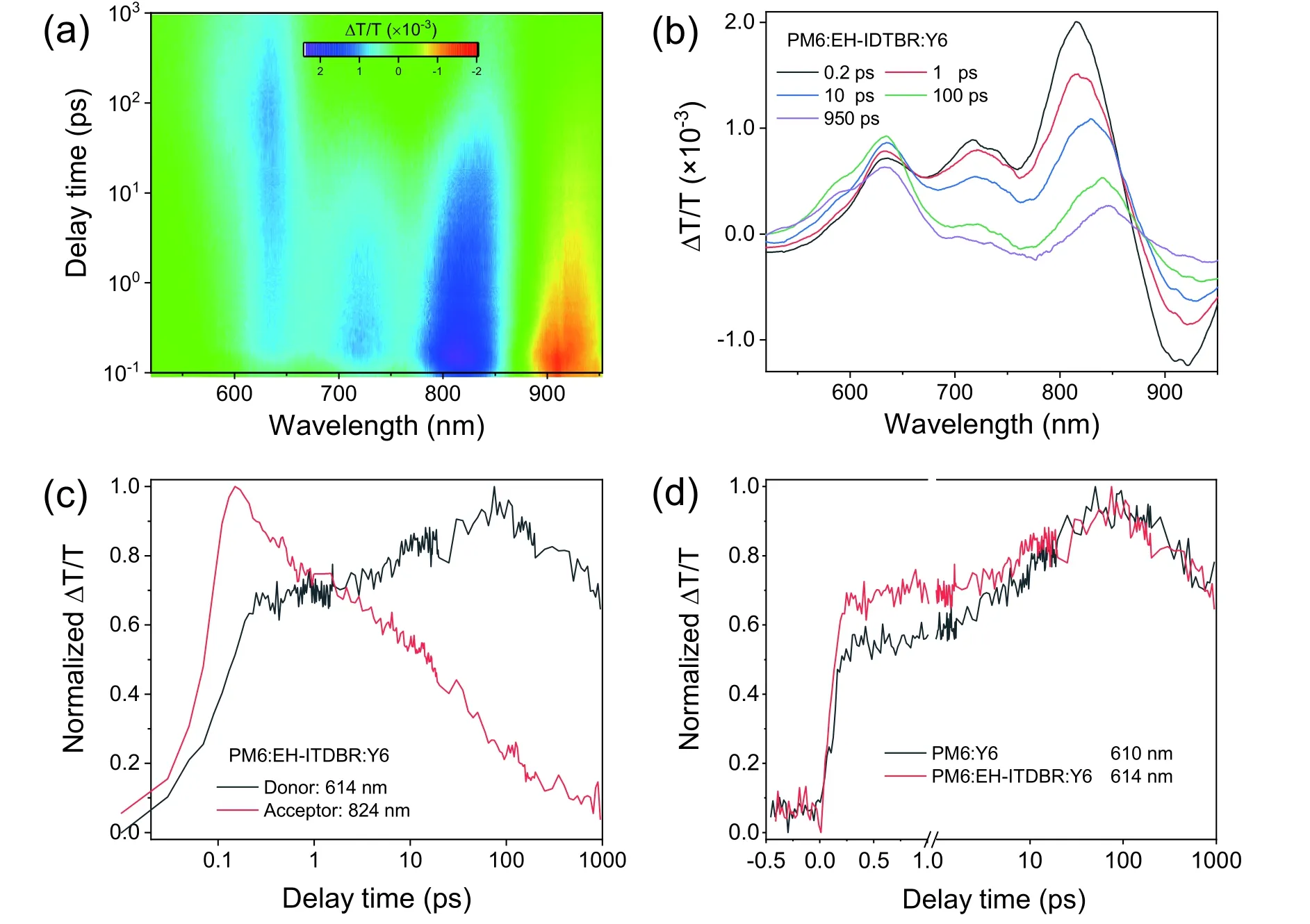
Fig.S11.(Color online) (a) 2D color plots of fs TA spectra for PM6:EH-IDTBR:Y6 blend film at under 725 nm excitation with a fluence below 10 μJ/cm2.(b) Representative fs TA spectra at indicated delay times.(c) TA hole transfer kinetics in PM6:EH-IDTBR:Y6.(d) Comparison of the hole transfer kinetics for PM6:Y6 (black line) and PM6:EH-IDTBR:Y6 (red line).
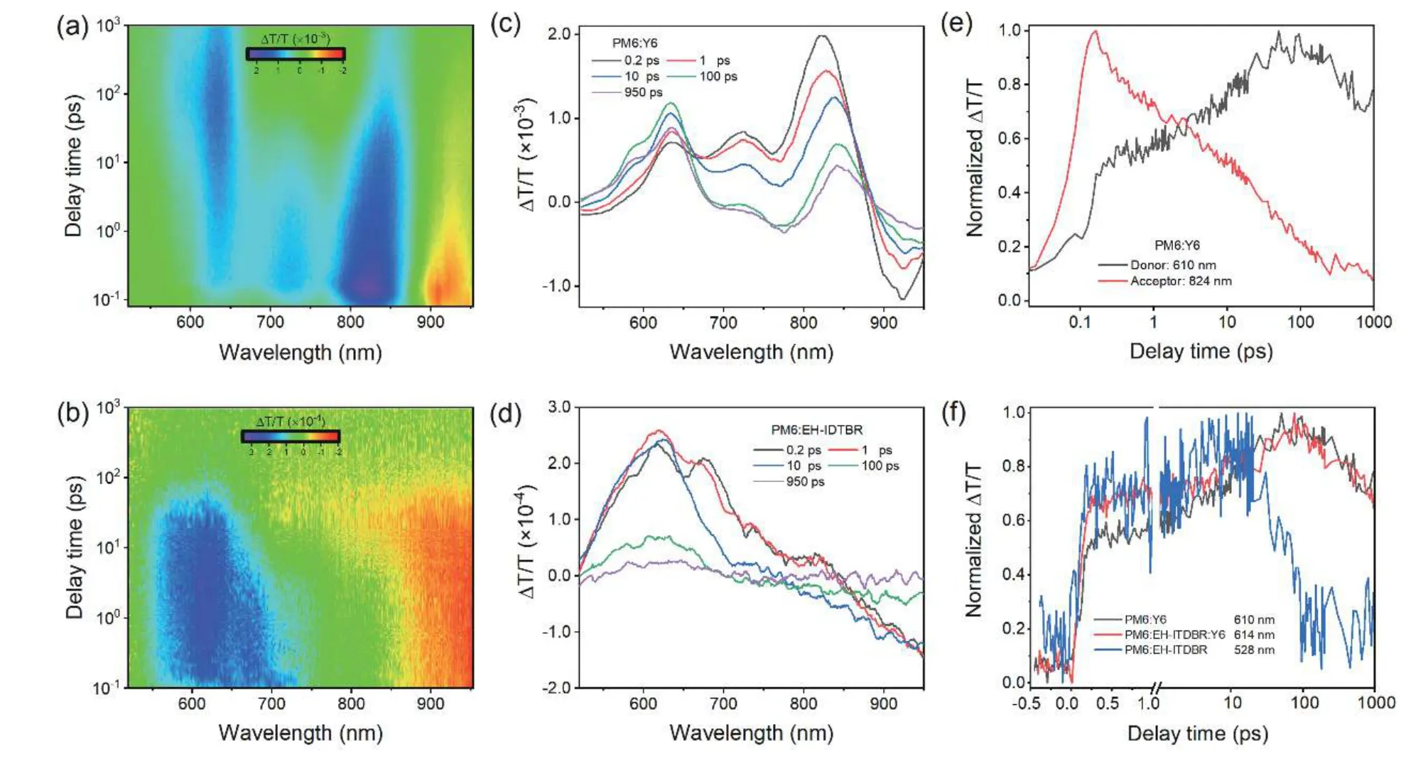
Fig.S12.(Color online) 2D color plots of fs TA spectra for (a) PM6:Y6 and (b) PM6:EH-IDTBR blend films under 725 nm excitation;representative fs TA spectra of (c) PM6:Y6 and (d) PM6:EH-IDTBR films at indicated delay times;(e) TA hole transfer kinetics in PM6:Y6 showing the hole transfer process;(f) comparison of the hole transfer kinetics for PM6:Y6 (black line),PM6:EH-IDTBR:Y6 (red line) and PM6:EH-IDTBR (blue line).
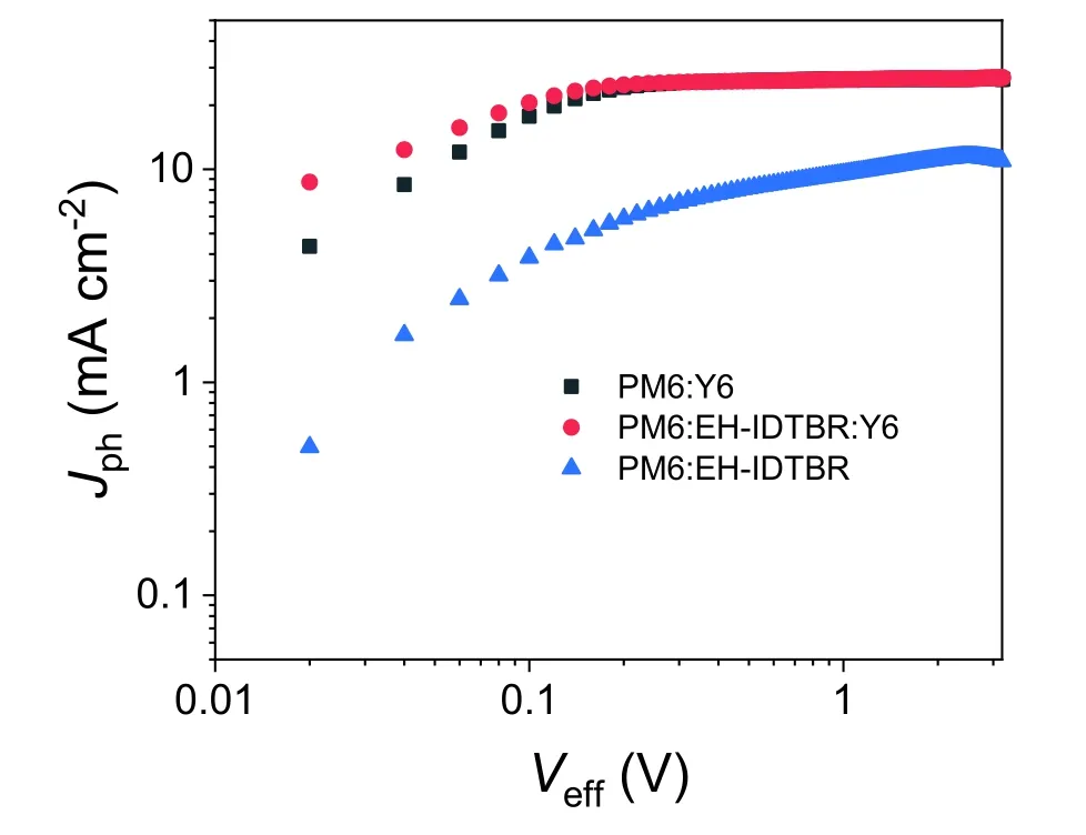
Fig.S13.Jph–Veff plots for PM6:Y6,PM6:EH-IDTBR and PM6:EH-IDTBR:Y6 cells.

Fig.S14.(Color online) J–V curves of PM6:Y6,PM6:EH-IDTBR:Y6 and PM6:EH-IDTBR cells under different illumination intensities.
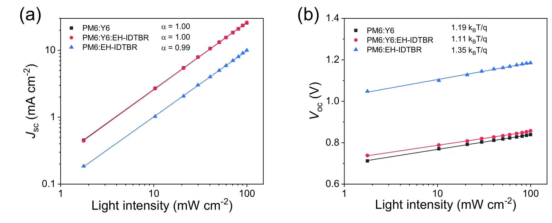
Fig.S15.(a) Jsc–Plight and (b) Voc–Plight plots for PM6:Y6,PM6:EH-IDTBR:Y6 and PM6:EH-IDTBR cells.
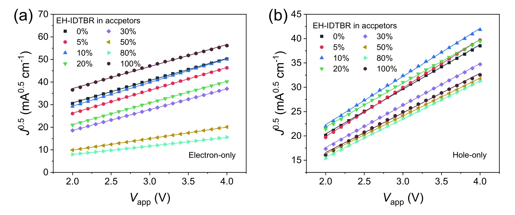
Fig.S16.J0.5–Vapp plots for (a) the electron-only devices with a structure of ITO/ZnO/active layer/PFN-Br/Ag and (b) the hole-only devices with the structure of ITO/PEDOT:PSS/active layer/Au.
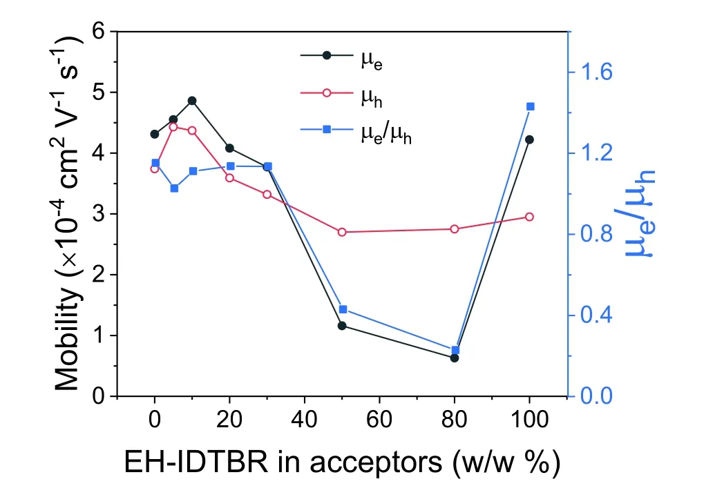
Fig.S17.The variation of μe,μh and μe/μh along with EH-IDTBR contents.
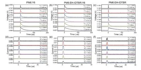
Fig.S18.(a–c) TPV and (d–f) TPC spectra for PM6:Y6,PM6:EH-IDTBR:Y6 and PM6:EH-IDTBR cells under different light intensities.
The charge carrier lifetime (τ) is derived from TPV that corresponds to the differentVoc(Figs.S18(a)–S18(c)) by mono-exponential fitting of TPV decay and shows the linear dependence onVocin semi-log plot[8,9](Fig.S19(a)).We find that the introduction of EH-IDTBR (5% w/w) yields a longer lifetime(τ=6.54μs) under 1 sun illumination compared with the binary devices (τ=3.46μs for PM6:Y6,andτ=1.46μs for PM6:EH-IDTBR).The charge carrier density (n) is extracted from the differential capacitance approximation based on both TPC and TPV results[10,11](Described in Experimental section,and Figs.S18(d)–S18(f)).Besides,the devices follow a power law:τ=τ0n–λ(whereτ0is the constant,λ represents the recombination exponent)[12,13].A recombination orderR=λ+1 equal to 2 suggests dominant biomolecular recombination process[12].TheRof 1.99 for the optimal ternary device means nearly an ideal (trap-free) bimolecular recombination,justified by the high FF of 79.22%.The R greater than 2 is normally attributed to the effect of trap-assisted recombination.For binary PM6:Y6 and PM6:EH-IDTBR devices,theRare 2.06 and 2.35,respectively,in line with the results of steadystate dependence ofVocon light density (Fig.1(f)).The nongeminate recombination rate coefficient (Knge) is defined by 1/τ(n)n(whereτ(n)is the charger carrier lifetime under corresponding density)[8,10].As shown in Fig.S19(d),the ternary device has the lowestKngeof 1.14 × 10⁻¹⁷m3/s,confirming the suppressed recombination.AsKngeand charge mobility follow the same dependence on n,the Langevin recombination rate coefficient (KL) can be assessed by.TheKLfor the ternary and PM6:Y6 binary are 5.41 × 10⁻¹⁶and 4.86 ×10⁻¹⁶m3/s,respectively,as included in Fig.S19(d) for comparison.TheKngeof the optimized ternary device is smaller than theKL,indicating significantly reduced non-geminate recombination loss.
The root-mean-square roughnesses are slightly varied,indicating that EH-IDTBR is finely mixed with the host PM6:Y6 blend.As seen from their phases images,the PM6:EH-IDTBR(5% w/w):Y6 blend features a uniform fibrillar structure,similar with the PM6:Y6.
TheEgof the blend films calculated by the intersection point of absorption and emission spectra are 1.415,1.416 and 1.721 eV for PM6:Y6,PM6:EH-IDTBR:Y6 and PM6:EH-IDTBR,respectively (Fig.S24).TheECTis determined by fitting the sub-gap absorption of highly sensitive EQE and EL[15].ΔEradis inevitable in the devices,and the ΔEradof the ternary device is close to the host binary PM6:Y6 device since there is no additional gap states after introducing EH-IDTBR.ΔEnon-radis quantified by EQEELmeasurements,expressed as−kTln(EQEEL)[16].
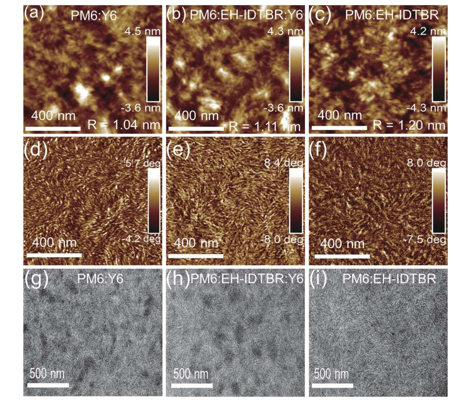
Fig.S20.(Color online) (a–c) AFM height images and (d–f) phase images.(g–i) TEM images.

Fig.S21.(Color online) (a–h) AFM height images and (i–p) phase images for the blend films with different EH-IDTBR contents.
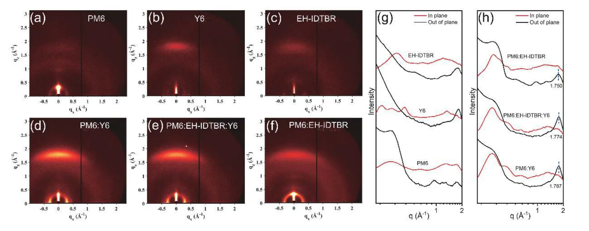
Fig.S22.(Color online) (a–f) 2D GIWAXS patterns of the neat,binary and ternary films.(g–h) In-plane (red) and out-of-plane (black) profiles of the 2D data.
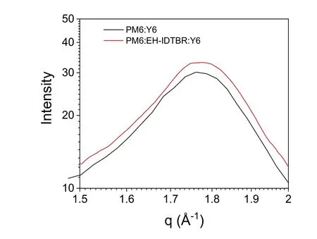
Fig.S23.Enlarged out-of-plane profiles of PM6:Y6 and PM6:EH-IDTBR:Y6 of the 2D data.
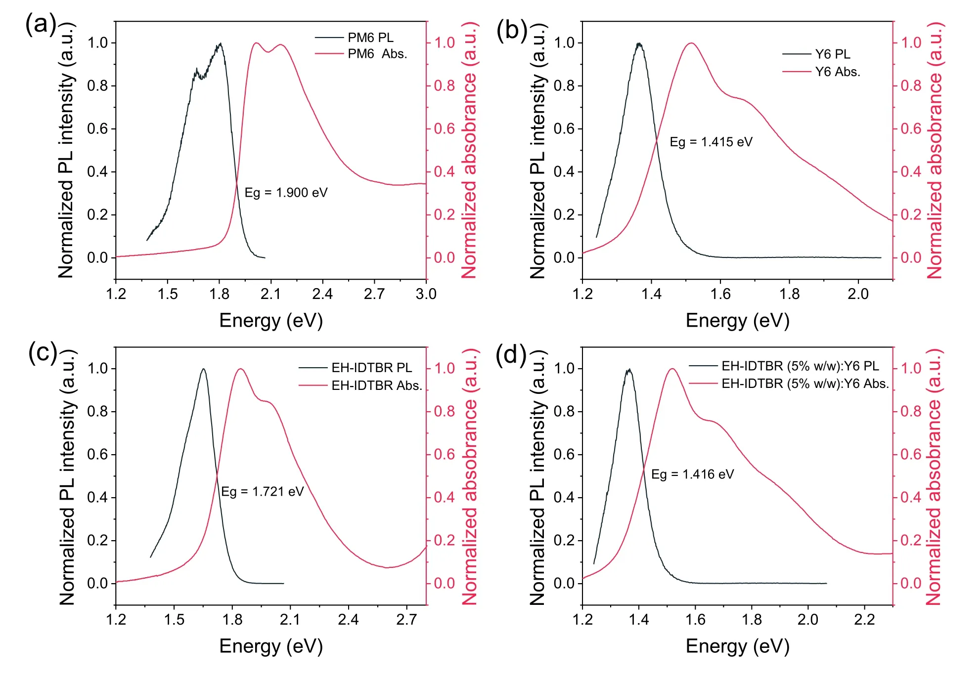
Fig.S24.PL and UV–vis spectra for (a) PM6,(b) Y6,(c) EH-IDTBR and (d) EH-IDTBR (5% w/w):Y6 films.
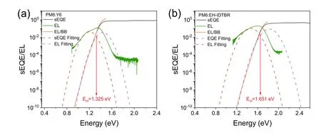
Fig.S25.sEQE and EL spectra for (a) PM6:Y6 and (b) PM6:EH-IDTBR cells.
 Journal of Semiconductors2021年9期
- Journal of Semiconductors的其它文章
- Organic semiconductors:commercialization and market
- Self-assembled monolayers in perovskite solar cells
- 2D transition metal dichalcogenides for neuromorphic vision system
- Chip-based quantum communications
- Synthesis of two-dimensional/one-dimensional heterostructures with tunable width
- The scanning tunneling microscopy and spectroscopy of GaSb1–xBix films ofa few-nanometer thickness grown by molecularbeam epitaxy
