Organic semiconductors:commercialization and market
Xi Yang and Liming Ding
1ChasingLight Technology Co.,Ltd,Guangzhou 510700,China
2Center for Excellence in Nanoscience (CAS),Key Laboratory of Nanosystem and Hierarchical Fabrication (CAS),National Center for Nanoscience and Technology,Beijing 100190,China
3School of Materials and Energy,Guangdong University of Technology,Guangzhou 510006,China
Organic semiconductors (OS) have a number of advantages over their inorganic counterparts,e.g.,mechanical flexibility,lightweight,solution processability,and low-cost highthroughput production.Moreover,thanks to the versatility of synthetic organic chemistry,the optoelectronic properties of OS can be tuned readily on demand.They can be incorporated into a wide range of applications from biomedical sensors,image sensors,flexible microprocessors,photovoltaics to flexible displays,etc.In the field of wearable electronics and Internet-of-Things,there is an increasing demand for smart and unobtrusive sensors that can be adhered onto curved surfaces or interfaced with human body[1].In such cases,the rigidity and heavy weight of traditional inorganic semiconductors will certainly become a limitation,while OS will become alternatives,standing on their rapidly improved performance.In fact,ever since the first demonstration of thin-film organic solar cell and light-emitting diode in late 1980s,research on OS has been pushing these novel semiconducting technologies into commercialization[2].
Organic light-emitting diode (OLED) is the first successfully commercialized OS technology.Owing to the thinness,better flexibility,lower energy consumption,wider viewing angle,faster response speed and higher color gamut,OLED displays are regarded as the next-generation display technology to replace liquid-crystal displays (LCD)[3].To date,OLED displays are becoming the mainstream mid-to-high-end display technology in small and medium-sized applications such as mobile phones and smart watches.In 2021,the market share of OLED mobile phones will reach~40%.At present,small and medium-sized OLED panels,usually from G6 line(substrate size:1500 × 1850 mm2),use the RGB evaporation process.It is difficult to apply such evaporation technology to produce large-size display panel (usually >G8.5 line,substrate size:2200 × 2500 mm2) due to the fine metal mask(FMM) problems.With the maturity of large-size panel processese.g.,printed display and QD-OLED technology,and with the continuous decline in fabrication costs,it is expected that OLED technology will take over large-size display market within 5 years.
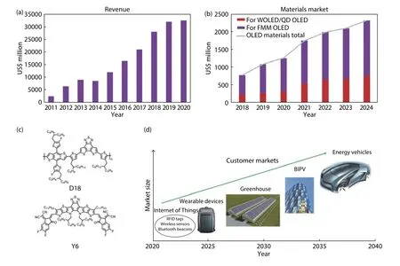
UBI Research's latest report[4]indicates that global OLED panel shipments in 2020 accomplished 577.88 million units,with a year-on-year increase of 3.7%.The total revenue of OLED panels for the year increased by 0.7% and reached 32.68 billion USD (Fig.1).The top three manufacturersi.e.,SAMSUNG,LGD and BOE,account for 95% of the overall global OLED share.The whole display market is accelerating its shift to mainland China,which may surpass South Korea to become the world's largest display country within 3–5 years.At present,there are more than 20 OLED production lines running and under construction in China,with a total investment of >500 billion RMB.Taking the mobile phone as an example,the market share for China’s OLED panel makers was increased to 88 million shipments in 2020,standing for a yearon-year increase of 60%,and China in this area took almost 20% of the market share.
OLED materials are the core of OLED display technology and account for~20% of the panels cost.In 2020,the global OLED materials revenue reached 1.259 billion USD,with a year-on-year increase of 16%.It is estimated that in 2021,the global OLED materials revenue will get to 1.754 billion USD,with a 40% year-on-year growth.In particular,regarding the bottlenecks for key materials development,in the past,China’s material manufacturers usually engaged in the processing and production of materials intermediates with low technical content and low profits.Most of domestic OLED materials are still dependent on imports,especially emissive materials with high technical barriers.For example,red and green emissive materials are still monopolized by UDC (USA),and blue ones mainly come from Idemitsu in Japan and SFC in South Korea.Especially in South Korea,as SAMSUNG and LG play a leading role in the entire display industry chain,a large number of materials companies have risen rapidly,occupying more and more market shares.Fortunately,this situation is changing recently.In the past two years,with the massive investment in research and development,China OLED materials have begun to gradually promote the localization of transmission layer materials,and many materials have been verified in the panel factory or are in the process of implantation.
Right now,in terms of the industrialization of OLED materials,red and green emissive materials still use Ir-complex based phosphorescent emission,and blue ones use fluorescent emission.The phosphorescent host currently adopts the concept of organic alloy proposed by SDI,which can form a co-host premix of exciplex.The fluorescent host adopts the TTA approach (triplet-triplet annihilation) to improve the internal quantum efficiency.Meanwhile,new molecules and luminescence mechanisms are constantly being developed,such as TADF,TADF-based hyperfluorescence,and radicalbased doublet emission[5−7].It is worth noting that since last year,the B-N based TADF blue emitters,proposed by Kwansei Gakuin University and JNC of Japan,have been introduced into the panel line.This marks that the third-generation OLEDs are now moving to commercialization after fluorescence and phosphorescence.

Fig.1.(Color online) (a) OLED panel revenue from UBI Research[4].(b) OLED materials revenue from UBI Research[4].(c) Chemical structure of D18[11] and Y6[10].(d) Customer markets for OPV.
Organic photovoltaic (OPV) is considered to be the second OS technology to be commercialized after OLED.OPV has the advantages of solution processability,flexibility,semitransparency,colorfulness,high efficiency,and low cost.Therefore,it represents one of the most promising photovoltaic technology that can be applied to Internet-of-Things equipment,building photovoltaic integration,and wearable electronic device.
For a long time,fullerene derivatives have been used as the acceptor materials in OPV[8,9],however,they offer low efficiency.In 2019,Zouet al.developed A-D-A type small molecule Y6,which now becomes one of the most popular nonfullerene acceptors[10].After that,scientists focus on Y6 derivatives,boosting OPV efficiency rapidly in last few years.Dinget al.have developed D18 series polymer donors,pushing the efficiency to over 18%[11,12].The efficiency for the 204 cm2solar module has reached 11.73%[13].We believe that the efficiency and lifetime for current OPV modules already meet the needs of some commercial applications.The future development direction of OPV technology will not be to compete with crystalline silicon photovoltaics,but to coexist.Considering the carbon-neutrality strategy,crystalline silicon photovoltaics will be connected to the grid at a fair price.OPV can find applications that cannot be realized by crystalline silicon photovoltaics,e.g.,weak-light,indoor-light,flexible and semitransparent applications[14,15].It is foreseeable that the most ideal commercialization in next five years will be to power low-power electronic devices such as the Internet-of-Things,wearable devices or smart homes.After 5–10 years,when the stability and cost issues are resolved,OPV will be further applied to BIPV,smart greenhouses,and new energy vehicles.
The next ten years will be a critical stage for the development of OS technology.We believe China shall not only solve the existing bottleneck issues,but also take the lead in the commercialization of OS technologies.The very important strategies are as follows:For OLED,(1) accelerating the development of self-patented OLED materials and equipments to break patent monopoly;(2) actively laying out a new generation of printing display,including soluble materials,printing equipments and printing processes,to occupy a position in the competitive market of large-size displays.For OPV,(1) using the technical advantages of domestic scientists to quickly intervene and promote OPV industrialization;(2) making a sound patent layout early and lead the development of the global OPV industry;(3) correctly choosing the application direction of OPV technology to keep in touch with downstream application requirements,and to seek a rational commercial application model;(4) strengthen cooperation between different R & D teams,as well as between academics and industries,to form domestic OPV agglomeration advantages and promote the development of China’s OPV industry.
Besides the two leading technologies,OLED and OPV,other technologies like organic photodetectors (OPD) and organic transistors (OFET) will also find their opportunities for commercialization[16,17].With the experience of OLED industrialization,the commercialization of other OS devices will be greatly accelerated.We believe that OS technologies will find broad applications in our life in the near future.
Acknowledgements
We thank the National Key Research and Development Program of China (2017YFA0206600) and the National Natural Science Foundation of China (22005062,51773045,21772030,51922032 and 21961160720) for financial support.
 Journal of Semiconductors2021年9期
- Journal of Semiconductors的其它文章
- Self-assembled monolayers in perovskite solar cells
- 2D transition metal dichalcogenides for neuromorphic vision system
- Investigating the reason for high FF from ternary organic solar cells
- Chip-based quantum communications
- Synthesis of two-dimensional/one-dimensional heterostructures with tunable width
- The scanning tunneling microscopy and spectroscopy of GaSb1–xBix films ofa few-nanometer thickness grown by molecularbeam epitaxy
