Targeted transfer of self-assembled CdSe nanoplatelet film onto WS2 flakes to construct hybrid heterostructures
Zeguo Song, Yunkun Wang, Yunke Zhu, Peng Bai, An Hu, and Yunan Gao,
1State Key Laboratory for Artificial Microstructure and Mesoscopic Physics, School of Physics, Peking University, Beijing 100871, China
2Frontiers Science Center for Nano-optoelectronics, Beijing 100871, China
3Collaborative Innovation Center of Extreme Optics, Shanxi University, Taiyuan 030006, China
Abstract: Colloidal CdSe nanoplatelets are thin semiconductor materials with atomic flatness surfaces and one-dimensional strong quantum confinement, and hence they own very narrow and anisotropic emission.Here, we present a polydimethylsiloxane (PDMS) assisted transferring method that can pick up single layer CdSe nanoplatelet films self-assembled on a liquid surface and then precisely transfer to a target.By layer-by-layer picking up and transferring, multiple layers of CdSe films can be built up to form CdSe stacks with each single layer having dominant in-plane transition dipole distribution, which both material and energic structures are analogous to traditional multiple quantum wells grown by molecular-beam epitaxy.Additionally,with the great flexibility of colloidal nanoplatelets and this transferring method, CdSe nanoplatelets films can be combined with other materials to form hybrid heterostructures.We transferred a single-layer CdSe film onto WS2 flakes, and precisely studied the fast energy transfer rate with controlled CdSe nanoplatelet orientation and by using a streak camera with a ps time resolution.
Key words: CdSe nanoplatelets; self-assembly; transfer; energy transfer; hybrid heterostructures; WS2
1.Introduction
Colloidal semiconductor nanocrystals have been intensively studied for several decades, and various types in chemical compositions, shapes and sizes can be synthesized[1].CdSe nanoplatelets, as one type of nanocrystal with an anisotropic shape, attracted increasing interest in recent years, because they have very sharp emission peaks and pure in-plane transition dipoles[2−4].They are very promising for developing lowcost and highly efficient nanocrystal-based light emitting diodes and lasers[5−9].
For controlling these nanocrystals to build macro-scale functional materials, self-assembly of them has been considered as the most promising method[10−14].Several groups have used liquid surface self-assembly to successfully have CdSe nanoplatelet oriented in either face-down or side-up configuration[2,15−17].For further property studies and applications, the self-assembled films need to transfer on solid substrates.Typically, it was achieved by submerging the targeted substrate into the supporting liquid and then draining the liquid away[2,15,17].This strategy, although workable, has several drawbacks as that the targeted samples have to be stable against the supporting liquid and should have sufficient size to avoid misalignment.Baiet al.used ink-jet printing to directly assemble nanoplatelets to uniform films with a size of tens of micrometers on a number of substrates[18].For this method, the surface properties of the targets have to be properly controlled to allow the nanoplatelet to assemble during the drying process.While controllable self-assembly of nanocrystals has achieved significant progress, transferring methods are not yet well developed.
In this work, we report a fascinate method that can pick up the self-assembled single-layer CdSe films suspended on acetonitrile and then precisely transfer onto targeted substrates.Combining transmission electron microscopy (TEM),atomic force microscopy (AFM) and back focal plane imaging (BFP), we determined that the films exhibit an around 90% in-plane transition dipole distribution.Using this method, it is very convenient to construct hybrid heterostructure combining colloidal quantum dots with other structures and/or materials, in which new properties can be exploited[19−24].Herein, we transferred a single-layer CdSe film onto a WS2flake.With the controlled nanoplatelet orientation and using ps time-resolved streak camera, the energy transfer rate between these two types of two-dimensional materials is precisely determined.
2.Methods
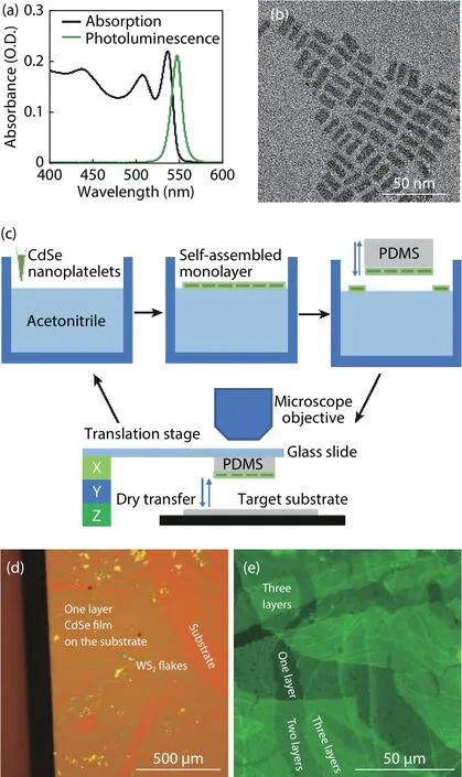
CdSe nanoplatelets were synthesized following Ref.[25],and the absorption and photoluminescence spectra are presented in Fig.1(a).A TEM image of these nanoplatelets all laying face-down on a TEM grid is presented in Fig.1(b), from which the length and width are determined to be 18 × 5 nm2.The thickness of the nanoplatelets is 1.5 nm, which has been well documented in literature for CdSe nanoplatelets with the emission peak at 550 nm[25].Fig.1(c) illustrates the PDMS-assistedtransferring method.Self-assembly of the CdSe nanoplatelet single layer was carried out by adding a small amount of CdSe nanoplatelets dispersed in hexane on top of acetonitrile.After the hexane evaporated, a single layer of the nanoplatelet film was left on the acetonitrile surface.A PDMS stamp was bought close to the surface slowly using a motorized translation stage to pick up the film.For transferring, the PDMS stamp was mounted on a glass slide.Monitored in microscopy, the stamp was brought close to the target substrate slowly by a motorized translation stage.Fig.1(d) shows a bright-field microscopy image of a layer of CdSe nanoplatelets transferred on a SiO2/Si substrate with WS2flakes mechanically exfoliated in advance.Multilayer films could be built up by repeating the whole process described above with the substrate heated up to 85 °C by a hotplate, hold for 30 s and cooled down quickly by a water chiller.Fig.1(e) shows a photoluminescence image of nanoplatelet films on a cover glass substrate with one, two and three layers of CdSe nanoplatelets in different areas.Shortly heating the CdSe nanoplatelet films at a moderate temperature of 85 °C did not decrease their photoluminescence brightness.We noticed that the nanoplatelet film could be directly transferred on a glass substrate at room temperature while the subsequent transfers required a raised temperature.The relative strengths of the interface interaction between substrate/nanoplatelets, nanoplatelets/nanoplatelets, and nanoplatelet/PDMS, determine whether the nanoplatelet film can be transferred onto the target.Increasing the temperature decreases the viscosity of PDMS and helps to release the CdSe nanoplatelet films.

Fig.1.(Color online) (a) Absorption and photoluminescence spectra of the CdSe nanoplatelets.(b) Transmission electron microscopy(TEM) image of the nanoplatelets.(c) Schematic of PDMS assisted transferring method.(d) A bright-field microscopy image of a single layer of the CdSe nanoplatelet film on a SiO2/Si substrate with WS2 flakes.(e) Photoluminescence microscopy image of CdSe films with one, two and three layers of nanoplatelets.
Atomic force microscopy (AFM) images were measured by an Oxford Cypher ES AFM.Back focal plane images were collected with the same instrument in our previous work of Ref.[18].Time resolve photoluminescence spectra were collected by a streak camera (Hamamatsu C5680-04).The samples were excited at 415 nm under 3.8 MHz by using a 76 MHz femtosecond Ti:sapphire oscillator (fundamental 830 nm and frequency-doubled by a BBO crystal to 415 nm, and the repetition frequency lowered by a pulse picker).The laser spot is about 1μm in diameter.Photoluminescent signals were filtered by a 450 nm long pass filter to separate the emission of the nanoplatelets from the excitation light.The photoluminescent emission images were taken by a CCD camera in a microscopy under excitation of a 395 nm LED lamp.TEM images were collected by a FEI Tecnai T20 with an accelerating voltage of 200 kV.
3.Results and discussion
Fig.2 shows a photoluminescence microscopy image of a CdSe nanoplatelet film successfully transferred on a cover glass, which reaches an area of larger than 7 mm2.Although there are brighter stripes, it can be easily found in areas with lengths and widths of several hundreds of micrometers which show even brightness meaning a homogenous film.Fig.2(b) shows a TEM image of a film transferred on a SiN window supported on Si.It shows an even contrast through the film together with a particularly selected crack to show the contrast.Scattered voids can be noticed.A TEM image with a higher magnification is presented in Fig.2(c), from which the nanoplatelet orientation can be analyzed.The majority of nanoplatelets have a face-down orientation, while side-up orientation nanoplatelets can be found in scattered spots, as shown in the inset.We calculated the total area of these spots that occupies 13% of the total area.This result agrees with the recent study of Momperet al.that fast evaporation of solvent leads to that CdSe nanoplatelets have face-down orientation on acetonitrile surface[16].Our results additionally show that this simple strategy can conveniently produce homogeneous films with sizes up to several millimeters.With a simple PDMS stamp, these films can be readily picked up and transferred to a targeted substrate.
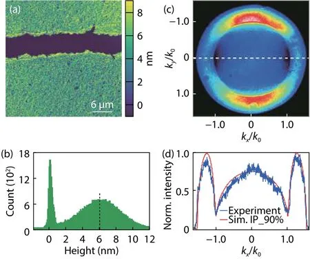
To characterize the film thickness and flatness, an area with a crack was scanned using atomic force microscopy, as shown in Fig.3(a).The image mostly has the same contrast with noticeable scattered darker voids where no nanoplatelets cover the substrate.Similar voids are also noticeable in the results of recent studies where liquid surface assembly was used[2,16].The nanoplatelets on the acetonitrile surface prefers face-down orientation due to the attractive interaction of nanoplatelets ligands and the sub-phase liquids[2,17,26].Edge-to-edge interaction is weak because there arealso fewer ligands on the edge due to their thin thickness,which prevents these nanoplatelets to form a strongly connected and dense film.However, for most applications where multiple layers are needed, these voids can be covered by additional layers and would not be problematic.From the height histogram in Fig.3(b), the average film thickness is 6 nm,which closely equals the total thickness of the nanoplatelets(1.5 nm) and two layers capping ligands (oleic acid of~ 2 nm).Fig.3(b) shows that there is a thickness distribution of 5.6 nm as calculated by the full width at half maximum.This variation partially due the scattered voids mentioned above, and partially due to nanoplatelets with edge-up orientation as have been observed in the TEM image in Fig.2(c).The histogram does show a single peak centered at 6 nm that agrees well with the TEM characterization of a single-layer CdSe nanoplate film with dominant face-down orientation.We have measured the brighter stripes in Fig.2(a) using AFM,and it reveals they are two layers with also the nanoplatelets having the face-down orientation.

Fig.2.(Color online) (a) Photoluminescence microscopy image of a layer CdSe film transferred on a cover glass.(b, c) TEM images of a film on a SiN substrate: (b) panel (lower magnification) shows the homogeneity, and several voids are pointed out by dashed circles; (c) panel (higher magnification) shows that nanoplatelets have dominant in-plane orientation of about 90%, and the inset displayed a zoomed-in portion with nanoplatelets in edge-up (circled in dashed lines) and face-down orientations.

Fig.3.(Color online) (a) AFM image of a CdSe nanoplatelet monolayer film transferred on a cover glass.(b) Height histography of panel a,two peaks correspond to the bare glass and the height of the film.(c) Back focal plane image of the film.(d) Comparison between simulation and experimental BFP results along the dashed crossline in panel c.
Several studies have revealed that these nanoplatelets have pure in-plane dipoles[2,4].Back focal plane imaging(BFP) is a convenient method to characterizing the ensemble transition dipole distributions[2,27].In-plane dipole and outplane dipole show very different image patterns in momentum space, and combined with simulation quantitative results can be drawn.Fig.3(c) presents the BFP image of the monolayer CdSe film transferred on a cover glass.A typical feature from in-pane dipoles of two dark region at |kx| =k0andky= 0 can be clear seen.Quantitative simulation determines that the film has 90% in-plane dipole distribution (Fig.3(d)),which is well in line with the TEM characterization.CdSe nanoplatelets have pure in-plane dipoles, and within the nanoplatelets plane the transition dipoles have no preferred direction[2].Nanoplatelets with edge-up orientation have half inplane and half out-plane transition dipoles.From the TEM analysis, we have calculated that 87% nanoplatelet have in-plane orientation, which have pure in-plane transition dipoles.In the rest, 13% of the nanoplatelets with edge-up configuration transition dipoles are oriented half in-plane and half out of the plane, and hence the total dipoles would have a 93.5%in-plane distribution that agrees well with optical characterization.Using the transferring methods, we have fabricated a sample with three layers of CdSe nanoplatelets films, as shown in Fig.1(e).It gives the same BFP results as the monolayer as expected since each layer is similar.
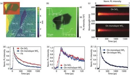
With the controlled nanoplatelet orientation and easily obtained films bigger than hundreds of micrometers, construction of hybrid heterostructures with other materials becomes much more convenient.Herein, we chose WS2flakes as a targeted material as it is one of two-dimensional materials under intensive studies in recent years, and study energy transfer between these two types of two-dimensional materials.In Fig.4(a), the up-left panel shows an optical microscopy image of a WS2flakes consisting different layers, and downright panel presents an AFM image of the constructed heterostructure, where the WS2layer numbers are labeled.The WS2layers were determined by the optical contrast and the thickness is measured by AFM.
Fig.4(b) presents a photoluminescence microscopy image (measured at 550 nm with a band width of 17 nm) of the hybrid heterostructure and the area around with pure singlelayer CdSe nanoplatelet.It clearly shows that with WS2flakes underneath the nanoplatelet film has much lower photoluminescence intensity seen as the darker area.Two insets show the intensity change along the dashed lines.We calculated that monolayer WS2decreases the photoluminescence intensity of the nanoplatelets to 33% while triple-layer to 22% andthe much thicker layer to 7%.This photoluminescence decrease is due to energy transfer from the CdSe nanoplatelet to WS2flakes, since the WS2flakes have a lower energy band gap.Direct charge carrier transfer can be excluded as these CdSe nanoplatelets have capping ligands of oleic acid of about 2 nm length.

Fig.4.(Color online) (a) Up-left panel is an optical microscopy image of WS2 flakes on SiO2/Si, and down-right panel is an AFM image of single-layer CdSe nanoplatelets transferred on the WS2 flakes.(b) Wide field photoluminescence image of the CdSe film on/off the WS2 flakes, and the insets show the intensity change along the dashed white lines.(c) Time- and wavelength-resolved photoluminescence images measured by a streak camera.(d) Integrated intensity decay traces over the emission band in panel c, and biexponential functions are used to fit the decay traces.(e) Similar measurements as in panel c but with a shorter detection window and higher time resolution.(f) Comparison of photoluminescence decay of CdSe nanoplatelets on monolayer and trilayer WS2.
The energy transfer rate in these hybrid heterostructures have been reported with a broad variation in literature[28−31].Federspielet al.reported 5.5 ns–1energy transfer rate from CdSe/CdS/ZnS nanoplatelets to graphene.Taghipouret al.claimed an extremely high rate from CdSe nanoplatelets(emission peak at 510 nm) to monolayer MoS2of 268 ns–1,however the ultrafast process reported in that work is within their instrument response function and the rate was extracted by multiexponential function fitting.By using a streak camera with a ps time-resolution, we can more directedly and accurately measure the energy transfer rate in a similar hybrid heterostructure of CdSe nanoplatelets (emission peak at 550 nm) and WS2flakes.
Fig.4(c) presents two photoluminescence decay images of the nanoplatelet film on bare substrates and on the monolayer WS2region.Clear shortened decay can be seen.The total intensity decay traces over the emission band are shown in Fig.4(d).A biexponential decay function can well fit the decay traces.The fitting extracted two components of with decay time of 53 ± 3 ps and 587 ± 14 ps on the bare substrate while 50 ± 3 ps and 380 ± 8 ps on monolayer WS2.The decay time of the faster component is the same, and from the change of the decay time of the slower component the energy transfer rate can be calculated as 4.3 ns–1bywhereτWS2andτglassare the decay time of the slower component on the corresponding substrate.The rising time in Fig.4(d) is 47 ps.To check whether the instrument time resolution prevents us from observing an even faster energy transfer process, we used a setting in the streak camera with shorter time range and higher time resolution.As shown in Fig.4(e), the signal rising time shortens to 15 ps, but no clear difference can be seen over the detection time-window of about 100 ps.The energy transfer rate in our hybrid system of 4.3 ns–1is close to 5.5 ns–1between CdSe/CdS/ZnS nanoplatelets and graphene[30].By using a streak camera with a much higher time-resolution, we did not observe much faster energy transfer process.
Fig.4(f) compares normalized decay traces of the nanoplatelets on monolayer and trilayer WS2showing no noticeable difference in this time range.Though the trilayer WS2quenches the steady state photoluminescence of CdSe nanoplatelets by 10% more (Fig.4(b)), apparently it does not noticeably change the energy transfer rate in this heterostructure.It has been observed that thinner MoS2acceptor layers lead to more efficient energy transfer from CdSe quantum dot donor, while graphene shows a contrary trend[29,30].In both cases, the thickness effect is more observable in a longer time scale.The different trends were due to the competition between screening and absorption of the acceptor layers[29−31].
4.Conclusion
We developed a PDMS-assisted transferring method that can conveniently pick up self-assembled CdSe nanoplateletsfrom acetonitrile surface and precisely transfer to a targeted substrate.Using the method, a hybrid heterostructure of CdSe nanoplatelets and WS2flakes was constructed, in which the nanoplatelets have 90% in-plane orientation.By using a streak camera with ps time resolution, the energy transfer rate between the nanoplatelets and the WS2flakes is accurately determined.
Acknowledgements
This project is supported by Beijing Natural Science Foundation (grant no.Z190005), the National Natural Science Foundation of China (grant nos.61875002) and the National Key R&D Program of China (grant no.2018YFA0306302).
 Journal of Semiconductors2021年8期
- Journal of Semiconductors的其它文章
- Reliability evaluation on sense-switch p-channel flash
- I mpact of switching frequencies on the TID response of SiC power MOSFETs
- First-principles study of the growth and diffusion of B and N atoms on the sapphire surface with h-BN as the buffer layer
- Low-cost dual-stage offset-cancelled sense amplifier with hybrid read reference generator for improved read performance of RRAM at advanced technology nodes
- Ultra-low Vpp and high-modulation-depth InP-based electro–optic microring modulator
- Extensive study of optical contrast between bulk and nanoscale transition metal dichalcogenide semiconductors
