Design of protection and control scheme for hybrid nanogrid
Sachin P.Jolhe, Gunwant A.Dhomane and Minal D.Karalkar*
Abstract Nanogrid is “The new ray of hope” for people living in remote isolated locations as well as where power supply reliability is poor.A nanogrid is a small power capacity distribution system with the ability to operate standalone or with a utility grid.It consists of local power production supplying local loads and energy storage systems.In this paper,an innovative inverter design is presented, which converts the power in a single stage.It is superior to the traditional two-stage inverter system and can supply hybrid loads (AC and DC loads) with a single input.System AC and DC bus voltages are regulated under both steady-state and dynamic load variation conditions in the nanogrid.Simulation results are presented which confirm the suitability of the inverter and its control strategy for a hybrid nanogrid system.
Keywords: Hybrid nanogrid, Inverter, Battery storage, Deep discharge protection, Overvoltage protection
1 Introduction
Continuous and rapid development in the field of power electronics components and circuit design opens many doors for innovation and technology enhancements.DC generation and distribution in a renewable energy source(RES)—based nanogrid is one of the applications of this progress in power electronics technology.The power conversions from DC to AC, DC to DC, AC to AC and AC to DC become simple, economical and user friendly.As a consequence, the stochastic nature of renewable energy is no longer a major problem.
Significant development in the field of hybrid power conversion has also been achieved.The Z-source inverter topology was first proposed in 2003 [1], and the synchronous reference frame—based control of a switched boost inverter was introduced for standalone DC nanogrid applications in 2013 [2–5].However, it has some disadvantages such as requiring a continuous source for supplying both AC and DC loads.The solar photovoltaic cell is a popular renewable energy source for the nanogrid and its effective power output is between 9.00 am to 3.00 pm (5 h) throughout a day.This affects the operation of the hybrid nanogrid.In this work a model is proposed to overcome this limitation so that the nanogrid can operate for the entire day, and supply continuous load.The proposed scheme is modeled, designed and analyzed for operation in different modes.
2 Nanogrid inverter
A nanogrid [6–8] is a small power capacity distribution system for a single house/building or a small village/community, with the ability to operate standalone [9, 10]or with a utility grid [11–13] by connecting or disconnecting it from other power entities via a gateway.It consists of local power production, with the option of energy storage [14, 15] and a control system [16–18].
The inverters in the nanogrid experience high voltage variation due to the stochastic nature of RES.Thus design of the inverters requires special topologies and controls[19–21].Following are the typical functions which the inverters have to perform for the nanogrid:
• Converting variable DC voltage into fixed AC voltage and frequency for stand-alone applications.
• For a grid connected system, following the grid voltage and frequency.
• Supplying high quality power with low total harmonic distortion (THD) [22].
• Protecting RES and electric power systems from abnormality in voltage, current, frequency and temperature conditions.
• Performing additional functions such as anti-islanding protection and electrical isolation if necessary.
• Controlling the operation of the nanogrid to accomplish specific objectives such as delivery of maximum and continuous power.
3 Proposed scheme
The structure of the proposed scheme is shown in Fig.1,which consists of a solar panel as the source of generation, a single stage power converter, an energy storage system, a DC/DC converter, and AC and DC loads fed by the inverter.The energy storage device plays an important role in the proposed scheme, as it stores power during the day—time or when the main source is available.The DC/DC converter activates only when the main source is inactive.
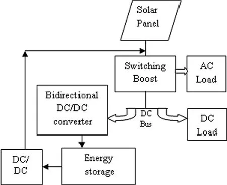
Fig.1 Proposed nanogrid structure
The circuit diagram of the proposed inverter, supplying both DC and AC local loads is shown in Fig.2.The different components in the proposed inverter include: an H bridge inverter (SL1, SL2, SL3and SL4) with LC low-pass filter formed by LLfand CLf, source voltage Vs, a source side diode Dsand load side diode DL, a source side active switch Ss, an inductor Lmand capacitor Cm.The DC output of the inverter can be obtained between the terminals D0and D1, and AC output between terminals A0and A1, as shown in Fig.2.Cmand CLfplay important roles in stabilizing the AC and DC output voltages.The battery storage system is connected across points D0and D1, and the DC/DC converter is connected between the battery storage device and the DC source Vs.The DC to DC converter will be in operation only when radiation descends below a certain level, while the change over from main source to converter can be designed according to the users’ requirement.

Fig.2 Circuit diagram of proposed nanogrid structure
In this work, the energy storage device provides the supply in the absence of the main source.
The main source considered in this work is a solar photovoltaic cell, whose power generation depends on the radiation level and the generated power increases with increase in radiation.As both the AC and DC loads need to be supplied during the day and night, the change over from energy storage device to main source of energy or vice versa depends upon the amount of radiation and power generated by the photovoltaic.
The assumption made here is that the radiation variation curve is trapezoidal.During the start and end of the day the radiation varies, while during day time radiation is considered to be constant.
During the night, no radiation and no source power is available, so change over takes place from the source to the energy storage device.This change over avoids the situation of simultaneous presence of the source power and energy storage device at the input.
4 Steady state analysis
For the complete circuit diagram shown in Fig.2, the operations of the inverter during the day and night are the same except for the difference in the source input.During the day, the solar panel is the source while at night, the source changes to the battery storage.

Fig.3 Operation of inverter in (Dc.Tp) interval

Fig.4 Operation of inverter in ((1 − Dc).Tp) interval
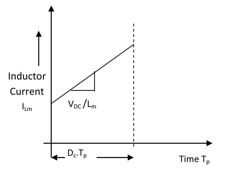
Fig.5 Inductor current ILm during interval Dc.Tp
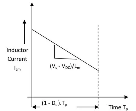
Fig.6 Inductor current ILm during interval (1 − Dc).Tp
Figure 3 shows the operation of the circuit during the shoot through interval with the switch Ssturned on.Assuming the switching period is Tpand the switching duty cycle for switch Ssis Dc, the shoot through interval is Dc·Tp.During this period, VDCis greater than Vsso the diodes Dsand DLbecome reverse biased.The source Vsbecomes inactive and the DC load, inductor Lmand capacitor Cmare in parallel.The capacitor Cmcharges the inductor Lmand supplies power to the DC load.Figure 4 shows the inductor current ILmduring the interval of Dc-Tp, in which ILmincreases.
When the switch Ssis off the circuit operates in the,non-shoot through interval with the duration given as[(1 − Dc).Tp], as shown in Fig.5.In this interval, diodes Dsand DLare active, while the inverter bridge is represented by a current source.The supply voltage Vsand voltage across inductor Lmtogether feed the power to the remaining circuits.The capacitor Cm, DC load and inverter are connected in parallel.In this interval, current through inductor Lmdischarges in three parts: charging current for Cm, current feed to the DC load (IDC) and to the inverter.The inductor current should be maintained in such a way as to have continuous operation of the diodes Dsand DL.Figure 6 shows the inductor current ILmduring the interval (1 − Dc) − Tp.
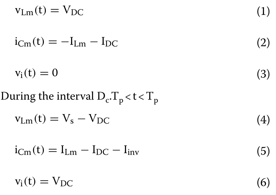
From Figs.3 and 4, the following equations can be obtained.
During the interval 0 < t < Dc.Tp
The bidirectional converter in the circuit can be eliminated by choosing the voltage of the storage device to be same as the inverter input voltage.This will also increase the voltage stability of the DC bus.During the night, as the photovoltaic input source is replaced by the energy storage device, a buck converter is needed to step down the voltage to match the input voltage level.In this condition, only AC load is to be supplied from the input, as the battery supplies the DC load directly.Thus, the source voltage is equal to the step-down battery voltage i.e.

where Vbatis the step down voltage of the energy storage device.
5 Operation during night
The operation of the system during the night is explained in Fig.7.As the RES is inactive during this period, the DC load is supplied by the battery storage system.For supplying the AC load, the DC / DC converter output is connected at Vsterminals.For the change over from main source to converter output it is necessary to take precautions, while the operation of the inverter is the same as previously described.
There are three modes of operation in this condition i.e.:
1.DC load only
2.AC load only
3.Both AC and DC loads
1.DC load only
In this mode of operation, only the DC load is connected to the system.As the main RES is inactive, the load is supplied by the storage system.This represents the simplest operational mode of the circuit.In this paper voltage rating of the DC bus is equal to the battery voltage rating, to avoid the need for a bidirectional converter.The system operation is illustrated in Fig.8.
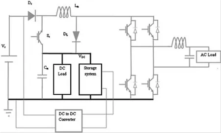
Fig.8 Only DC load during night
2.AC load only
In this mode of operation, only AC load is connected in the circuit and DC load is disabled.As the main source is inactive, battery supplies power at those terminals.In this condition, the complete circuit is active,(except DC load), as shown in Fig.9.According to Fig.9, the voltage VDCat terminals D0–D1is slightly higher than that of the battery voltage.If the AC load in the system is very small, the battery could be charged.To avoid this condition additional battery protection is designed in the system to avoid a possible infinite loop of charging and discharging.With the increase of the load in the system, battery charging will not occur.

Fig.9 Only AC load during night
The H-bridge inverter operates according to the PWM technique while the battery will continue to supply power until reaching the deep discharging protection point.
3.Both AC and DC load
In this mode of operation, both AC and DC loads are present, and Fig.10 shows the operation of the circuit.This is a combination of the above two modes of operation.The DC load in the circuit is directly fed by the storage system while the AC load is supplied through the DC / DC converter and the inverter.
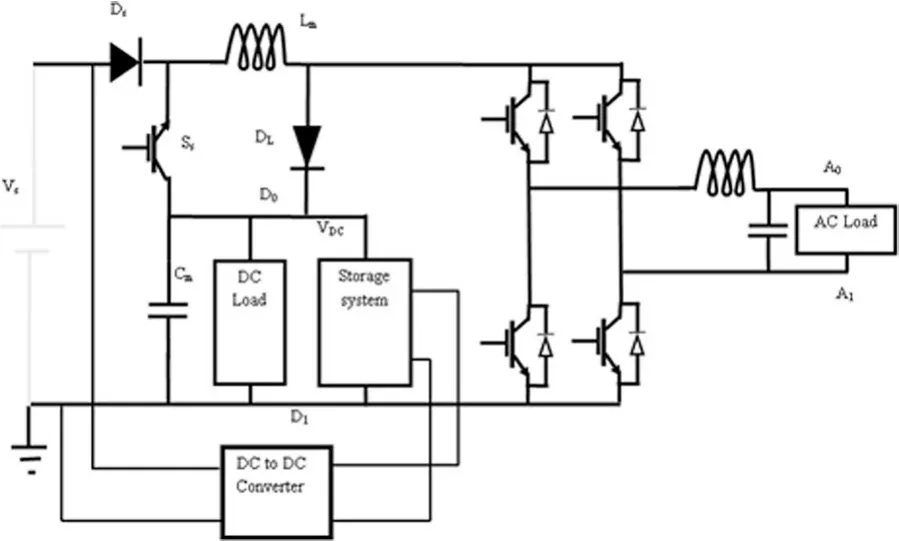
Fig.10 Both AC and DC load during night
6 Results
6.1 Overcharging protection
The overcharging of the battery can lead to permanent damage or life reduction of the battery.The overcharging may also liberate poisonous H2S gas.Figure 11 shows the different periods of the battery charging operation and overcharging protection.
Period o–a: This is the starting of the system.During this period, no power is generated by the solar panel.As the battery has some initial charge (assumed), it starts conducting, as seen in the initial positive current peaks.Generally it is neglected for the calculation(leakage current).
Period a–b: The system is set for the variation in the radiation from zero to its maximum so the ramp is seen in the power in Pin.As the power increases, the battery is charged and its power is shown as negative values in Fig.11.The current also increases from zero to its maximum value (negative) depending upon the generated power from the solar panel.
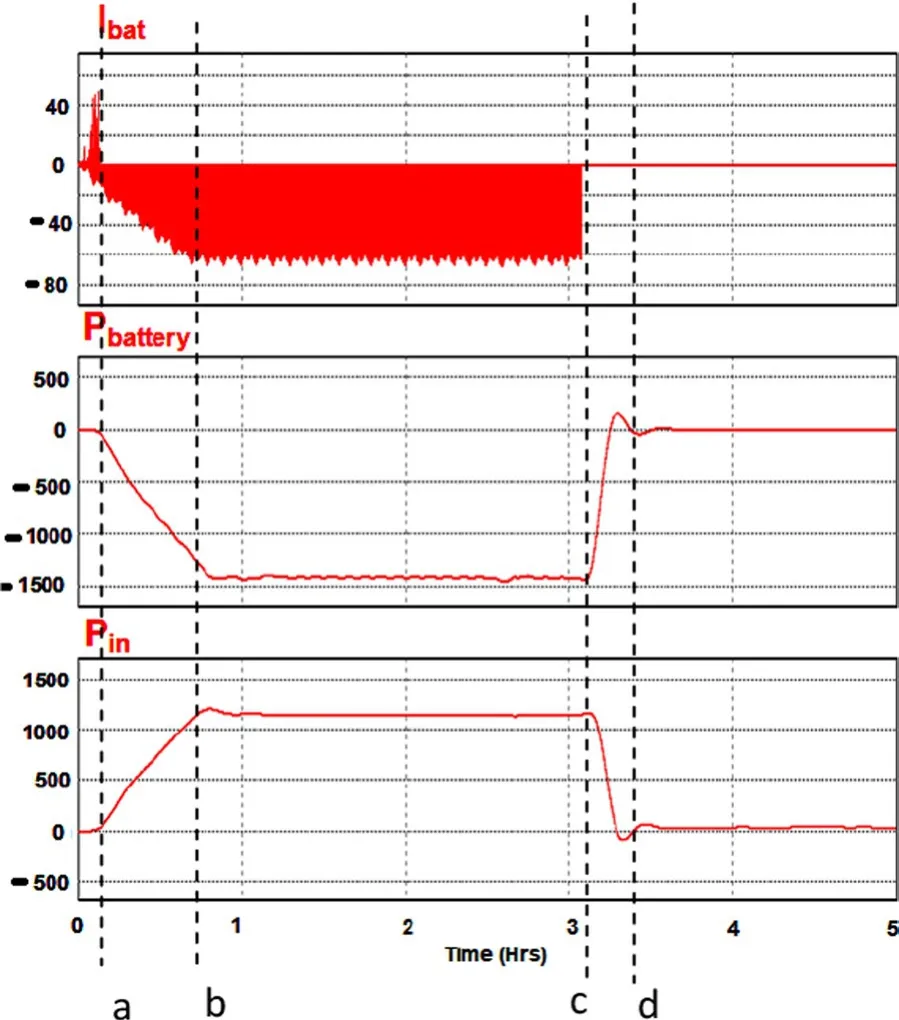
Fig.11 Battery protection system—over charging
Period b–c: Power generation by the solar panel is stable, so the charging current by the battery is also stable during this period.Hence the power taken by the battery in the Pbatcurve is stable as can be seen.
Period c–d: Battery gets fully charged and its protection system for overcharging is activated to disconnect the battery from the supply.Thus the current is rapidly reduced to zero and so is the battery power Pbat.As there is only a very small load in the system, Pinreduces to very low value.
6.2 Deep discharging protection
Similar to the overcharging protection of the battery,deep discharging protection or over discharging protection is also very important.Up to the deep discharging point, e.g., after discharging of 95% of the total battery energy, further discharge of the battery to supply power to the load can lead to a sharp drop in its terminal voltage.
If a battery is discharged beyond a certain limit, it may not be charged again with normal charging.In addition, if deep discharging occurs frequently, the battery could lose its capacity and hence reduce its life time.To avoid this situation, deep discharging protection is provided.
If the load is removed from the battery before the point of deep discharging, the battery terminal voltage can be raised to the normal voltage.However, the voltage recovery of the battery will not be possible if the battery has high self-discharging or is connected to parasitic loads.Surrounding temperature also plays an important role in deep discharging and the cut-off voltage of the battery.
Figure 12 shows the different periods of the battery discharging operation and deep discharging protection.
Period o–a: The load is small and hence an only small current flow through the battery and the power (positive)taken from the battery is also small.
Period a–b: The load increases and hence the power taken from the battery also increases.The current is changed from low to a new high value.
Period b–c: At point “b”, the load again increases so the current and power also increase.At point “c”, deep discharging protection of the battery is activated, and the battery current and power reduce to zero.
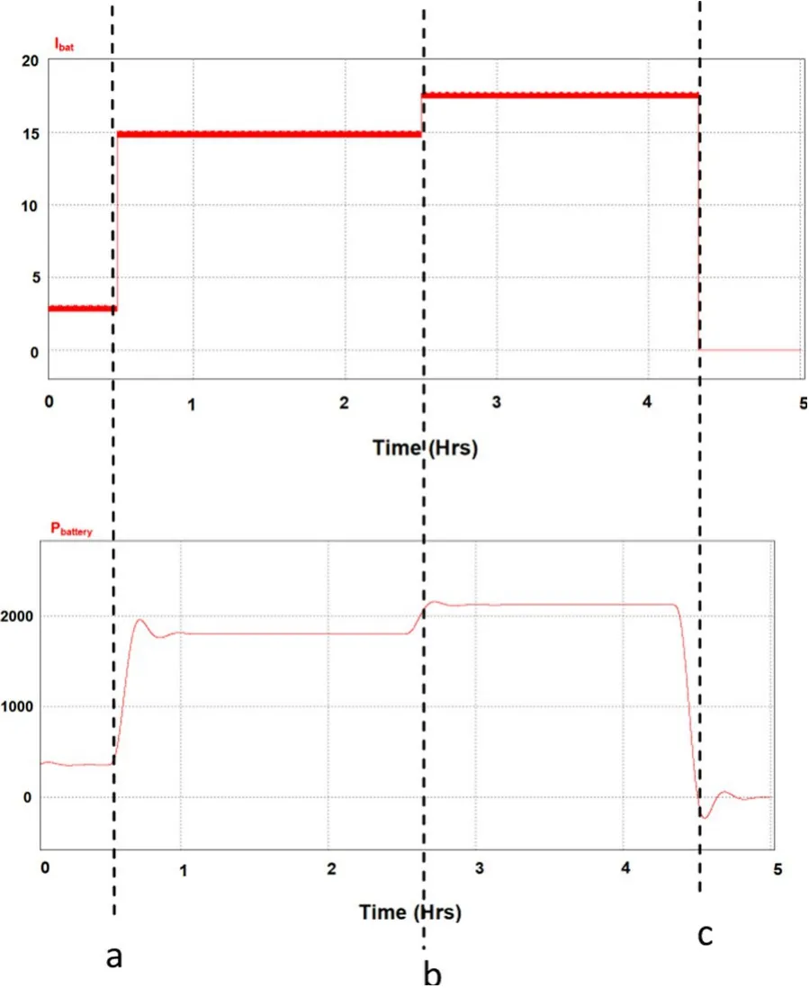
Fig.12 Battery protection system—deep discharging
7 Conclusion
In a hybrid power station both AC and DC power need to be available according to the requirement of the loads.In this paper, a single stage power converter is designed and modelled for both AC and stepped DC output.The designed inverter has many advantages over the traditional two-stage DC to AC converters.
Both the AC and DC bus voltages are regulated to their reference values under steady-state and dynamic load variation conditions of the nanogrid during the day and the night.The simulation results confirm the suitability of the inverter.This, ensures long life of the energy storage system and its control strategy for the hybrid nanogrid system.
It is also shown that the presented system can supply continuous power.The different conditions of the power flow are explained, and the protection of battery overcharging and deep discharging is also shown.The simulation results show that the protection scheme operates satisfactorily.Thus, the suggested converter and control scheme can be effectively used for a nanogrid.
Abbreviations
RES: Renewable energy source; THD: Total harmonic distortion.
Acknowledgements
Not applicable.
Authors’ information
Sachin P.Jolhe received the B.E.degree in electrical engineering from Amaravati University, Amaravati, India, in 2001, and the M.E.degree in electrical engineering from the Government College of Engineering, Karad, India, in 2003.He is currently pursuing the Ph.D.degree in electrical engineering with Government College of Engineering, Chandrapur, India.His research interests include modeling and control of grid-tied inverters, power electronics applications in microgrids/nanogrid, and renewable energy systems.Gunwant A.Dhomane was born in Wardha, India on 1963.He received B.E.degree from Walchand College of Engineering, Sangli, India, in 1986 and M.E.degree from Government College of Engineering, Amravati, India, in 1995 and the Ph.D.degree from Visvesvaraya National Institute of Technology, Nagpur, India, in 2010.He has about 30 years of teaching experience at graduate and post-graduate level.His research interest includes Power Electronics Drives and control,high power factor converters, smart Grid and Renewable sources integration.Minal D.Karalkar received the Bachelor’s degree in Electrical Engineering and Master’s degree in Electrical Power System from Dr.Babasaheb Ambedkar University, (DBATU), Lonere, Raigad, India, in 2001 and Bharati Vidyapeeth,Pune in 2012 respectively.She is currently pursuing her Ph.D.degree in the Department of Electrical Engineering, Government College of Engineering,Amaravati, India.Her research interests include distributed generation and power electronics.power electronics for distributed generation, power quality,and control and protection of microgrid/ nanogrid.
Authors’ contributions
The Protection and Control Scheme for Hybrid Nanogrid is Designed, modelled and analyse in software.The results are presented.All authors read and approved the final manuscript.
Funding
Not applicable.
Availability of data and materials
Not applicable.
Declarations
Competing interests
The authors declare that they have no known competing financial interests or personal relationships that could have appeared to influence the work reported in this paper.
 Protection and Control of Modern Power Systems2021年0期
- Protection and Control of Modern Power Systems的其它文章
- A comprehensive review of DC fault protection methods in HVDC transmission systems
- Application of a simplified Grey Wolf optimization technique for adaptive fuzzy PID controller design for frequency regulation of a distributed power generation system
- A critical review of the integration of renewable energy sources with various technologies
- Operational optimization of a building-level integrated energy system considering additional potential benefits of energy storage
- An integrated multi-energy flow calculation method for electricity-gas-thermal integrated energy systems
- Sliding mode controller design for frequency regulation in an interconnected power system
