基于自适应相关多采样技术的CMOS图像传感器列级单斜ADC设计
高 静,衡佳伟,聂凯明,徐江涛
(1.天津大学微电子学院,天津300072;2.天津市成像与感知微电子技术重点实验室,天津300072)
The readout noise originated from the pixel and the column readout chain is a significant factor to limit the performance of CMOS image sensors(CISs).Such readout noise includes the temporal random noise and the quantization noise during A/D conversion phase.Especially under low illumination,the noise has a considerable effect on signal-to-noise ratio(SNR).Considering the cost and performance,smaller device dimensions become a marked trend of CIS development.Since small size allows for a rise in the number of devices without increasing the chip area[1].However,the noise level is deteriorated as a small pixel source follower(SF)contributes worse temporal random noise in the readout circuits.Therefore,it is necessary to enhance SNR by mitigating the noise level.In general,it is an effective approach to reducing noise by using low-noise readout circuitry.The column-parallel single-slope(SS)ADC has been widely applied in CIS.The reason is that it provides relatively low noise with simple circuit topology,small area,and low power consumption.
Recently multiple-slope architecture[2-3],pre-amplifier with gain-adaptive[4-6],and correlated multiple sampling(CMS)technique[7-11]have been presented to reduce the noise.The CMS technique employed in SS ADC is effective for suppressing the random noise originating from the in-pixel SF and the readout circuit.However,the total conversion time increases linearly with the number of sampling times(M),which slows down the readout speed.This problem is solved by using the two-step ADC architecture[12-13]or two-column ADCs for the parallel multi-sampling[14].Nevertheless,the larger power consumption and circuit area are serious problems.Additionally,a random noise reduction technique has been reported while keeping the A/D conversion time[8].The basic concept of the technique is to utilize a triangle waveform reference,which controls the number of sampling.However,owing to the average operation,the integer divider occupies a large area.Furthermore,a pseudo-multiple sampling technique has been achieved as well[10-11],which alters the resolution of SS ADC according to the number of samplings.It is an effective way to keep the readout speed,along with noise reduction by dividing a higher resolution A/D conversion into a few lower resolution conversions.However,the quantization noise limits the readout noise suppression.
In this paper,a column-level SS ADC with an adaptive correlated multiple sampling(ACMS)technique is introduced to selectively reduce the readout noise.The basic concept of the proposed technique is that the range and gain of the ramp signal adaptively alter according to the output swing of pixels.For the small-swing signal,a ramp with small-range and highgain is applied for the CMS operation.In contrast,for the large-swing signal,a ramp with large-range and lowgain is enough.The reason is that SNR is dependent on the photon shot noise at high light intensity,which cannot be reduced by multi-sampling operation in a single frame[7].Therefore,the low readout noise is needed at low light while at high light it could be relaxed slightly without too much penalty on SNR.The proposed ACMS method reduces the random noise and the quantization noise in low light conditions.Moreover,the method solves the low frame rate problem of conventional CMS.A simple digital circuit with the signal swing detection function is designed as well.In this circuit,the suitable ramp signal is selected by means of the comparator output.
1 Conventional CMS technique
The A/D conversion of SS ADC is accomplished by lots of comparisons between the analog input voltage and a ramp voltage.Although the method is simple,it requires 2nclock periods for eachn-bit conversion.The scenario becomes worse when the multiple sampling operation is used for the A/D conversion.The conversion time is linearly proportional to the sampling times,which will significantly affect readout speed.Additionally,as the sampling time increases,the noise suppression capability of the CMS is limited by the low-frequency noise,i.e.,1/fand random telegraph signal(RTS)noise from the in-pixel SF[15].For further noise reduction,it is necessary to reduce the A/D conversion time of the multiple sampling operation.
For the pixel output signal,in the initial phase,the pixel cell is reset and the reset level is output.Then,the signal level of the pixel is output after the exposure.The signal level is gradually decreased as the light intensity is increased.Therefore,the swing of the pixel output signal is proportional to the light intensity.Fig.1 shows the ramp and pixel output waveform of the A/D conversion with 3-times sampling operation.At low-light illumination,most of the full-range ramp is not valid because the output swing of the pixel is small.Therefore,the effective A/D conversion time is short.Accordingly,an ACMS technique is presented to overcome the drawbacks of the conventional CMS technique.
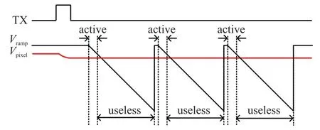
Fig.1 Conventional CMS readout scheme with small output swing
2 Proposed ACMS technique
There are two main noise sources in SS ADC,namely,the input-referred random noise and the quantization noise of ADC.The main temporal random noise is contributed by the noise of in-pixel SF,pre-amplifier,and ADC.After digitization,the output of ADC will have an additional quantization noise.It is expressed as:

whereVqunis the quantization noise depending on the resolutionn,VLSBis the quantization step size,andV Ris the input range of SS ADC.The quantization error is approximated as“white noise”.
The relationship between incident light illumination and various noise sources is plotted on a graph,as shown in Fig 2(a).Most of the random noise is not influenced by light intensity.These noise sources form the constant random noise,including thermal,1/f,and RTS noise.The readout noise consists of constant random noise and quantization noise,which is a key factor to limit SNR under low illumination.In addition to readout noise,photon shot noise is present in CIS.During the exposure time,the number of photons striking the sensor is random,which results in the shot noise.The relation between the number of photoelectrons(Nsig)in the signal and its associated noiseNphs(both expressed by the number of electrons)is given by:

Since the shot noiseNphsdepends on theNsig.Thus,under high illumination,SNR is limited by the shot noise.The readout noise does not have to be as low as it should be for the small-swing signal.
Accordingly,an ACMS technique is proposed to compensate for SNR while keeping the frame rate.Relying on the light intensity,the suitable ramp voltage is automatically selected.For high-light pixels with the large output signal,a full-range and low-gain ramp is enough.Conversely,for the small-swing signal,the ACMS technique utilizes a small-range and high-gain ramp multiple times.In this way,the constant random noise is reduced by a large number of samplings and the quantization error would be improved with the highresolution.Therefore,SNR is enhanced by the proposed ACMS technique at low-light levels,as shown in Fig.2
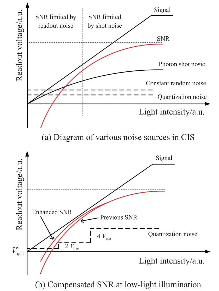
Fig.2 Conceptual plot of the relation between light illumination and noise
(b).
If the constant random noise is low enough by increasing the sampling number,the quantization noise becomes the limiting factor of the SNR at low light.Therefore,instead of a linear ramp,a piece-wise-linear ramp signal is adopted.For simplicity,the piece-wise-linear ramp is supposed to be a binary increasing gain.As shown in Fig.2(b),the quantization noise increases fromVqunto 2Vqun,then to 4Vqun,etc.
The resolution of the piece-wise-linear ramp should be matched to the random noise.Therefore,it is essential to compute the pixel output levels at which the resolution and the number of sampling times need to be increased.A simple quality factorκis defined as follows:

whereVphsis the shot noise voltage.The output thermal noise powerand 1/fnoise powerafter the CMS process are given by Refs.[16-17]

whereS ntis the power spectrum density of the thermal noise,T0is the sampling period,k fis the flicker noise coefficient,andCi nandC f bare the input capacitor and the feedback capacitor of the pre-amplifier,respectively.
The condition of the pixel output signal level is computed by combining equations(1)through(5),which yields the following expression:

whereqis the elementary charge,GSFis the SF gain,Gamprepresents the voltage gain of the pre-amplifier,CFDis the capacitor of the floating diffusion(FD)node,andVrstandVsigare the reset level and signal level of the pixel output,respectively.According to equation(6),the optimal division of the signal level is obtained.
SNR is the ratio between the signal and the total noise at a given input level.From Fig.2(a),it is clear that SNR should have different expressions under different illumination conditions:

whereNreadis the readout noise.According to formula(7),the factorκis set to 0.4 and 0.04 under low and high light conditions,respectively.It is a conservative design to ensure that both the quantization noise and the random noise maintain a sufficiently low noise level.Considering the range of pixel output and ADC input,the default gain of the pre-amplifier is 2×,where CISs offer the maximum dynamic range.Conservatively,the initial resolution is 12-bit and the gain ratio of adjacent ramps is set to 6 dB.To sufficiently reduce noise by a large number of samplings at low-light illumination,M=2 is employed for the maximum ramp signal(ramp1).A summary of such a piecewise-linear ramp is given in Table 1.Each ramp covers a part of the signal swing.
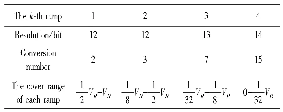
Table 1 Summary of the piece-wise-linear ramp scheme
As can be seen in Table 1,the SS ADC with ACMS technique provides 12 to 14 bits variable-resolution in different ADC input ranges.The darkest pixel output signal is converted 15-times whereas the brightest one is done twice.Unlike the default ramp signal(ramp1),other ramps require to be reset after switching the ramp signal according to each comparator output.Thus,reset operation needs to be subtracted from the number of signal conversion times.In addition,the compensation among sampling number,resolution,and the ramp range forbids the counter overflow.
Another advantage of the piece-wise-linear ramp is that the conversion time is not increased.In the proposed ACMS technique,TACMS,the total A/D conversion time with thek-th ramp,is given by:

wheren0is the initial resolution of the SS ADC andTclkis the period of the counter clock.TCMS,the total A/D conversion time of conventional CMS,is given by:

Fig.3 shows the total A/D conversion time histogram under different sampling number.n0=12 bit andTclk=5 ns in this paper.For proposed ACMS,the total conversion time is kept 40.96μs.For 15-times multiple sampling,the ACMS technique achieves a 7.5×reduction in A/D conversion time compared with the conventional CMS.

Fig.3 A/D conversion time with proposed ACMS and conventional CMS
3 Circuit design and operation principles
3.1 Column-parallel SS ADC
The column-parallel SS ADC is shown in Fig.4(a)along with the typical 4T pixel structure and preamplifier.The programmable gain amplifier(PGA)is an inverting voltage amplifier with 1×-8×variable analog gains(Gamp).The variableGampis dictated by the capacitance ratio ofC i n/C f b.The SS ADC with ACMS function consists of a multiple-ramp generator,a comparator,an up-counter,two latches,and a ramp selector.
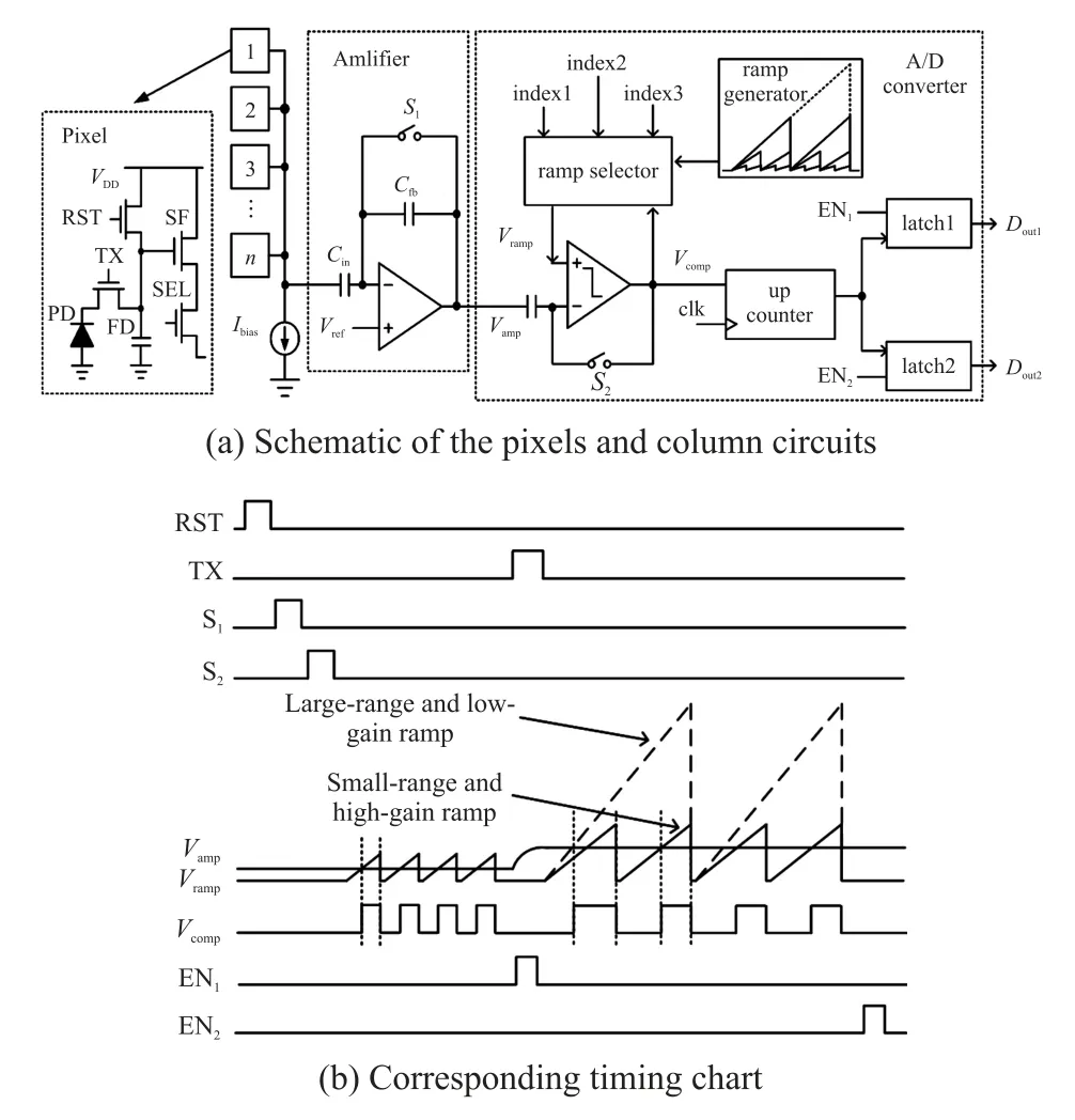
Fig.4 Column-parallel SS ADC design and operation principles
Fig.4(b)shows the timing chart of the pixel devices and column readout circuits.Firstly,the photodiode(PD)and FD node of pixel are reset.The pre-amplifier and comparator are reset sequentially.The switch RST,S1,andS2are closed sequentially to isolate both the offset voltage and reset noise of every stage in a next capacitor[18-19].The noise is cancelled by the ACMS method later on.The up-counter is also reset at the same time.Then the amplified reset voltage is compared with the ramp signal generated by the multiple-ramp generator.In the case ofN-times amplified reset voltage sampling,the up-counter begins counting up synchronously when the comparator output(Vcomp)is“H”during the conversion phase.Finally,the reset voltage sampling data in the up-counter is stored in latch1 by enabling EN1.The latch1 output(Dout1)corresponds toN-times sampling of the amplified reset level and the offset voltage,which is expressed as:

whereDrst,Nis theN-times sampled data of amplified reset voltage andDoffset,Nis the included offset voltage afterN-times multiple sampling.
After the TX is closed and the photo charge from the PD is transferred to the FD node,TheVampascends to the amplified signal level accordingly.The conversion of signal level is divided into two phases,namely,a ramp selection phase and an A/D conversion phase.To save time,the first phase is combined with the second conversion phase.During the selection phase,the SS ADC compares signal voltage with ramp1 by default.Based on the results of the ramp selector(the detailed method is described in Section 3.2),each comparator is connected to the most appropriate ramp among ramp1,ramp2,ramp3,and ramp4 when the comparator flips.After selecting the ramp,the operation phase moves to the second and the subsequent multiple-sampling function is performed.Similarly,the signal voltage sampling data in the up-counter is stored in latch2 by enabling EN2.Dout2is expressed as follows:

whereDsig,Mis theM-times sampled data of amplified signal voltage andDoffset,Mis the included offset voltage after multiple sampling.The final data processing is achieved byDout1,Dout2,and the output of the ramp selector.The final output(Dout)for each pixel is expressed as follows:

Thus,the offset voltage is eliminated by digital correlated double sampling(D-CDS).
The proposed ACMS technique is realized using a classical SS ADC architecture by changing the ramp generator.In this paper,four ramps are required.Therefore,the proposed technique increases area and power consumption due to the multiple-ramp generator.For a large-array CIS,the increase of area and power has a small impact.Since the multiple-ramp generator is shared by all column ADCs.The four ramps have different gains and ranges.However,the gain and range of the ramps are unchanged during the second conversion phase,which decreases the possibility of SS ADC nonlinearity and instability.
3.2 Ramp selector
The core idea of the ACMS technique is to abate readout noise in such a way that the suitable ramp signal is automatically chosen by the comparator output.Relying on the ACMS technique,SNR is compensated,especially at dark-light illumination.Thus,it is necessary to detect the amplified signal swing before A/D conversion.
The designed ramp selector with its timing diagram is depicted in Fig.5.VampandVcompare the pre-amplifier and comparator output,respectively.Three index signals(index1,index2,and index3)are used to divide signal swing.Initially,the maximum ramp signal(ramp1)is connected to the comparator by resetting all DFFs to“L”.Once the comparator output flips from“L”to“H”,DFFs are used to lock the level of the three index signals.For example,in the case of Fig.5,a logic“011”is latched by the DFFs and stored in a data memory.Next,the logic value is fed back to a 3-to-8 decoder,which connects the suitable ramp to each comparator.The corresponding relationship between the output of the three DFFs(Q1Q2Q3)and the selected ramp is given in Table 2.
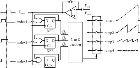
Fig.5 Designed ramp selector with its timing diagram

Table 2 Relationship between Q1 Q2 Q3 and selected ramp
The ramp selector only requires some extra switches and digital circuits in every column.Therefore,the selector only leads to the slight increment of the area and power consumption.
3.3 Multiple-ramp generator
The proposed SS ADC requires four ramp waveforms instead of only one.Therefore,it is the most critical that the multiple ramps are well-matched.Since capacitors match better than resistors,the multiple-ramp generator is implemented by switch-capacitor(SC)circuits in this paper.There are many different coding architectures,such as binary-weighted,thermometer coded,and segmented DAC.Generally,to reduce the area and power,the DAC based on binary-weighted SC array with an attenuation capacitor is employed[20-21].However,the extra parasitic capacitor would affect the linearity and reliability of the DAC,particularly for the parasitic capacitor of the attenuation capacitor.In addition,the weight of each unit capacitor is different,which causes larger cross-talk and glitches when the state of the switch is changed.Therefore,the thermometer coded SC array is adopted.During each time,there is only onebit change,which is capable of effectively reducing the jitter and unreliability of the ramps[22].Moreover,the differential nonlinearity(DNL)of the ramp voltage is smaller,if the generator does not use the attenuation capacitor.Fig.6 shows a simplified circuit diagram of the proposed ramp generator.

Fig.6 Simplified circuit diagram of the proposed ramp generator
During the reset phase of the ramp generator,the switchSrstis closed.The bottom plates of all capacitors are also connected to the reference voltageVreflvia switchesb i(i=0,1,2,…,2n-1).Then theSrstgets open and the bottom plates of all capacitors are sequentially connected toVrefh.The output voltage of the DAC(VDAC)is given as:

whereaandbare the number of capacitors connected to theVrefland theVrefh,respectively.Anda+b=2n-1.
According to equation(13)and considering the parasitic capacitorC P,VDACis given by:

The parasitic capacitor does not cause the nonlinearity of the ramp signal.However,whena=0 andb=2n-1,the above equation is simplified as:

At this time,VDACis not equal toVrefh,which would reduce the output range of the DAC.This effect is reduced by increasing theVrefh.Thus,the reference voltageVreflandVrefhare generated by a programmable voltage generator(PVG).The PVG is implemented by a set of serial resistors.Every step voltage in the resistor ladder isIbg×Rload,whereIbgis generated by the bandgap voltage,Rloadis the unit resistors.TheVreflandVrefhare increased or decreased by the step voltage.
Another advantage of the programmable voltage is that it could calibrate the offset voltage among multiple ramps.The offset voltage includes input offset voltage of the multiple-ramp generator,unstable reference voltage,and the offset of the output buffer.The offsets cause a vertical shift of the four ramps(the shift of ramp3 and ramp4 are not plotted),as shown in Fig.7(a).The residual error is converted to an incorrect digital code,resulting in a dead band.This error correction scheme is shown in Fig.7(b)with the ramp2 example.The range of the four ramps is programmable via digital codes,which could cover the residual errors.The offset voltage is removed by selecting an appropriate reference voltage.Moreover,the dead bands are avoided by creating some overlap between the four ramps.

Fig.7 Ramp signal plots
Because of the thermometer coded,the mismatch of the capacitors has little effect on the linearity of the four ramps.However,owing to the process mismatch,the gain error causes performance degradation at the threshold voltage between the four ramps.
During the selection phase,the ramp selector switches the ramp voltage from ramp1 to the most appropriate ramp.Therefore,the output digital codes at the threshold voltage between the four ramps are expressed as:
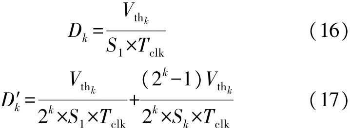
whereVthkis the threshold voltage between ramp1 and rampk(k=2,3,4),S1is the slope of ramp1,Skis the slope of rampk,Tclkis the period of the counter clock,andDkandD′kare the minimum voltage of ramp1 and the maximum voltage of rampk(both expressed by the output digital codes)at the threshold voltageVthk,respectively.The error is calculated as:

From equation(18),the sampling number(M=2k)also affects the error.The problem is easily solved by resetting the up-counter after switching the ramp signal.At this time,equations(17)and(18)are rewritten as follows:
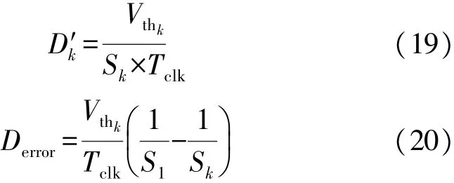
From equation(20),the sampling number(M=2k-1)does not affect the error.Furthermore,to minimize the error,calibration technique is needed to calibrate the slope mismatch at the threshold voltage.A gain ratioβkof the four ramps is defined as:

The calibration technique is shown in Fig.8.Three preset voltagesV1,V2,andV3are offered from a DAC.In the beginning,the preset voltagesV1is converted by both ramp1 and rampk to obtainD1,LandDk,L,where the SS ADC is forced to connect to either ramp1 or rampk.Then the preset voltagesV2andV3are converted sequentially by rampk and ramp1 to obtainDk,HandD1,H.Finally,the gain ratioβkis calculated as:

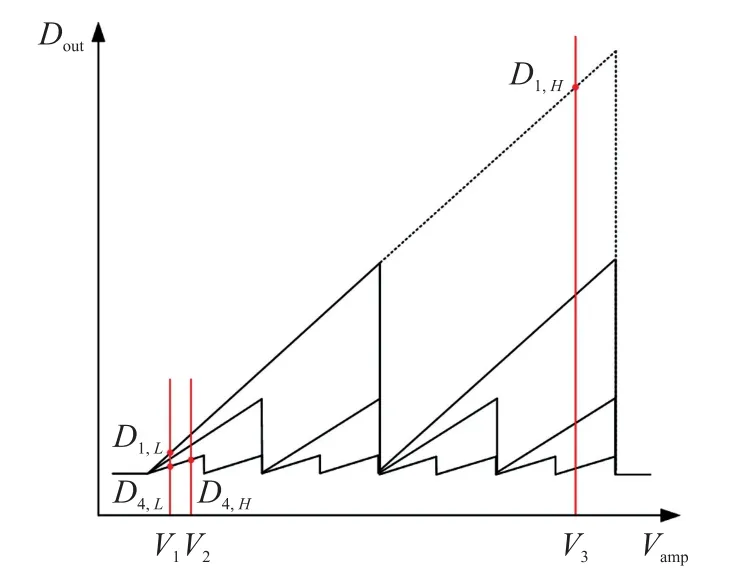
Fig.8 Calibration technique of the gain error
The digital output is calibrated byβkat the connecting points between the four ramps.Note that three preset voltages are not close to the connecting points.Since the better linearity and reliability in the middle of the four ramps.Combined with the description in Section 3,Fig.9 illustrates the CIS readout and calibration flow with the ACMS technique.

Fig.9 CIS readout and calibration flow with the ACMS technique
4 Simulation results
The presented ACMS technique based on SS ADC is designed and simulated in a standard 0.11μm CMOS process.The supply voltage is 3.3 V for analog circuitry and 1.5 V for digital.A complete A/D conversion period from PGA to the SS ADC is set to 64μs,and it does not increase with the sampling number and resolution.The ADC provides 12 to 14 bits variable-resolution in different input ranges.The power consumption of each column is 125μW,which includes the consumption of the SS ADC(90μW)and the PGA(35μW).Moreover,the layout of column-parallel PGA and ADC is illustrated in Fig.10.The single-column PGA and ADC occupy the area of 6μm×750μm and 6μm×880μm,respectively.

Fig.10 Layout of designed PGA and SS ADC
The linearity and reliability of the SS ADC is determined by the performance of the multiple-ramp generator.Fig.11 shows the simulation results of the generator output signal.The ramp signal waveforms are relatively smooth and glitch-free.After the calibration of the offset voltage,the simulated DNL and integral nonlinearity(INL)of the ramp signals are shown in Fig.12.The DNL and INL are+0.001 36/-0.001 86 LSB and+1.609/-1.677 LSB,respectively.Furthermore,the noise of the entire multiple-ramp generator is 31.2μVrms.Thus,the multiple-ramp generator meets the accuracy and reliability demands without serious nonlinear problems.
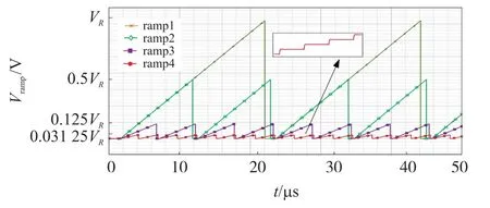
Fig.11 Simulation results of the generator output signal
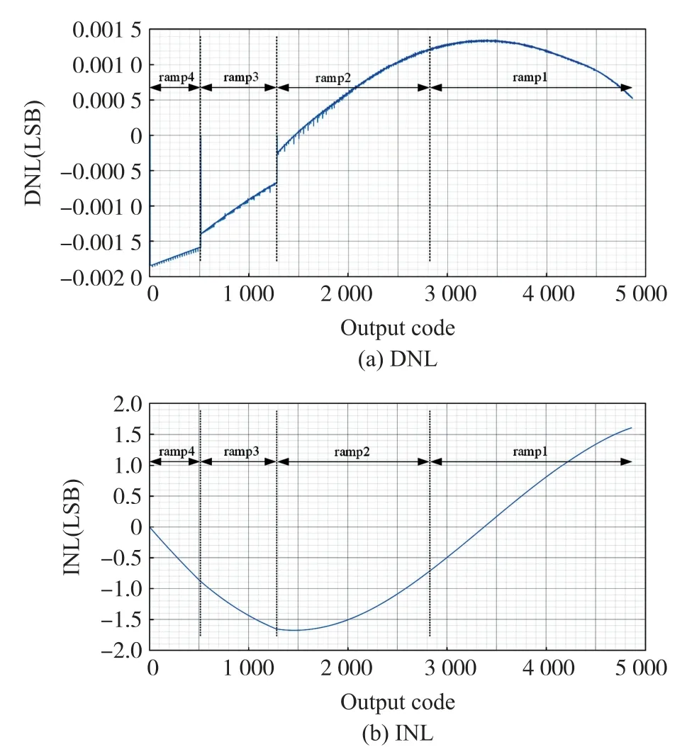
Fig.12 Performance of DNL and INL
The simulated input-referred random noise under different PGA gain modes is shown in Fig.13.The input range of the SS ADC is divided into four intervals.As the input voltage decreases,the input-referred random noise is reduced from 200μVrmsto 90μVrmsatGamp=2.The temporal random noise reduction of the proposed ACMS technique is about 55% in low-light conditions.The random noise decreased with the increase of sampling number and PGA gain until it is finally down to 59μVrmsatM=15 andGamp=8.Another observation concluded from Fig.13 is that the noise reduction effect of the ACMS technique declines slightly at higher gain settings.
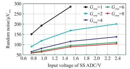
Fig.13 Simulated input-referred random noise under different PGA gain
The input-referred readout noise after the proposed ACMS process is shown in Fig.14.As the input voltage decreases,the readout noise is reduced from 211μVrmsto 92μVrmsatGamp=2.The noise reduction corresponds to 7.21 dB SNR improvement at low-light-level illumination.Compared with the random noise in Fig.13,the readout noise is only slightly increased in low light conditions.The conventional CMS is applied(Gamp=1,M=3,and 12-bit resolution)for comparison,the simulated readout noise is about 300μVrms.However,by applying ACMS technique(Gamp= 1,M= 3,and 12-bit resolution),312 μVrmsreadout noise is obtained.Equation(4)means that the ACMS technique with reducedT0increases the thermal noise.However,the 1/fnoise decreases with theT0decreases as equation(5)suggests.Therefore,in this paper,the dominant noise contributor is the thermal noise,instead of the 1/fnoise from the pixel SF.For the same M,though the noise performance of ACMS is slightly worse than the CMS,the A/D conversion time is effectively reduced.The simulation results confirm that the novel presented ACMS scheme achieves a good noise reduction effect while without any increase of total A/D conversion time.

Fig.14 Simulated input-referred readout noise after the ACMS process
Combining equation(2),the shot noise of the pixel is added by generating the random number using the Poisson distribution.Fig.15 shows SNR curves with proposed ACMS and conventional CMS(forM=2)technique atGamp=2.For large signals,the points of both curves are completely coincided.The reason is that the large signal is the shot noise dominated which cannot be reduced by the ACMS technique.For small signals,SNR is enhanced by the ACMS technique.Therefore,the proposed ACMS reduces the readout noise at low light.

Fig.15 The relation between SNR and signal(expressed by the number of electrons)with proposed ACMS and conventional CMS technique
Table 3 lists a noise performance summary and gives a comparison of this work with the prior arts.Compared with Refs.[8,12-13,23],this work achieves the state-of-the-art performance in input-referred random noise.The figure of merit(FoM)in Table 3 is defined as:

Table 3 Performance summary and comparison

wherevnis the input-referred random noise andTADCis the total A/D conversion time for each pixel output.This paper achieves a good FoM of 3.77 nVrms·s,which means the simultaneous capability of maintaining both low noise and high speed.
5 Conclusion
In this paper,an ACMS technique is presented to selectively suppress random noise and quantization noise according to the signal swing.The SS ADC architecture incorporates four ramps with different gains and durations.Each ramp covers a part of the input range of the ADC.Moreover,the calibration methods of offset voltage and gain error improve the linearity of the ramp signals.The simulated DNL and INL of the ramp signals are+0.001 36/-0.001 86 LSB and+1.609/-1.677 LSB,respectively.The proposed column-parallel SS ADC achieves 59μVrmsreadout noise atM=15 andGamp=8.The improvement of SNR is 7.21 dB atGamp=2.Additionally,The FoM of the implemented ADC realizes 3.77 nVrms·s while keeping the A/D conversion time.The simulation results show that the suggested ACMS technique successfully mitigates readout noise and enhances SNR at dark-light illumination.
Acknowledgments
This work was supported by the Tianjin Key Laboratory of Imaging and Sensing Microelectronic Technology.

