Bias-controlled spin memory and spin injector scheme in the tunneling junction with a single-molecule magnet∗
Zheng-Zhong Zhang(张正中) and Hao Liu(刘昊)
1Faculty of Mathematics and Physics,Huaiyin Institute of Technology,Huaian 223003,China
2Nano Science and Technology Institute,University of Science and Technology of China,Suzhou 215123,China
Keywords: single-molecule magnet,spin-transfer torque,spin-dependent electron tunneling
1. Introduction
Exploring the spin degree of freedom in quantum systems, such as single-molecule magnets (SMMs) and singleatom magnets, is an emerging field of promising applications, from nano-spintronics[1]to quantum information processing.[2]Conventionally, the smallest cell of the magnetic memory consists of 2–12 atoms.[3–5]Very recently, a single holmium atom on the thin film of the magnesium oxide(MgO)is demonstrated as the first example of a stable singleatom magnet.[6]The long relaxation time of the magnetic bit gives rise to the remanent magnetization, causing the limited size of the magnetic bit. Moreover, the experimental work in Ref. [7] shows that the nuclear spin of holmium atom can be reading and writing by a series of electric pulses with the help of spin-polarized scanning tunneling microscope(SP-STM)[8]and single-atom electron spin resonance (ESR) effect on an adjacent iron atom. The observed long lifetime (tens of seconds) and relaxation characteristics of the nuclear spin at the single-atom scale open the way to a completely new world of devices by which quantum logic may be implemented.
Owing to the recent development of material science and technology, there is increasing interest in the investigation of SMM[9]as the candidate for novel electronic devices,[10–12]such as random-accessing memories and spin injectors. Their properties depend on the combination of a large molecular spin and an easy axis magnetic anisotropy,[13,14]which results in a double-well energy potential resisting to the reversal of the magnetization. Controlling these molecules on different surfaces has attracted considerable attention as a prerequisite to single-molecule addressing.[15]In such studies, it was demonstrated that magnetic bistability persists and can be enhanced on some surfaces.[16]Especially efficiency of boosting the memory effect of both molecules and individual atoms can be achieved by depositing them on the thin insulating layer(e.g., MgO) rather than directly on the metal surface.[17,18]Despite these remarkable results, how to electrically control the magnetic bistability of SMM between electrodes remains open.This is in part due to the limited experimental techniques that are sensitive enough to detect the magnetic properties of SMM.
In this work, we propose a novel type of spin filter, by a single magnetic atom coupled to an SP-STM or fabricating the junction with an SMM sandwiched between the normal metal and ferromagnetic (FM) lead. It is predicted that the spin direction of SMM can be readily read out and written by electrical bias pulse applied across the junction,and the highly spin-polarized current can be generated and controlled by this structure. Similar to the experimental work in Ref. [4], the manipulation of SMM’s spin states needs a two-step scheme.First, a relative larger bias pulse is applied to obtain enough large spin-polarized currents to control a spin orientation of the SMM.The spin direction of SMM can be parallel or antiparallel to the magnetization of the FM lead,depending on the direction of the bias pulse.And the measurement process is using a relatively low bias pulse to detect the magneto-resistance or spin-polarization coefficient of tunneling current.
2. Model and Hamiltonian
The system we consider here consists of a single magnetic atom coupled to an SP-STM or sandwiching the junction with an SMM between two leads of normal and ferromagnetic metals as shown in Figs.1(a)and 1(b), respectively. The Hamiltonian for both systems can be written as[19,20]


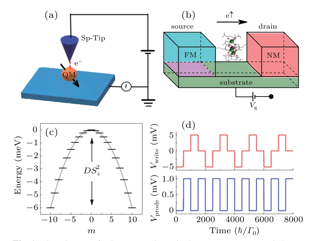
Fig.1. The schemes of spin memory by a single-atom magnets coupled to an SP-STM tip and an SMM sandwich between the FM and NM leads are shown in panels(a)and(b),respectively. (c)Energy spectrum of the molecule with a tunneling barrier DS2z ≈60 K for Mn12−ac.(d)The time varying bias pulses of Vwrite (red)and Vprobe (blue)for“writing”and“reading”processes.
The Hamiltonian of the individual SMM is described by the first five terms in Eq. (1). By definingST=s+S, the eigenvaluemofSzTis a good quantum number due to commutation relation[SzT,H]=0. In the following,|n,m〉representsnelectrons occupying the SMM with the total spin asm. The eigen-energies can be obtained as[21]

In order to read out the magnetization of the SMM by a small bias voltage pulse,we need a magnet molecule with relative large anisotropy. In this paper,we use SMM of Mn12−acwith parameters asD=0.06 meV,S=10,J=0.2 meV,andU= 25 meV.[22,23]This SMM has two degenerate ground states ofSz=±10 and a relative large tunneling barrierDS2z ≈
60 K. Additionally, we assumed the molecule is weekly coupled between two electrodes, so that the transport process is dominated by the sequential tunneling through the SMM energy level, while the cotunneling and direct tunneling can be neglected safely at low temperature.For the weak coupling between the SMM and two leads,the master equation approach is valid for our analysis. The SMM’s magnetization can be defined asMSMM=∑i miPi, and the current of spinσflowing through the SMM can be written asIσ=(ILσ −IRσ)/2,whereILσ(IRσ)stands for the spin current flowing from the left(right)lead to the SMM as

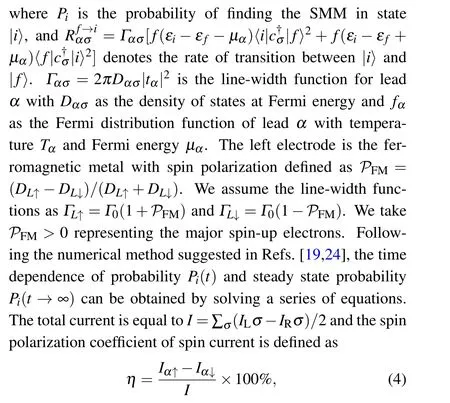
by which the totally-polarized spin current has the coefficient asη=±100%.
3. Result and discussion
First, we demonstrate how the voltage pulse controls the magneto-resistance switch and spin-polarization in a FM/SMM/NM junction. At the low temperature, the SMM must be in one of the two bistable ground statesMSMM=±S.For the sake of definition, we setMSMM= +Sparallel to the magnetic polarization of the left FM lead. As shown in Fig.1(d),an electric pulseVwriteof the amplitude±5 mV is applied to the device,which changes its sign at every 1000/Γ0(∼=20 ns forΓ0=8 GHz[24]) and drive the SMM’s polarization to±Speriodically as shown in Fig.2(d). It is noteworthy that the pulse signal only lasts 500/Γ0(∼=10 ns)every time it reaches±5 mV, and then returns to zero quickly. During the time ofVwrite=0,another series of the pulseVprobedenoted by the blue line in Fig.1(d)is applied to read out the SMM’s magnetization. The total voltage pulseV=Vwrite+Vprobeis shown in Fig.2(a)and the magnetization response of the SMM to the applied pulse is shown in Fig. 2(d). Obviously, the magnetization of the SMM turns to+Sdirection under the“−5 mV”pulse,while the“+5 mV”pulse will reverse the magnetization to−S. As shown in Figs. 2(b) and 2(c), the “+5 mV” pulse will drive the spin-polarization coefficientηprobefrom 100%to−100%,indicating that only spin-down electron can tunnel from the FM lead to the NM lead. A high magneto-resistance is obtained as a result of the anti-parallel magnetic configuration between FM and SMM. Then, after the “−5 mV” pulse is applied, the electron current driven byVproberises quickly and polarization coefficient is increased to +100%, which means only spin-up electron can tunnel through the junction and the low magneto-resistance is obtained. In addition, we show the differentPFMof the FM lead in Fig. 2. Although the current signalIprobewill be suppressed or enlarged by the FM lead’s magnetizationPFM,the polarization coefficients of the spin current in both spin directions are robustly fixed atηprobe=±100%. As a result, the two bistable ground statesMSMM=±Scan be read out byVprobewith the different spinpolarization coefficients and the magneto-resistances.
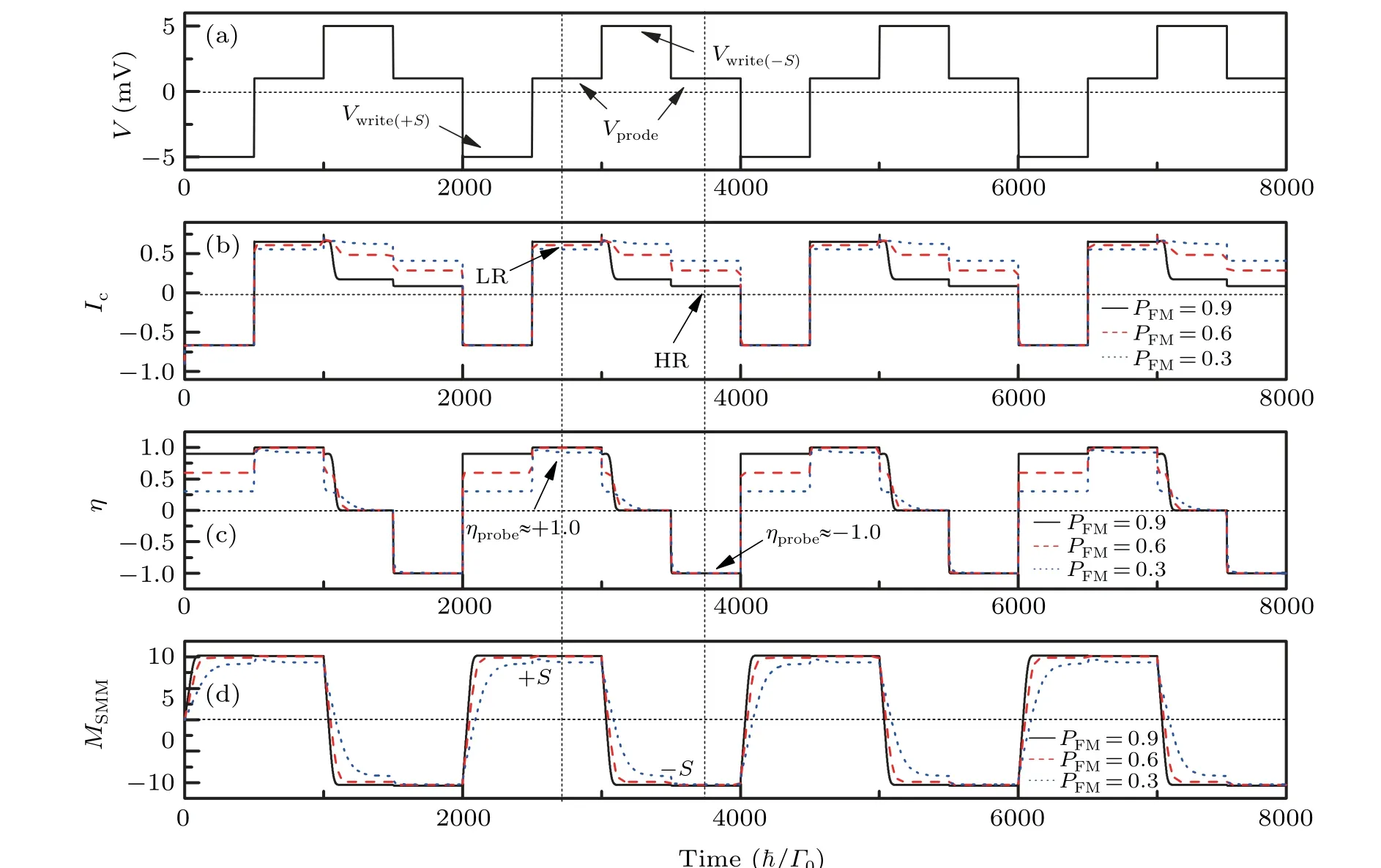
Fig.2. (a)The voltage pulse of V =Vwrite+Vprobe. (b)The tunneling currents(scaled by eΓ0/)for different polarizations of FM leads PFM. (c)The spin-polarization coefficient η. (d)The polarization of SMM MSMM. The initial state is P|0,±S〉=0.5 with ε0=0.5 meV and the temperature T =0.5 K.
In order to clarify the underlying mechanism,we plot the probabilities of molecular states forPFM=0.95. In Fig. 3,the probabilities of the states except|0,±S〉,|1,S+1/2〉,and|1,−S−1/2〉are almost vanishing. In Fig. 3(a), it is shown that before “−5 mV” pulse is applied,P|1,−S−1/2〉+P|0,−S〉is equal to 1, which means the SMM’s spin is fixed at−Sdirection. AfterVwrite=−5 mV is applied,P|1,−S−1/2〉andP|0,−S〉decrease rapidly whileP|0,S〉andP|1,S+1/2〉increase,indicating SMM’s magnetization is reversed from−Sto +Sby the spin–torque interaction.[25]The reversing process takes less than 100eΓ0/(≈2 ns), and then the electron tunneling process is dominated by the transition between|0,S〉and|1,S+1/2〉. In Fig.3(b),we find that although the small voltage plusVprobe=1 mV gradually changes the probabilities of|0,S〉and|1,S+1/2〉,we still haveP|0,S〉+P|1,S+1/2〉≈1,indicating the tunneling process is still dominated by the transporting between these two states. Only spin-up electrons can tunnel between the states|0,S〉and|1,S+1/2〉,which results inη ≈100%. In Fig. 3(c), when the “+5 mV” pulse is applied,P|1,−S−1/2〉andP|0,−S〉increase quickly,which means the SMM’s spin direction is reversed from+Sto−S.Even though the small voltage plusVprobe=1 mV will affectP|1,S+1/2〉andP|0,S〉,the tunneling current is still dominated by the transition between|1,S+1/2〉and|0,S〉. As a result, only spin-down electron can tunnel through the junction withηprobe≈−100%.Due to the high spin-polarization of the FM lead, the spinup electrons are more easier to occupy the LUMO levels and the spin-up currentI|0,S〉↔|1,S+1/2〉will be much larger than spin-down electron currentI|0,−S〉↔|1,−S−1/2〉, resulting in an HR–LR switch. No mater how the tunneling current is suppressed or enlarged by the FM lead, the extremely high spinpolarization coefficients withη=±100%remain robustly.
In Fig. 4, we plot the magnetization of the SMM, spinpolarization coefficientηand spin currents against the amplitude of the voltage pulse. In Figs. 4(a) and 4(b), the arrows indicate the scanning directions of the voltage pulse,while the scanning process is assumed to be slow enough to allow the system to relax to the steady state. Figures 4(a)and 4(b)show that bothηand the magnetization of the SMM exhibit hysteresis loop when scanning back and forth.χ+(χ−)represents the critical point when SMM’s magnetization is reversed from+S(−S) to−S(+S). The electron transport process in the regimeVχ−<V <Vχ+is quite different, compared with the the regimeV <Vχ−andV >Vχ+. As shown in Fig. 4(d), if we choose two pointsVη−=−5 mV andVη+=+5 mV faraway from the critical points, the spin-polarizationηcan be obtained as

In this regime, the spin-polarizationηcan be up toPFMor suppressed to zero according to the bias direction. Similar effect has also been reported in other nano MTJ structures in Refs.[26–29],which is also called the spin-diode effect and experimentally demonstrated in Ni/InAs/Au sandwich structure.[30]But in the regimeVχ−<V <Vχ+, it is find that the SMM can keep its original polarization. Therefore,ηin this regime can be observed as

According to Figs. 4(b) and 4(c), purely spin-polarized current can be generated by the SMM-MTJ, even with the FM lead of lower polarizationPFM=0.4. These highly polarized currents are originated from the spin selective property of the SMM.As discussed in Fig.3,the magnetization of the SMM can be manipulated in one of the two metastable spin states at low temperature.The smallVprobecan not reverse the magnetic directions of SMM so that only electrons with spin parallel to the SMM can flow through the junction,[10]which leads to the purely polarized current.As a result,to read out the spin direction of the SMM and magneto-resistance,the small bias pulseVprobeshould be chosen in this bias regimeVχ−<Vprobe<Vχ+.
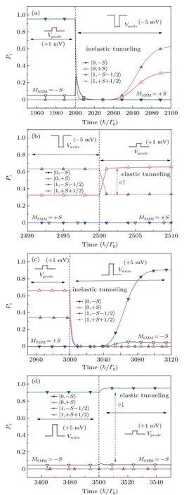
Fig. 3. The time-dependent probabilities of SMM states from Vprobe to Vwrite(+S), from Vwrite(+S) to Vprobe, from Vprobe to Vwrite(−S), and from Vwrite(−S) to Vprobe are shown in panels (a)–(d), respectively. The dashed lines(red or blue)in panels(b)and(d)represent the spin tunneling processes between states|1,±S±1/2〉and|0,±S〉.
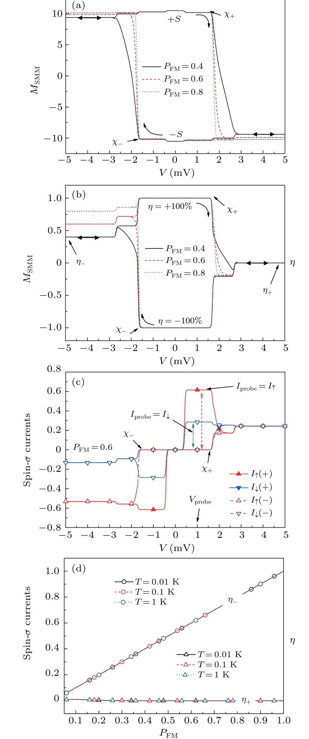
Fig.4. The hysteresis loops of the SMM’s polarization and spin-polarization coefficient η with the bias voltage scanning back and forth are plotted in panels(a)and(b), respectively. (c)The spin-σ currents(scaled by eΓ0/)with the bias scanning from −5 mV to+5 mV(solid triangle)and from+5 mV to −5 mV(hollow triangle). (d)Spin-polarization coefficient η± in the large bias regime against the spin-polarization of FM lead PFM for different temperatures.

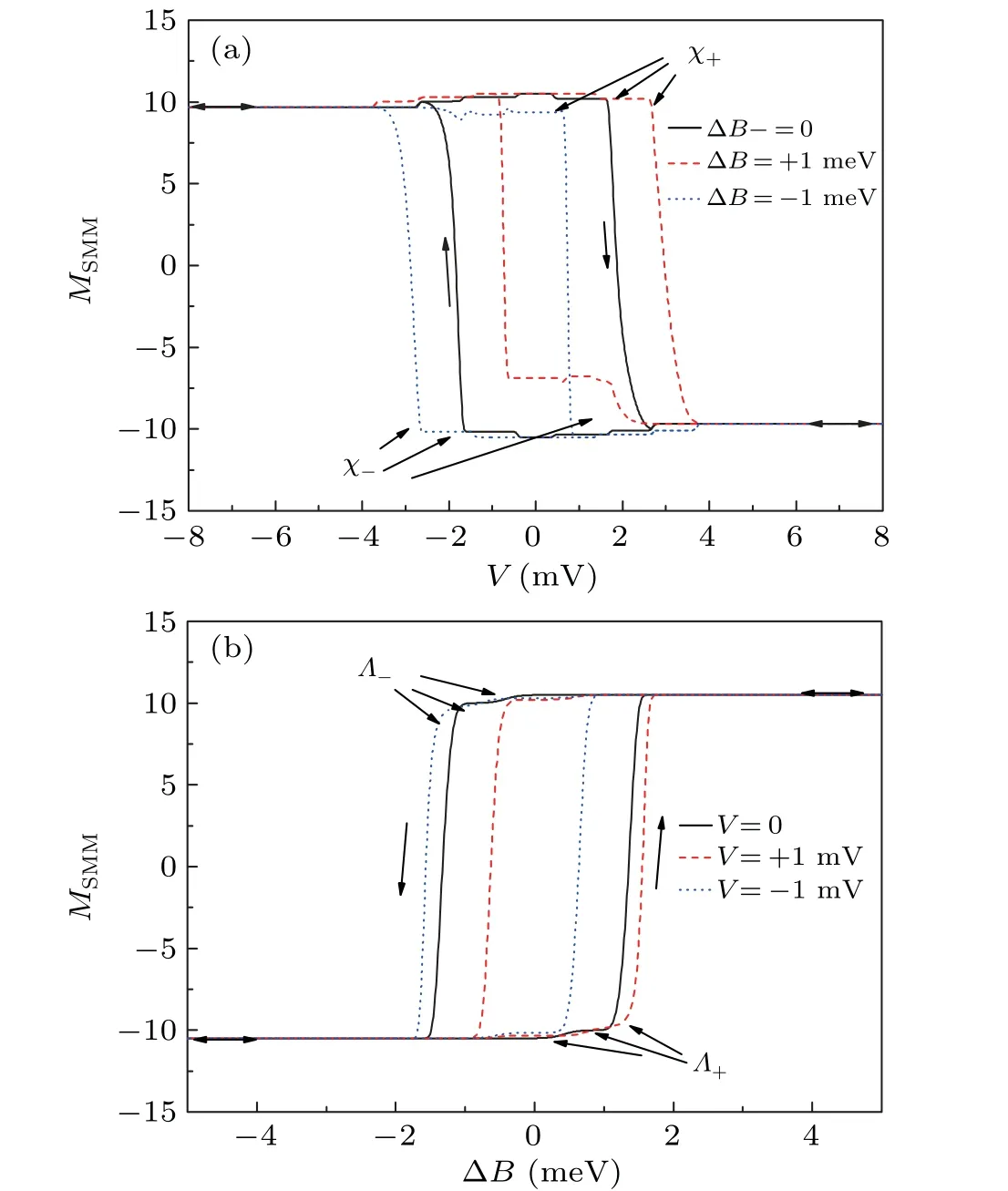
Fig.5. (a)Magnetic hysteresis loops of SMM for different external magnetic fields ∆B,with bias voltage scanning back and forth. (b)Magnetic hysteresis loops of SMM for different bias voltages,with ∆B scanning back and forth.

Fig.6. Panel(a)shows the applied voltage pulse. The tunneling currents(scaled by eΓ0/),spin-polarization coefficient η,and the polarization of SMM responding to the voltage pulse with different external magnetic fields and PFM=0.7 are shown in panels(b)–(d),respectively. The temperature is taken at T =0.5 K.
In Fig. 6, it is demonstrated the process of writing and reading out spin states of an SMM-MTJ under small magnetic fields. When ∆Bchanges from +0.5 meV to−0.5 meV, the high/low magneto-resistance switch as well as extremely high spin-polarized current can still be detected byVprobe=1 mV.Note that, for theB=−0.5 meV in Fig. 6(c) the polarization coefficientηcannot reach 100%, which means purely spin-polarized current cannot be obtained at this regime. It is because the magnetic field ∆B=−0.5 meV will make SMM’s magnetization more easily turns to−Sdirection. In Fig. 6(d), we can see the magnetization of SMM at this regime cannot keep exactly atMSMM=10 but approximately atMSMM≈8. As a result,besides the transition between|0,S〉and|1,S+1/2〉,other states such as|1,S−1/2〉and|0,S−1〉will take part in the transition process and the spin-down electrons can tunnel through the junction in this ∆Bregime.
4. Conclusion
In summary, we theoretically investigate the tunneling process in an FM/SMM/NM heterostructure. By applying different bias pulse, the polarization of SMM can be controlled parallel or anti-parallel to the polarization of the FM layer, and the high and low magneto-resistances can be obtained. Such HR–LR switching can be read out by a relatively lower bias voltageVχ+<Vprobe<Vχ+. Furthermore,extremely high spin-polarized currents withη=±100% can be readily generated in a suitable window ofVprobe,no matter what the external magnetic field and the polarization of FM lead are chosen. This scheme is fully electrically controlled and is robust against the external magnetic field or FM lead.Our scheme demonstrates that the polarization of SMM can be reversed by the spin-transfer torque. The present device is a good candidate for future spintronic devices,e.g., the biaspulse-controlling spin memory or spin generator.
- Chinese Physics B的其它文章
- Quantum computation and simulation with vibrational modes of trapped ions
- ℋ∞state estimation for Markov jump neural networks with transition probabilities subject to the persistent dwell-time switching rule∗
- Effect of symmetrical frequency chirp on pair production∗
- Entanglement properties of GHZ and W superposition state and its decayed states∗
- Lie transformation on shortcut to adiabaticity in parametric driving quantum systems∗
- Controlled quantum teleportation of an unknown single-qutrit state in noisy channels with memory∗

