Tuning transport coefficients of monolayer MoSi2N4 with biaxial strain∗
Xiao-Shu Guo(郭小姝) and San-Dong Guo(郭三栋)
1School of Electronic Engineering,Xi’an University of Posts and Telecommunications,Xi’an 710121,China
2Key Laboratory of Advanced Semiconductor Devices and Materials,Xi’an University of Posts and Telecommunications,Xi’an 710121,China
Keywords: MoSi2N4,electronic transport,2D materials
1. Introduction
The successful exfoliation of graphene[1]induces increasing attention on two-dimensional (2D) materials. Many of them have semiconducting behavior, which has various potential applications in electronics, optoelectronics and piezoelectronics.[2–5]Their electronic structures, heat transport and piezoelectric properties have been widely investigated.[6–16]It has been proved that the strain can effectively tune electronic structures, transport and piezoelectric properties of 2D materials,[15–23]which shows great potential for better use in the nanoelectronic,thermoelectric and piezoelectric applications.For example,both compressive and tensile strains can induce the semiconductor-to-metal transition in monolayer MoS2.[17]In many monolayers of transition metal dichalchogenides (TMD), the power factor can be enhanced by strain due to bands converge.[15,16,18]With increased tensile strain, the lattice thermal conductivity shows monotonous decrease, up-and-down and jump behavior with similar penta-structures.[19]Strain can also improve the piezoelectric strain coefficient by tuning the elastic and piezoelectric stress coefficients.[20–23]
Recently, the layered 2D MoSi2N4and WSi2N4have been experimentally achieved by chemical vapor deposition (CVD).[24]The septuple-atomic-layer MA2Z4monolayers with twelve different structures are constructed by intercalating MoS2-type MZ2monolayer into InSe-type A2Z2monolayer.[25]The 66 thermodynamically and dynamically stable MA2Z4structures are predicted by the first principle calculations. They can be commonly semiconductors,half-metal ferromagnetisms or spin-gapless semiconductors(SGSs), Ising superconductors and topological insulators,which depend on the number of valence electrons.[25]We predict intrinsic piezoelectricity in monolayer MA2Z4,[26]which means that MA2Z4family may have potential application in piezoelectric field. Structure effect on intrinsic piezoelectricity in monolayer MSi2N4(M=Mo and W)has also been reported by the first principle calculations.[27]By applied strain,the VSi2P4monolayer undergoes ferromagnetic metal(FMM)to SGS to ferromagnetic semiconductor (FMS) to SGS to ferromagnetic half-metal (FMHM) with increasing strain.[28]Some materials of MA2Z4lack inversion symmetry with a strong SOC effect, which are expected to exhibit rich spinvalley physics.[25]The valley-dependent properties of monolayer MoSi2N4, WSi2N4and MoSi2As4have been predicted by the first-principles calculations.[25,29,30]Recently,Janus 2D monolayer in the new septuple-atomic-layer 2D MA2Z4family has been achieved,[31]which shows Rashba spin splitting and out-of-plane piezoelectric polarizations.
In nanoscale devices,the residual strain usually exists in real applications.[32]In our previous work,the small strain effects(0.96 to 1.04)on piezoelectric coefficients of monolayer MoSi2N4have been investigated.[26]In this work, the large(0.90 to 1.10) biaxial strain-tuned electronic structures and transport coefficients of monolayer MoSi2N4are studied by the first principle calculations. Witha/a0from 0.90 to 1.10,the energy band gap of monolayer MoSi2N4firstly increases,and then decreases. In n-type doping,the Seebeck coefficientScan be effectively enhanced by applying compressive strain,and then theZTecan be improved. The tensile strain can induce flat valence bands around theΓpoint near the Fermi level, producing large p-typeS. Therefore, our works give an experimental proposal to improve transport coefficients of monolayer MoSi2N4.
The rest of the paper is organized as follows. In Section 2,we give our computational details and methods about transport coefficients. In Sections 3 and 4, we present the main results of monolayer MoSi2N4about strain-tuned electronic structures and transport coefficients. Finally, we present our conclusions in Section 5.
2. Computational detail
To avoid interactions between two neighboring images,a vacuum spacing of more than 32 ˚A along thezdirection is added to construct monolayer MoSi2N4. The elastic stiffness tensor elementsCi jare calculated using strain-stress relationship(SSR),which are performed by employing the VASP code[33,35,38]within the framework of DFT.[36,37]A kinetic cutoff energy of 500 eV is adopted, and we use the popular generalized gradient approximation of Perdew, Burke and Ernzerh of (GGA-PBE)[37]as the exchange–correlation potential to calculate elastic and electronic properties. The total energy convergence criterion is set to 10−8eV, and the Hellmann–Feynman forces on each atom are less than 0.0001 eV·˚A−1. The Brillouin zone (BZ) sampling is obtained using a Monkhorst–Pack mesh of 15×15×1 for elastic constantsCi j. The 2D elastic coefficientsC2Di jhave been renormalized by the the length of unit cell alongzdirection(Lz):C2Di j=LzC3Dij.
The electronic transport coefficients of MoSi2N4monolayer are calculated by solving the Boltzmann transport equations within the constant scattering time approximation (CSTA), which is performed by the BoltzTrap[39]code.To include the SOC, a full-potential linearized augmentedplane-waves method is used to calculate the energy bands of MoSi2N4monolayer, as implemented in the WIEN2k package.[40]To attain accurate transport coefficients, a 35×35×1k-point meshes is used in the first BZ for the energy band calculation,make harmonic expansion up tolmax=10 in each of the atomic spheres,and setRmtkmax=8.
3. Electronic structures
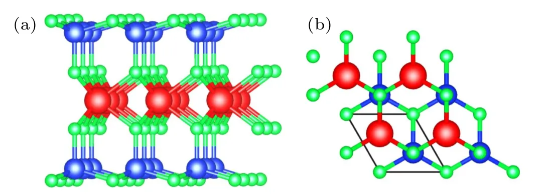
The MoSi2N4monolayer can be considered as the insertion of the 2H MoS2-type MoN2monolayer into theα-InSetype Si2N2,and the side and top views of the structure of the MoSi2N4monolayer are plotted in Fig.1.The structure breaks the inversion symmetry,but preserves a horizontal mirror corresponding to the plane of the Mo layer. This leads to that MoSi2N4monolayer only has in-plane piezoelectric response,and has not out-of-plane piezoelectric polarizations. Using optimized lattice constants,[26]the energy bands of MoSi2N4monolayer using GGA and GGA+SOC are shown in Fig. 2,and exhibit both the indirect band gaps with valence band maximum (VBM) atΓpoint and CBM atKpoint. Due to lacking inversion symmetry and containing the heavy element Mo,there exists an SOC induced spin splitting of about 0.13 eV near the Fermi level in the valence bands atKpoint. This may provide a platform for spin-valley physics,[25,29,30]but the VBM is not atKpoint,which can be tuned by strain. According to orbital projected band structure,it is found that the states near the Fermi level are dominated by the Mo d orbitals.More specifically, the states around both CBM and VBM are dominated by the Modz2orbital.

Fig.1. The crystal structure of monolayer MoSi2N4 ((a)side view and(b) top view). The primitive cell is are marked by black line, and the large red balls represent Mo atoms, and the middle blue balls for Si atoms,and the small green balls for N atoms.
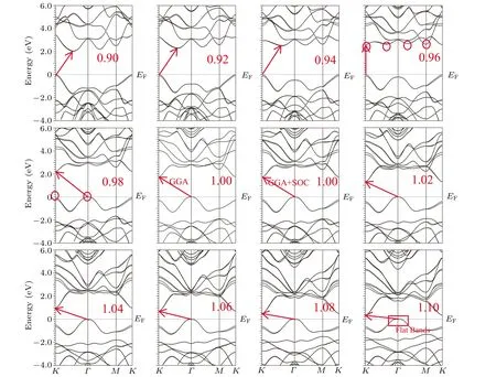
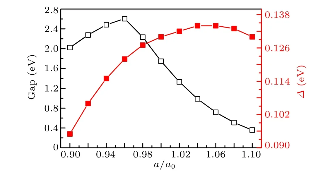
It is proved that the electronic structures, topological properties, transport and piezoelectric properties of 2D materials can be effectively tuned by strain.[15–23,41]The biaxial strain can be simulated bya/a0or(a−a0)/a0,whereaanda0are the strained and unstrained lattice constants, respectively.Thea/a0<1 or (a −a0)/a0<0 means compressive strain,whilea/a0>1 or(a−a0)/a0>0 implies tensile strain. Witha/a0from 0.90 to 1.10, the energy band structures are plotted in Fig.2,and the energy band gap and spin-orbit splitting value∆atKpoint are shown in Fig.3.

Fig.2. The energy band structures of monolayer MoSi2N4 using GGA+SOC with the application of biaxial strain(−10%to 10%),and the unstrained energy band using GGA.The VBM and CBM are marked by arrows. At 0.96(0.98)strain,four CBE(two VBE)are marked by ellipse.

Fig. 3. For MoSi2N4 monolayer, the energy band gap and spin-orbit splitting value ∆at K point using GGA+SOC as a function of strain.
It is found that the energy band gap firstly increases(0.90 to 0.96), and then decreases (0.96 to 1.10), which is due to transformation of CBM.Similar phenomena can be observed in many TMD and Janus TMD monolayers.[16,44]With strain from compressive one to tensile one, the∆has a rapid increase, and then a slight decrease. With increasing compressive strain(1.00 to 0.90),the position of CBM(VBM)changes fromK(Γ) point to one point along theK–Γdirection (Kpoint),when the compressive strain reaches about 0.94(0.96).The compressive strain can also tune the numbers and relative positions of valence band extrema(VBE)or CBE.For example,at 0.96,the four CBE can be observed,and their energies are very close, which has very important effects on transport properties. To explore orbital contribution to the conduction bands in the case of 0.96 strain,we project the states to atomic orbitals at 0.96 strained and unstrained conditions, which are shown in Fig. 4. At 0.96 strain, the composition of the lowenergy states has little change with respect to unstrained one.At 0.98, the energy of two VBE are nearly the same. The compressive strain can makeKpoint with spin splitting become VBM, which is very useful to allow spin manipulation for spin-valley physics. For example,at 0.94 strain,the VBM atKpoint is 0.49 eV higher than that atΓpoint. It is clearly seen that the increasing tensile strain can make valence band around theΓpoint near the Fermi level more flat.
Finally,the elastic constantsCijare calculated as a function ofa/a0to study the mechanical stability of MoSi2N4monolayer with strain. For 2D hexagonal crystals, the Born criteria of mechanical stability[45](C11>0 andC66>0)should be satisfied. The calculatedC11andC66as a function of strain are plotted in Fig. 5, and it is clearly seen that the MoSi2N4monolayer in considered strain range is mechanically stable,which is very important for farther experimental exploration.

Fig.4. For MoSi2N4 monolayer,the orbital projected band structure at 0.96 strained and unstrained conditions.

Fig. 5. For MoSi2N4 monolayer, the elastic constants C11 and C66 vs.a/a0 from 0.90 to 1.10.
4. Electronic transport property
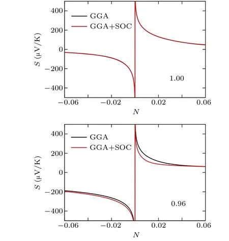
Proposed by Hicks and Dresselhaus in 1993,[42,43]the potential thermoelectric materials can be achieved in the lowdimensional systems or nanostructures. The dimensionless figure of merit,ZT=S2σT/(κe+κL),can be used to measure the efficiency of thermoelectric conversion of a thermoelectric material, whereS,σ,T,κe, andκLare the Seebeck coefficient,electrical conductivity,working temperature,electronic and lattice thermal conductivities,respectively.It is noted that,for the 2D material,the calculatedσ,κeandκLdepend onLz(here,Lz= 40 ˚A), and theSandZTis independent ofLz.For 2D materials, we use electrons or holes per unit cell instead of doping concentration, which is described byN, and theN <0(N >0)mean n-type(p-type)doping. It is proved that the SOC has important effects on transport coefficients of TMD and Janus TMD monolayers.[16,18,44]However,the SOC has neglectful influences on transport properties of unstrained MoSi2N4monolayer,which can be observed from typical Seebeck coefficientSin Fig.6.
This is because the energy bands near the Fermi level between GGA and GGA+SOC are nearly the same. However,the SOC has an important effect on p-type transport coefficients under the condition of compressive strain. For example,at 0.96 strain, a detrimental effect on Seebeck coefficientScan be observed, when including SOC (see Fig. 6). This is because the SOC can remove the band degeneracy near the VBM. Thus, the SOC is included to investigate the biaxial strain effects on transport coefficients of MoSi2N4monolayer.

Fig.6. For MoSi2N4 monolayer,the room-temperature Seebeck coefficient S using GGA and GGA+SOC at 1.00 and 0.96 strains as a function of doping level N with N being the number of electrons or holes per unit cell.

An upper limit ofZTcan be measured byZTe=S2σT/κe, neglecting theκL. The room-temperatureZTeof MoSi2N4monolayer under different strains as a function of doping level is also shown in Fig. 7. The calculated results show that the dependence ofZTeis very similar toS(absolute value),which can be explained by the Wiedemann–Franz law:κe=LσT(Lis the Lorenz number). Then theZTecan be reformulated byZTe=S2/L. Thus, the strain-induced bands convergence improvesS,which is beneficial to betterZTe.

Fig.7.For MoSi2N4 monolayer,the room-temperature transport coefficients with the a/a0 from 0.90 to 1.10,i.e.,Seebeck coefficient S,electrical conductivity with respect to scattering time σ/τ,power factor with respect to scattering time S2σ/τ and ZTe (an upper limit of ZT)as a function of doping level N using GGA+SOC.Left: compressive strain. Right: tensile strain.
5. Conclusion
In summary,we have investigated the biaxial strain(0.90 to 1.10) effects on electronic structures and transport coefficients of monolayer MoSi2N4by the reliable first-principles calculations. With the strain from 0.90 to 1.10, the energy band gap of MoSi2N4monolayer shows a nonmonotonic behavior. It is found that the SOC has little effects on transport coefficients of unstrained MoSi2N4in the considered doping range due to the hardly changed dispersion of bands near the Fermi level. However,the SOC has very important influences on transport properties of strained MoSi2N4,for example,0.96 strain, which is due to the position change of VBM.The calculated results show that compressive strain can tune the numbers and relative positions of CBE,which can lead to enhanced n-typeS,and then better n-typeZTe.Our work may provide an idea to optimize the electronic structures and transport properties of monolayer MoSi2N4.
Acknowledgments
We are grateful to the Advanced Analysis and Computation Center of China University of Mining and Technology(CUMT)for the award of CPU hours and WIEN2k/VASP software to accomplish this work.
- Chinese Physics B的其它文章
- Coarse-grained simulations on interactions between spectrins and phase-separated lipid bilayers∗
- Constraints on the kinetic energy of type-Ic supernova explosion from young PSR J1906+0746 in a double neutron star candidate∗
- Computational model investigating the effect of magnetic field on neural–astrocyte microcircuit∗
- Gas sensor using gold doped copper oxide nanostructured thin films as modified cladding fiber
- Exact explicit solitary wave and periodic wave solutions and their dynamical behaviors for the Schamel–Korteweg–de Vries equation∗
- Suppression of ferroresonance using passive memristor emulator

