
A 1.2 V, 3.1% 3σ-accuracy thermal sensor analog front-end circuit in 12 nm CMOS process
2021-04-08 07:32:32LiqiongYangLinfengWangJunhuaXiaoLongbingZhangandJianWang
Journal of Semiconductors 2021年3期
Liqiong Yang , Linfeng Wang, Junhua Xiao Longbing Zhang and Jian Wang
1State Key Laboratory of Computer Architecture, Institute of Computing Technology, Chinese Academy of Sciences, Beijing 100190, China
2University of Chinese Academy of Sciences, Beijing 100049, China
3Loongson Technology Corporation Limited, Beijing 100095, China
Abstract: This paper presents a 1.2 V high accuracy thermal sensor analog front-end circuit with 7 probes placed around the microprocessor chip.This analog front-end consists of a BGR (bandgap reference), a DEM (dynamic element matching) control,and probes.The BGR generates the voltages linear changed with temperature, which are followed by the data read out circuits.The superior accuracy of the BGR’s output voltage is a key factor for sensors fabricated via the FinFET digital process.Here, a 4-stage folded current bias structure is proposed, to increase DC accuracy and confer immunity against FinFET process variation due to limited device length and low current bias.At the same time, DEM is also adopted, so as to filter out current branch mismatches.Having been fabricated via a 12 nm FinFET CMOS process, 200 chips were tested.The measurement results demonstrate that these analog front-end circuits can work steadily below 1.2 V, and a less than 3.1% 3σ-accuracy level is achieved.Temperature stability is 0.088 mV/°C across a range from –40 to 130 °C.
Key words: CMOS FinFET process; microprocessor; thermal sensor; BGR; 4-stage folded
1.Introduction
Thermal sensors are widely used in multi-core large power server processors, fabricated in advanced digital process.Local self-heating and hotspots represent major obstacles to performance improvement.In order to track real-time temperature fluctuations, sensor probes are commonly placed throughout, alongside heavy load modules such as CPU cores and multi-bit high-speed IOs.One sensor core generally has several remote probes.Long-distance transmission metal lines act as heavy load connection resistors for these remote probes, which require the probe current to be as small as possible.Such sensors have several key requirements in relation to temperature accuracy, current consumption, area, and digital process production.
Resistor-based sensors[1]and ETF- (electro-thermal filter)based sensors[2]have been proposed, possessing both a modest power supply and a small area.Nevertheless, the temperature coefficient model of resistor-based sensors is incomplete,rendering them unsuitable for mass production.Moroever,the ETF (electro thermal filter) is a non-standard product from a foundry, and as such is also not flexible for the purpose of mass production.Rather than employing resistor- or ETF-based sensors, the parasitic bipolar transistor is more robust for mass production, and its temperature coefficient module is more accurate[3,4].The output voltage of a bipolar transistor exhibits a large variation when biased with low current in advanced nanometer processes; the current-mirror mismatch also increases due to sub-threshold operation.On the other hand, data readout circuits, with an analog front-end can be realized using a delta–sigma modulator with a 1-bit output signal[5,6], which is less insensitive to process variation.Thus, the output variation of the BGR circuit under low bias current represents the main obstacle to the integration and mass-production of highly accurate sensors in nanometer processes.Small area and low power consumption can be obtained via a switch-capacitor structure[7]; however, the switched capacitor creates output ripples, which increases the need for an accompanying high-accuracy data converter.Leakage based PTAT circuits also can realize low current consumption[8,9], but this only can be achieved in a low-temperature working environment.Leakage currents in these devices increase exponentially with an increase in temperature.Kamath realized a BGR which was highly accurate across a wide temperature range, via a 7 nm FinFET process, but at the expense of increased power consumption[10].
In this work, a 4-stage folded current bias structure is proposed, to increase both the BGR’s accuracy and its immunity against advanced digital process variation, with a low current bias and low power requirements.In this proposed structure, a high-accuracy BGR-based analog front-end is fabricated via 12 nm FinFET process.Test results show that a 3σ-accuracy below 3.1% is achieved.For a temperature range from–40 to 130 °C, the temperature stability is 0.088 mV/°C, which representing a good balance between high accuracy, small area, and low current consumption.
2.Basic principles and sensor architectures
A parasitic bipolar transistor-based structure is selected for the analog front-end of our thermal sensors.The base-emit-ter voltage,VBE, of a bipolar transistor under its forward-active region can be expressed using the well-known formula:

Fig.1.Architecture of a typical thermal sensor.

wherekis Boltzmann’s constant;qdenotes the electron charge,Tis the absolute temperature,Isis the transistor’s saturation current, andIbiasrepresents the transistor’s collector current, biased by its emitter for a substrate PNP transistor.
Of all the factors above,Isis strongly temperature dependent.Here,VBEhas a negative temperature coefficient of about–2 mV/°C.The extrapolatedVBE, denoted asVg0, is roughly 1.2 V at 0 K[11], which is independent of the absolute values ofIbiasandIs, enabling a one-time calibration for process variation[4].In this case,VPTATis generated from aVBEpair with ann: 1 collector-current ratio and a bipolar transistor of equal size.
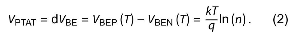
The equation above shows us thatVPTATis in positive proportion toT, so that the slope only depends on the ration,making it an accurate measure of temperature.However, temperature to data calculation still requires a constant reference voltage,VREF.As illustrated in the formula below, in order to obtain a temperature independent reference voltage,VREF, a scaled version of dVBEis added toVBE.

Fig.1 shows the architecture of a typical thermal sensor,comprising an analog front-end and an A-to-D converter.The analog front-end generates a voltage proportional to the absolute temperature (PTAT), and the A-to-D converter converts the voltage to digital information, which displays the temperature.Temperature data is determined by the ratio ofa·dVBE,which is proportional to the absolute temperature, andVREF,which refers to the complementary to absolute temperature(CTAT).Here,VREFand dVBEcan be generated indirectly though the BGR’s outputs, 2-VBE(VBEPandVBEN), operated and balanced by the ADC’s pre-operating modulator; the balance ratio ofa·dVBEandVBErepresents the final temperature output data,kdata[12]:

The above formula can be rewritten as:

TakingVBEand·dVBEas the two inputs of the ΣΔ modulator, the quantization result generated by each cycle provides the next cycle’s integrator voltage polarity.This cyclical feedback loop is intended to drive the output of the integrator to zero, so that the average value of quantization is equal tokdata.
3.Proposed analog front-end voltage generator
3.1.Problems in 12 nm FinFET process for voltage generators
The dVBEdepends only on current rationin Eq.(2), and is insensitive to process spread, but is inaccurate, due to a mismatch in the current mirror and an offset in the comparator.Here, a DEM and a chopper are used to average out this mismatch and offset.The value ofVBE, depends on the saturation and bias current values, causing it spread with process"variation.This error is often corrected by one-time calibration.The complexity and size of the calibration structure relies on the variation range and trimming resolution.Owing to considerations of test time consumption, a fixed trim code is normally used for all dies in a given wafer, so that accuracy prior to calibration is more important for a chip’s yield.Variation in the bias current can be overcome by increasing the length of CMOS devices above 1μm.Nevertheless, the 12 nm FinFET process is different from a plane Si structure, being a 3D gate structure.Finely arranged thin fins are etched onto the substrate for the source/drain region, and an arched channel is formed after oxidation and wrapped by the gate.Fin-FET structures exhibit better gate control capability and leakage performance, but suffers from severe self-heating[13], andthe channel length is limited to a maximum of 240 nm.In addition, due to the LELE (litho-etch-litho-etch) production method, adjacent graphics need to be etched twice, thus increasing the potential for local mismatch.The limited maximum length of the device causes a significant increase in DC variation and mismatch compared with normal CMOS devices.It should also be mentioned that the device’s flicker noise and the comparator’s input-offset voltage also increase, due to the device’s size limitations.

Fig.2.Analog front-end and new folded current unit.

Fig.3.(Color online) Simulation results for different numbers of folded stage used in BGR.(a) DC mismatch biased at the same current.(b) Worst variation of VBEN under 1.2 and 0.95 V, as obtained from a Monte Carlo simulation of 1000 runs.
3.2.Proposed 4-stage folded bias structure
In order to solve this problem, a 4-stage folded current bias structure,marked as 2# in Fig.2, is proposed to improve the accuracy of the BGR.Here, 4 serial PMOS transistors share the same bias voltage, in place of one current transistor (nonfolded); M4 is in the saturation region, while M1/M2/M3 operate in the linear region.Details of the transistors’ sizes are marked in Fig.2, where a maximum length of 240 nm is adopted.Additional resistors are not used, given their large area.Under the same bias conditions, a folded structure can involve larger-sized devices than a non-folded structure, reducing the current deviation caused by the device size’s limitation; M1/M2/M3 can provide about 30 kΩ, functioning as feedback source degeneration resistors, which reduces the current variation caused by supply voltage noise and threshold voltage deviation.We conducted a DC mismatch simulation of the current branch for different stage numbers under the same current and voltage bias.The normalized results are shown in Fig.3(a).The 4-stage folded structure achieves the minimum DC mismatch, which is only 26% of that for a nonfolded structure; the results for 3-stage folded and 2-stage folded structures are 35% and 54%, respectively.Subsequently,a Monte Carlo 1000-cycle trans simulation was conducted for all analog front-end circuits.The results of the worst output voltage variation are shown in Fig.3(b), decreasing dramatically as the stage number increases to 4.The worst variation in the 4-stage folded structure is only 50% of that for a normal non-folded structure.A further reduction in supply to 0.95 V,causes a slight increase in variation, but M4 is no more saturated.The stage-folded current bias structure is particularly suitable for short length FinFET processes, which greatly improve the accuracy of the analog circuits while retaining a small area.
An additional advantage of the 4-stage folded current bias structure is that it reduces the low frequency noise of the current mirrors.Flicker noise is the main low frequency noisesource.The chopper technique can help filter out the flicker noise of the current bias generation circuits, with the proviso that the device’s corner frequency is less than the modulation frequency.The chopper frequency should be as low as possible, as spikes generated by the input chopper can cause residual offset after demodulation and filtering.Offsets are generated from the charge injection mismatch of the chopper switch, impedance, and frequency.The higher the frequency used for chopping, the larger the generated offset.Therefore,a relatively low corner frequency, ideally below 100 kHz, ensures the amount of low frequency noise removed by the chopper modulator[14].Flicker noise is proportional to the dimensions of the device (including effect widthWeff, and lengthLeff).The size limitations of the FinFET device therefore constitute a drawback in terms of analog noise performance.Fig.4 shows the flicker noise simulation results for a 4-stage folded structure and a normal PMOS structure, respectively.Both circuits were simulated as having the same device size and bias current.The results show that the application of a 4-stage folded structure reduces the corner frequency by a factor of about 10.The folded method can be considered as equivalent to increasing the size of the device.

Fig.4.(Color online) Simulation results for flicker noise for normal CMOS and 4-stage folded structures.
In our analog front-end circuit design, proportional current ration= 7 is used, resulting in a temperature coefficient of 0.167 mV/°C, and the same size triodes of, 2μm ×2μm ×10, are used to generate 2-VBE.The bipolar transistor’s forward current gain independence bias structure[12]was selected to match the ‘current bias gen’ component in Fig.2, in order that the generatedVBEis independent of the current gain.Normally, the size of a large-scale processor chip is more than 10 × 10 mm2, which results in the parasitic metal wire resistors between probes and sensor core attaining values up to several kilo ohms.Here, a bias current of less than 2μA is used for the long channel probes.For each time, one of the current branches is selected as theVBEN’s current bias;the remaining seven branches are left forVBEP.Noise simulations for the entirety of the analog front-end circuit were conducted for a transistor bias and a 4-stage folded bias circuit, respectively.the case of the circuit with a normal PMOS bias structure, the PMOS biased forVBEcame at the top of the noise simulation results list, followed by the comparator’s current bias transistor, and the input differential transistors.We therefore replaced the input differential single NMOS transistors with a 2-stage folded structure, similar to #1 in Fig.2 in terms of its current bias structure.The device comprised 2 groups, totaling 16 branches of current bias, taking into account area constraints, with no further serial or parallel devices added to the folded structure.

Fig.5.(Color online) Die photo of the test chip.
3.3.Tape-out design
The proposed analog front-end and probes in Fig.2 were fabricated using 12 nm CMOS technology.Both remote and local probes used the same size BJTs, measuring 2μm × 2μm ×12.For each cycle, one of the probes is selected to be evaluated via the cluster mux.Non-overlapped clocksф1 andф2 cooperate with the modulator control to realize all current mirror branch rotation and bias generator paths’ chop.Fig.5 shows a die photo of the test chip.Except for the local one, 7 remote probes are placed all around the chip.The longest distance of the probes from the chip is more than 4800μm.
High level metal is used for the route, and the maximum parasitic resistor is about 1 kΩ.Benefitting from a bias current of less than 2μA, the IR drop for the connect wire measures less than 2 mV.According to Eq.(4), the variationbetween the different probes is less than 0.17%, based on the final temperature results.

Table 1.Comparison table.

Fig.6.(Color online) Measured variation results for 2-VBE at room temperature.
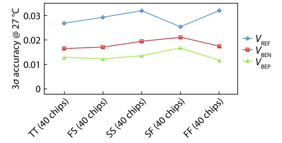
Fig.7.(Color online) 3σ accuracy statistics for 200 chips, VBEP, VBEN, and VREF.
4.Chip test and measurement statistics
Chip tests for the output voltages included a room temperature variation test, and a full temperature linear test.The chips under test consisted of 5 corners (FF, SS, TT, FS and SF).Firstly, 40 chips for each process corner were selected randomly for the room temperature variation test.A total of 200 chips’ 2-VBEwere measured, and the distributions are shown in Fig.6.The variation voltage for each corner was less than 20 mV, a difference of nearly 2.9% forVBEN, and 2.7% forVBEP.
All test results for 2-VBEand calculatedVREFwere calculated; the statistical results show that less than 3.1% 3σ accuracy was achieved for the 200 chips across the 5 corners.Here,a= 10 was used forVREFcalculation, as given in Fig.2.Detailed data distributions are provided in Fig.7.

Fig.8.(Color online) Temperature linear results for VREF (calculated by the measured results of the variations of 2-VBE).
In addition, full temperature linear tests were performed using the EFLAGS control system.By means of the chip carrier, EFLAGS can control a chip’s working temperature by rapidly cooling or heating the whole chip.Fig.8 shows the temperature variation ofVREF; the result, calculated by the measured 2-VBE, is 0.088 mV/°C in a range from –40 to 130 °C.
5.Conclusion
Table 1 compares this work with other state-of-the-artvoltage references achieving < 3.1% 3σ-accuracy over a large temperature range from –40 to 130 °C.With the proposed 4-stage folded bias structure, this BGR based analog front-end provides a ripple-free reference output voltage, while achieving competitive accuracy, together with a small area and low power consumption in a 12 nm FinFET digital process.In addition, the proposed novel structure is particularly robust, and is easily integrated for the purposes of high accuracy analog design in a FinFET process.Table 1 shows a comparison with other recently published BGR data.
Acknowledgements
This work was supported by the National Natural Science Foundation of China (No.61432016 and No.61521092),the Key Program of the Chinese Academy of Sciences (ZDRWXH-2017-1), and the Strategic Priority Research Program of the Chinese Academy of Sciences (No.XDC05020000).
 Journal of Semiconductors2021年3期
- Journal of Semiconductors的其它文章
- E nergy band adjustment of 808 nm GaAs laser power converters via gradient doping
- Side-channel attack-resistant AES S-box with hidden subfield inversion and glitch-free masking
- Resonant enhancement of magnetic damping driven by coherent acoustic phonons in thin Co2FeAl film epitaxied on GaAs
- Anomalies in Young"s modulus behavior after annealing in polycrystalline SmS
- Van der Waals heterojunction ReSe2/WSe2 polarization-resolved photodetector
- L ow-dimensional materials for photovoltaic application