
Magneto-Optical Properties of Wider Gap Semiconductors ZnMnTe and ZnMnSe Films Prepared by MBE
2020-10-19 02:21:22
Abstract—The II-VI based magnetic semiconductors with a direct and wide optical bandgap are expected to show high potential for optical applications utilizing short wavelength laser diodes (LDs),such as 532-nm green and 475-nm blue LDs.We have confirmed that the Faraday rotation θF in the ZnMnTe and ZnMnSe films deposited on quartz glass (QG) and sapphire (SA) substrates by using molecular beam epitaxy (MBE) is large near the absorption edge.This paper reports the magneto-optical properties of ZnMnTe and ZnMnSe films synthesized on the QG and SA substrates,and shows the result of a direct Faraday rotation observation successfully made for the ZnMnTe films under 1.28-kHz alternating magnetic fields.The optical absorption characteristics of the ZnMnTe films grown on the SA substrates by MBE are discussed by comparing them with the optical absorption properties and photoluminescence spectra of the II-VI ZnTe parent single crystals.
1.Introduction
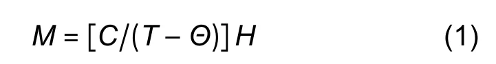
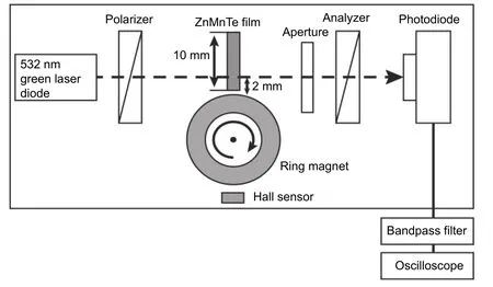
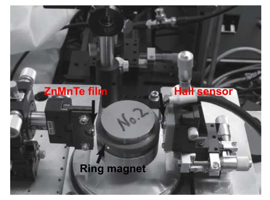
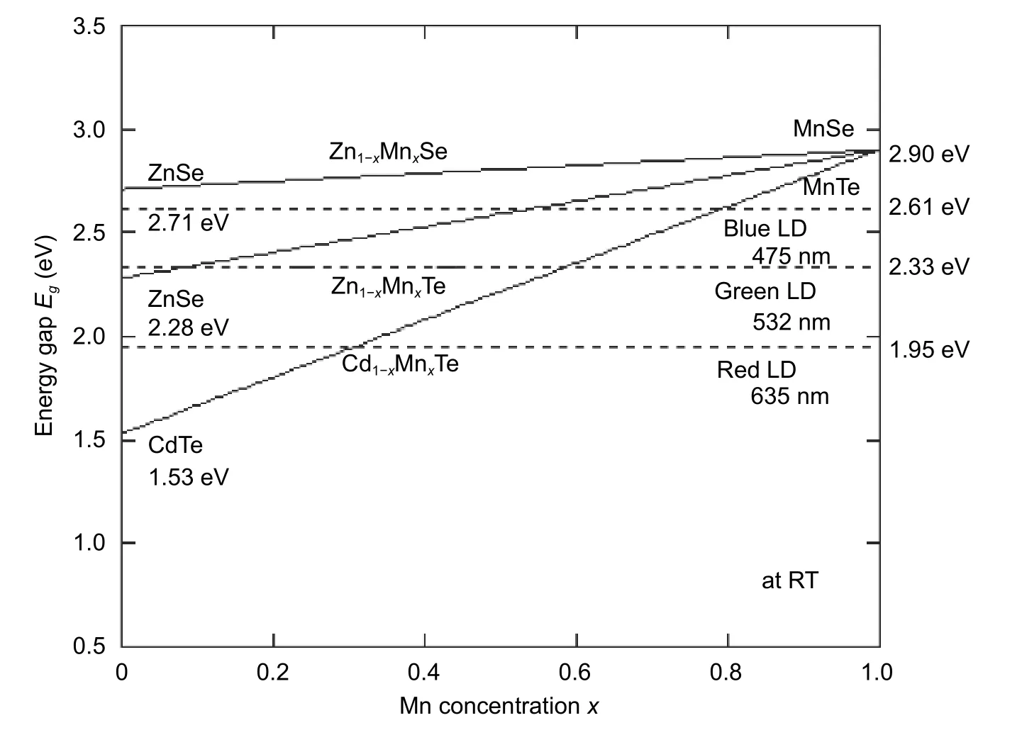
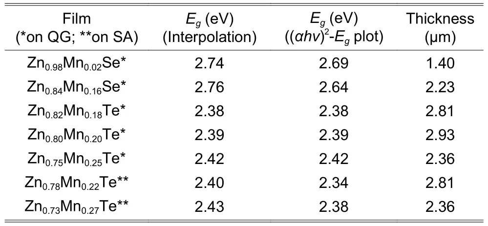
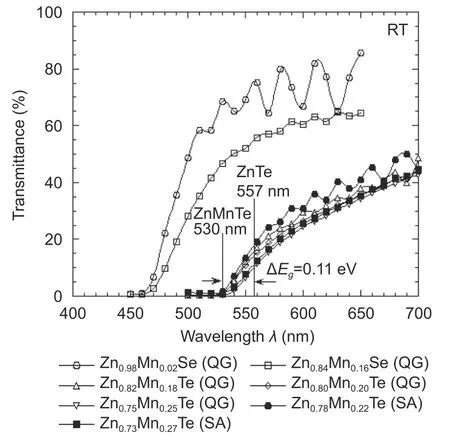
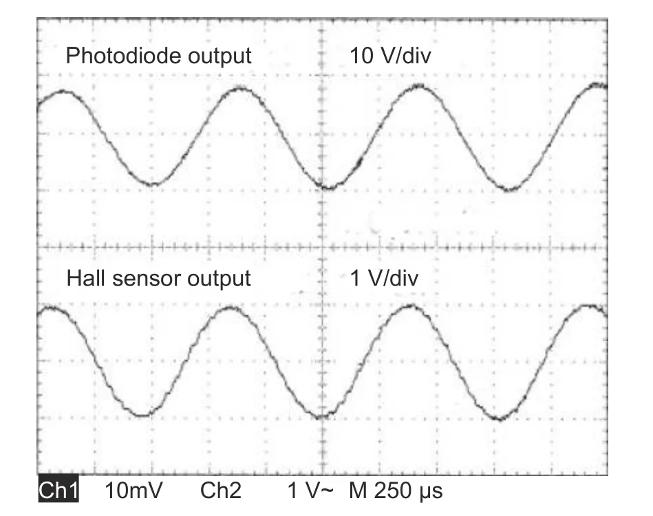
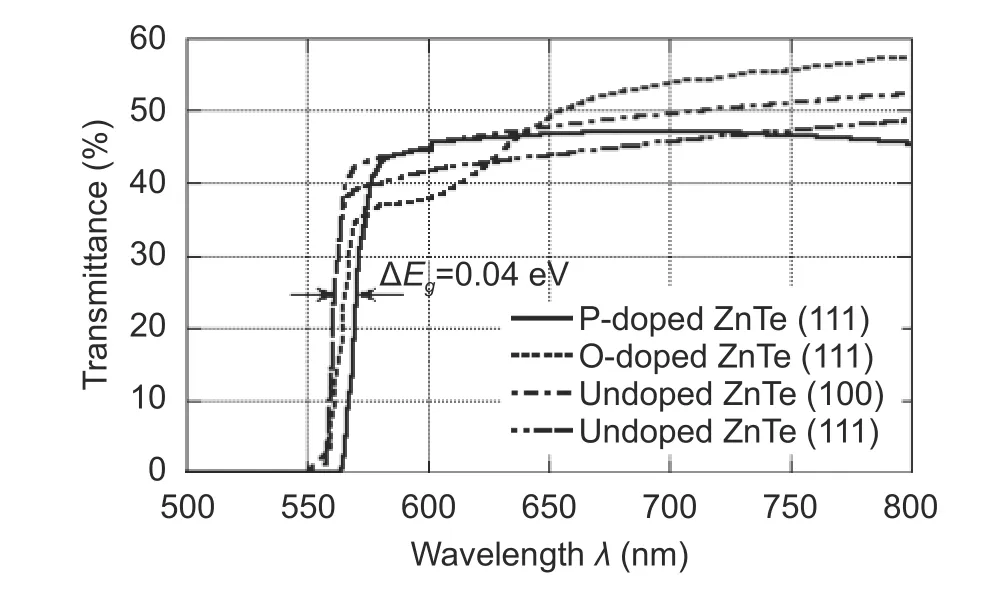
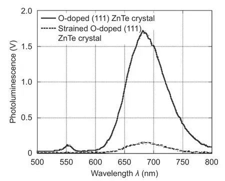
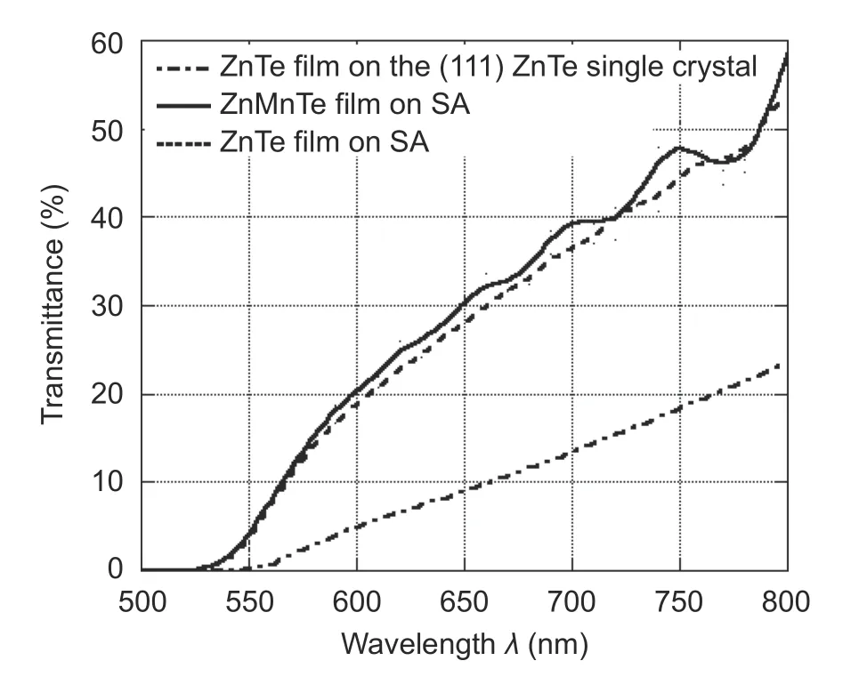
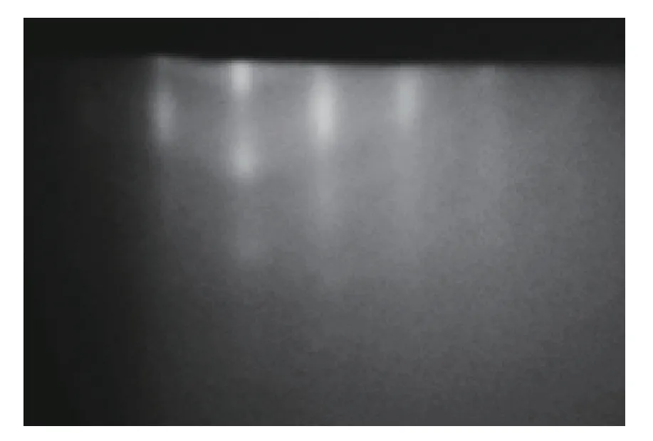
The II-VI semiconductors ZnTe crystals which do not have transition metal ions,such as Mn,have actively been studied to detect terahertz electric fields[1]-[3].Another area of intensive studies on II-VI semiconductors is the field of quantum engineering which includes heterojunctions[4],[5],quantum wells (2D structure)[6],[7],quantum wires(1D),and quantum dots (0D)[8],[9].On the other hand,the II-VI based magnetic semiconductors of thecomposition with a direct and wide optical bandgap[10],[11]show the promise for magneto-optical applications utilizing short wavelength laser diodes (LDs),such as a 532-nm green or 475-nm blue beam.The wavelengths of LDs used for high-density optical recordings have become shorter.The required optical setups need an isolator that works effectively for shortwave LDs to eliminate back reflections of the laser beam.In addition to the optical isolators,the development of magneto-optical sensors that work on a short optical wavelength has been expected[12],[13].The II-VI magnetic semiconductors Zn1–xMnxTe and Zn1–xMnxSe have the absorption edge at 428 nm to 544 nm and 428 nm to 458 nm,respectively[14].When increasing the Mn concentrationx,the shift of the absorption edge to the higher energy gap for these materials is small compared with the prototype II-VI magnetic semiconductor Cd1–xMnxTe.It will be discussed in subsection 3.1.The Faraday rotation angleθFfor the ZnMnTe films deposited on quartz glass (QG) and sapphire (SA) substrates is large near the absorption edge[15],[16].Zn1–xMnxTe forms a ternary alloy of a zinc-blende structure withxup to 0.86,and Zn1–xMnxSe exhibits a zinc-blende structure forx<0.30 and a wurtzite structure for 0.30 The specific values of the Faraday rotation in the room temperature region have not been shown for the ZnMnTe and ZnMnSe films synthesized on the QG and SA substrates by molecular beam epitaxy (MBE) so far.This fact motivated us to carry out the materials research on II-VI magnetic semiconductors.The presented paper reports the magneto-optical characteristics of those films,and describes the results of the Faraday rotations for the ZnMnTe films subject to alternating magnetic fields from a practical viewpoint of their applications. Fig.1.Schematic band structure near the Γ point for an open-gap zinc-blende magnetic semiconductor(left side) and a schematic picture of spin splitting of the top of the valence band (Γ8) and the bottom of the conduction band (Γ6) in a magnetic field (right side).The diagram shows the electric-dipole-allowed transitions(shown by arrows) for the two circular polarizations rotating transverse to the applied field (the Faraday geometry designated by σ+ and σ–).The Faraday geometry transitions marked with A and D are significantly stronger than those marked with B and C[12]. Magnetic semiconductor films were synthesized on the transparent QG and SA ((0001) orientation C-cutα-Al2O3) substrates heated to 300 °C by using MBE.Deposition was carried out at an average rate of 1.0 Å/s to 1.5 Å/s for 6 h to 8 h using a 5N ZnTe effusion cell heated to 465 °C to 475 °C and a 4N MnTe cell at 1035 °C to 1040 °C.Using this system,2-mm-thick to 3-mm-thick ZnMnTe films with the Mn mole-fractionxfrom 0.18 to 0.27 were prepared on the 0.5-mm-thick QG and SA substrates.The ZnMnSe films were prepared similarly using a 5N ZnSe effusion cell heated to 640 °C to 650 °C and a 4N MnSe cell at 820 °C to 850 °C,and their magneto-optical properties were compared with those of ZnMnTe films.An X-ray diffractometer using Cu-Kαradiation and reflection high energy electron diffraction (RHEED) were used to observe crystallinity.A (111) diffraction spectrum of weak intensity was observed by the X-ray diffractometer for the ZnMnTe and ZnMnSe films deposited on the QG substrates.Fig.2 (a) shows a weak diffraction spectrum of (111) observed for the Zn0.75Mn0.25Te film deposited on the QG substrate.Although the films are considered to have a certain amount of crystallinity,RHEED that monitors the crystal growth on the surface of films during deposition showed a ring pattern which gives an indication of the polycrystalline film growth.The films were assumed to be polycrystalline grown perpendicularly to the surface of QG substrates.Fig.2 (b) shows the diffraction spectra observed in the Zn0.73Mn0.27Te film grown on the SA substrate.As shown in Fig.2 (b),the (220) spectrum of strong intensity is exhibited at 2θ=41.9°,although the quite smaller (111) diffraction peak is also observed at 2θ=25.3°.Moreover,the streaked pattern of RHEED was observed,indicating the single-crystal growth.The (220) epitaxial growth of the ZnMnTe film on SA is considered to be due to a specificface of the hexagonal (0001) C-cut α-Al2O3crystal observed at 2θ=42.65°.Fig.3 represents the crystal structure of zinc-blend.Mn is substituted for the atoms of the group II element.The group VI element,Te or Se,is arranged in the center of a tetrahedrally bonded structure.The <111>and <220>directions of the zinc-blend crystal are indicated in Fig.3. Fig.2.X-ray diffraction spectra of ZnMnTe films: (a) Zn0.75Mn0.25Te film deposited on the QG substrate and (b)Zn0.73Mn0.27Te film grown on the SA substrate. Fig.3.Zinc-blend structure.Mn is substituted for the atoms of the group II element Zn in Zn1–xMnxTe and Zn1–xMnxSe.The group VI element Te or Se is arranged in the center of a tetrahedron.The <111>and <220>directions are indicated in the zinc-blend crystal. When the concentration of Mn++is small (x<0.01),the Mn++spins have been regarded as isolated,i.e.,independent from another[17].In that case,the magnetizationMis described by the Brillouin function and,this situation leads to the Curie-Weiss law in dependence on temperature.For magnetic semiconductors of arbitraryx,the magnetizationMis not expressed by the standard Brillouin function because of the Mn-Mn interaction.In this case,Mhas been considered to be expressed by the Curie-Weiss law in the form: whereCis the Curie constant of the paramagnetic phase,Tdenotes the temperature,His the magnetic field,andΘis the Curie temperature.Fig.4 shows the magnetic properties of the ZnMnTe films observed by using a vibrating sample magnetometer.Fig.4 (a) shows the magnetization curves for the Zn0.73Mn0.27Te film measured at–173 °C (100 K) and the room temperature (RT:300 K) in the field range of ±20 kOe.Fig.4 (b) is anM-Tcurve measured for the Zn0.73Mn0.27Te film grown on the SA substrate in relation to the temperature in the range of–195 °C (77 K) to RT.When applying the Curie-Weiss law to theM-Tcurve of Fig.4 (b),the Curie temperatureΘwas calculated at about–207 °C (66 K).The ZnMnTe film is considered to be paramagnetic at RT. Fig.4.Magnetic properties of ZnMnTe films:(a) magnetization curves observed in the Zn0.73Mn0.27Te film at –173 °C(100 K) and RT (300 K) and (b) magnetization M observed in the Zn0.73Mn0.27Te film grown on the SA substrate in relation to the temperature. Atomic concentrations were determined as mole fractions through an energy dispersion spectral analysis.The thickness of the films was measured by using a Talystep profilometer.The Faraday rotation angleθFat RT was observed in the wavelength range of 460 nm to 700 nm by using a spectrophotometer. We made direct observations of the Faraday rotation for the ZnMnTe films subject to alternating magnetic fields.Fig.5 shows the equipment used for the measurement.It has a NdFeB ring magnet (with an outer diameter of 40 mm) driven by a servomotor at a 6000-rpm maximum rotation speed.The magnet has 32 poles along the periphery of the ring.Fig.6 shows the locations of the ring magnet,a film,and the Hall sensor used to obtain a reference signal.Fig.7 plots the magnetic flux distribution of the ring magnet.This equipment can produce an AC field at a maximum frequency of 1.6 kHz.The Faraday rotation of the film was measured at a point located 2 mm away from the outer periphery of the ring magnet,where the magnetic field is 620 Gauss (62 mT).532-nm,3-mW green LD was used as the light source and an avalanche photodiode as the detector.After passing through a bandpass filter,the signal from the detector was measured by a digital oscilloscope.At 532 nm,the films exhibit a negative Faraday rotation(i.e.,a counterclockwise rotation of the polarized light).On the other hand,the bare QG substrates exhibit a positive Faraday rotation.Therefore,the net signal was reduced by the substrates. Fig.5.Equipment for observing the Faraday effect under alternating magnetic fields. Fig.6.Locations of the ring magnet,a specimen film,and the Hall sensor used for getting a reference signal. Fig.7.Flux distribution for a 32-pole ring magnet. The ZnMnTe and ZnMnSe films of the zinc-blend open gap,which exhibit a Faraday transition by the Zeeman effect,are considered to be paramagnetic at RT.The magneto-optical effect (the Faraday effect) in those films is directly related to the interaction between thedelectrons of the transition metal ions and thesandpelectrons of host semiconductors.The Faraday rotation angleθFis expressed in the form[17]: whereKis a constant,χis the magnetic susceptibility,Egis the bandgap energy,is the photon energy,andlis the film thickness.The constantKis written in the form: Fig.8.Linear interpolation of Eg between the AIIBVI and MnBVI magnetic semiconductors. Table 1:Values of bandgap energy for the ZnMnTe and ZnMnSe films on the QG and AS substrates Fig.9.Transparency for the ZnMnTe and ZnMnSe films. whereF0is the oscillator strength andβ–αis thesp-dexchange constant.Equation (2) shows thatθFis large (→±∞) near the optical absorption edge. Fig.10 shows the variation of the Faraday angle with the wavelength measured at RT in the Zn1–xMnxTe and Zn1–xMnxSe films deposited on the QG and SA substrates.A negative peak value of the Faraday rotation angleθFat RT occurs near 550 nm for the Zn1–xMnxTe films that have an absorption edge at 520 nm to 530 nm,and near 450 nm for the Zn1–xMnxSe films that have an absorption edge at 450 nm to 460 nm.The Faraday rotation spectra of the Zn1–xMnxTe films are not noticeably changed when the Mn concentration is altered.The rotation angleθFmeasured for the Zn1–xMnxTe films in the wavelength range of 550 nm to 660 nm also exhibits a negative value.The substrates exhibited a small positive value of rotation.θFof the SA substrate is a fixed value of about +0.02 °/cm-G for wavelengths and that of the QG substrate is a fixed value of about +0.03 °/cm-G.The Faraday spectra in Fig.10 have had the substrate spectra subtracted off.Whereas the difference in the Mn concentration was clearly reflected toθFof the ZnMnSe films,the differences in the Mn concentration and types of substrates (QG and SA) were not clear in theθFdata observed in the ZnMnTe films.The values of the Faraday rotation angleθFdepend on the thickness of films as well as the Mn concentration.The results suggest that the Zn1–xMnxTe and Zn1–xMnxSe films can be useful for green and blue LDs,respectively. Fig.10.Faraday rotation angle versus wavelength at RT for the Zn1–xMnxTe and Zn1–xMnxSe films on the QG and SA substrates. Fig.11 plots the Faraday effect signal measured for the Zn0.82Mn0.18Te film deposited on QG using the ring magnet and 532-nm,3-mW green LD.The upper curve graphs the Faraday rotation of the film and the lower one shows a reference signal of the fields measured when a Hall element is placed near the ring magnet.The rotating ring magnet produces an alternating field of 620-Gauss amplitude at a frequency of 1.28 kHz.The angle between the polarizer and analyzer axes was approximately 10°.As seen in Fig.11,an undistorted Faraday rotation signal of 18 mVP-Phas been observed for the ZnMnTe film.The signal is attenuated by about 25% due to the opposing Faraday rotation of the 0.5-mm-thick substrates.Similar Faraday rotation signals were observed for the Zn0.80Mn0.20Te and Zn0.75Mn0.25Te films.Using the present films and equipment,the signal to noise ratio (SNR) was 40 dB.The advantage of an optical field sensor is its anti-noise properties,since the sensor does not use electrical wires. Fig.11.Faraday-effect signal observed for the Zn0.82Mn0.18Te film at a frequency of 1.28 kHz in an alternating magnetic field of 620-Gauss (62-mT) amplitude. Magnetization in the II-VI paramagnetic semiconductor films stems from spin rotations,not from domain wall motions,therefore the films respond linearly to magnetic fields.It is expected that the films will have good response at high frequencies as well.In this study,we showed that the wide-gap ZnMnTe films work efficiently for 532-nm green LDs.Although we have not confirmed the operation of the ZnMnSe films,we believe that they will be useful in green and blue laser applications. Two groups of films prepared on the QG substrates and SA ones are entirely different in crystallinity.The films on QG are basically polycrystal films deposited on the amorphous glass substrate,and those on SA are epitaxial single crystal films grown on the hexagonal crystal substrate.However,a value difference inθFbetween the ZnMnTe films on QG and the ZnMnTe films on SA could not clearly be confirmed.The result is considered to show that the magneto-optical effect is not practically influenced by the crystallinity of the magnetic films. The Faraday rotation near the absorption edge and optical transparency are in a trade-off relation.The transmittance of films decreased gradually with shortening the wavelength of light from 700 nm to the optical absorption edge as shown in Fig.9,and the decrease of transparency observed in the wavelength range of 550 nm to 700 nm for the ZnMnTe films is felt somewhat large.We evaluated the absorption characteristics of ZnTe films grown on the SA and ZnTe single crystal substrates by MBE.Those films also exhibited similar absorption characteristics to those of the ZnMnTe films at the same wavelength range of 550 nm to 700 nm.The multiple reflections of the thin ZnMnTe/ZnTe films may have concern in the decrease of transparency.On the other hand,the bulk ZnTe single crystal plate obtained from the Bridgeman crystal growth keeps high and constant transparency from 800 nm to the absorption edge as shown in Fig.A1 in the appendix[20].The optical absorption is still a subject for further study.From a practical point of view,we are interested in an unstrained ZnMnTe single crystal that is grown by using the Bridgeman method. Whereas the transmittance of the ZnMnTe films grown on the SA substrates by MBE decreased gradually with shortening the wavelength of light from 700 nm to the optical absorption edge as shown in Fig.9,the undoped ZnTe (100)/(111) and P-doped (111) single crystals with a shape of 10.0 mm in length,10.0 mm in width,and 0.5 mm in thickness kept a high and constant transmittance in that wavelength region as shown in Fig.A1.The transmittance of the O-doped ZnTe (111) single crystal is somewhat lowered near the optical absorption edge.Undoped ZnTe single crystals exhibited the photoluminescence(PL) spectrum of very low intensity at 558 nm (green) brought by a direct-gap transition at RT,and PL of very high intensity at the wavelength of 565 nm at RT was observed for the P-doped ZnTe single crystal.PL of the P-doped ZnTe has been considered to be due to a charge transition from the conduction band to the acceptor level formed by the impurity P atoms,and that transition produces PL of very high intensity[20].The observed value 0.04 eV on ΔEgindicated in Fig.A1 is considered to show the energy difference between the energy of the acceptor level and that for the top of the valence band.The O-doped ZnTe single crystal exhibits the high intensity of PL at 680 nm(red) at RT as shown in Fig.A2.The group VI element Te is partially replaced with the impurity VI element O,which has the same electron-arrangement as Te,and PL has been considered to be due to luminescence arising from the energy of the excited O atoms bound by an isoelectric trap[20].Fig.A3 shows the optical transparency of the ZnMnTe and ZnTe films grown on the SA and ZnTe single crystal substrates.In the optical wavelength range of 500 nm to 800 nm,the transparent properties of the ZnMnTe and ZnTe films on SA were almost the same,and the ZnTe films grown on the ZnTe single crystal substrates also exhibited lower transparency. Fig.A1.Optical transparency of the ZnTe single crystals measured at RT. Fig.A2.PL intensity of the unstrained and strained O-doped (111)single crystal slab samples.PL is observed at RT.The high intensity of PL observed at 680 nm (red) has been considered to be due to isoelectric trap[20]. Fig.A3.Optical transparency of the ZnMnTe and ZnTe films grown on SA and ZnTe single crystal substrates.Data was obtained at RT. Although the RHEED observation exhibited the (111) growth of the ZnTe film grown on the ZnTe substrate as shown in Fig.A4,the film looked metallic a little and was not stoichiometric in the composition of Zn and Te.Therefore,the decrease of transparency in this case (the ZnTe film grown on the ZnTe single crystal substrate) is considered to be due to an influx of excessive Zn atoms,which produces free electrons,into the film from the ZnTe substrate.Fig.A5 shows the optical transparency of the O-doped single crystal slab samples:Unpolished (unstrained) and polished (strained) to a mirror plane by using 1-μm diamond slurry.After polishing,the transmittance of the strained ZnTe single crystal drastically decreased,and the PL intensity decreased greatly as well.The decrease of the transmittance and PL intensity mostly recovered after annealing at 300 °C for 24 h in a vacuum.Two causes of the internal distortion in the films deposited on the SA crystal substrates are considered as follows:1) A lattice distortion brought by the thermal distortion in film preparation and 2) a lattice mismatch between the crystal lattice of the film and that of substrate brought through the epitaxial growth. Fig.A4.RHEED pattern:(111) growth of the ZnTe film on the ZnTe single crystal (111) substrate. Fig.A5.Optical transparency observed at RT for the O-doped (111)single crystal slab sample (10.0 mm×10.0 mm×0.5 mm):Unpolished(unstrained) and polished (strained). The authors are indebted to Dr.A.Okada from Mitsubishi Electric Corporation and Dr.S.Seto from Ishikawa National College of Technology for supporting their study on the II-VI magnetic semiconductors.
2.Experimental Procedure
2.1.Film Preparation and Measuring Equipment


2.2.AC Faraday Signal Measuring Equipment

3.Results and Discussion
3.1.Bandgap Energy and Absorption Characteristics
3.2.Faraday Rotation for ZnMnTe and ZnMnSe Films


3.3.Green Laser Application of the ZnMnTe Film at RT
4.Conclusion
Appendix
Transparent Characteristics of Bulk ZnTe Crystals at RT

Acknowledgment
 Journal of Electronic Science and Technology2020年3期
- Journal of Electronic Science and Technology的其它文章
- Call for Papers Special Section on Energy and Environmental Materials
- Numerical Analysis of Artificial Electron Heating Effects on Polar Mesospheric Winter Echoes
- Systematic Synthesis of Compressive VDTA-Based T-T Filter with Orthogonal Control of fo and Q
- MUSIC-Based Pilot Decontamination and Channel Estimation in Multiuser Massive MIMO System
- High Capacity Data Rate System:Review of Visible Light Communications Technology
- Light-Weight Selective Image Encryption for Privacy Preservation