Single event upset on static random access memory devices due to spallation,reactor,and monoenergetic neutrons∗
Xiao-Ming Jin(金晓明), Wei Chen(陈伟), Jun-Lin Li(李俊霖), Chao Qi(齐超),Xiao-Qiang Guo(郭晓强), Rui-Bin Li(李瑞宾), and Yan Liu(刘岩)
State Key Laboratory of Intense Pulsed Radiation Simulation and Effect,Northwest Institute of Nuclear Technology,Xi’an 710024,China
Keywords:neutron SRAM,SEU,cross-section
1.Introduction
Neutron-induced single event upset(SEU)on static random access memory(SRAM)device has become one of the most serious concerns of avionics in terrestrial radiation environment. This effect causes the retaining data of SRAM to degrade and even data corruption functional errors of the digital signals. Due to the scaling down of complementary metal oxide silicon(CMOS)technology and power dissipation in sub-micron and nano-scale technologies,both the transistor area and supply voltage decrease in SRAM devices.This trend comes with a substantial drop of the critical charge required to cause data upset in an individual memory cell.[1,2]Consequently,SRAM devices are very vulnerable to neutroninduced SEU effects.
Many papers of neutron-induced SEU on SRAM devices have been published. Some researchers utilized the mono-energetic neutrons to investigate the SEU effects on SRAMs. A latest paper by Lambert et al.reported that the SEU cross-section of commercial SRAM can be fitted by a Weibull function for mono-energetic neutrons from 1 MeV to 16.2 MeV.[3]Recent work by Clemente et al.showed that the 130-nm,90-nm,and 65-nm SRAM at very low bias voltage increase the SEU sensitivity to 14-MeV neutrons.[4,5]Moreover,the neutron-induced SEU sensitivity of submicron SRAMs was investigated by using mono-energetic and fission neutron beams.[6]With the scaling down of the technology node,neutron-induced SEU effects on nanometric SRAMs were studied.[7,8]The simulation approaches based on Monte-Carlo method have been widely developed to analyze the neutroninduced SEU effects.[9–13]However,with the development of semiconductor technology,there is some lack of knowledge about the comparison of the SEU effects from the latest SRAM devices to the former generations.Little literature is available about the influence of neutron-induced secondary ion species on the SEU effects.
This paper presents new neutron-induced SEU data on SRAMs from the latest nanometric technology nodes to submicron technology nodes due to spallation,reactor,2.5-MeV,and 14-MeV neutrons.We thoroughly investigate the dependence of neutron-induced SEU effects on the incident neutron spectrum,technology node,byte pattern and neutron fluence rate. We find that the low energy neutrons have a greater influence on the SEU sensitivity with the technology downscaling. Since the incident neutron spectra and technology nodes were observed to have a strong influence on the SEU effects,Monte–Carlo simulations of nuclear interactions with device architecture have been performed for comparing with the experimental results.We also find that the contributions of neutron-induced light secondary ion species exhibit a significant enhancement of the SEU cross-sections.The influence of the range and the linear energy transfer(LET)on SEU effect are compared among the secondary ion species.These findings allow us to reveal the physical mechanism,i.e.,how the incident neutron spectra influence the SEU sensitivity.
2.Experimental setup
The tested devices are six distinct SRAMs without any hardness specification.Table 1 summarizes the main features of the SRAM devices including technology generation,manufacturer,memory capacity,and nominal supply voltage.The SRAMs are manufactured by HITACHI and ISSI companies.The technology nodes cover from 40 nm to 500 nm.The test method involved loading up to the tested SRAM devices with a uniform byte pattern before irradiation and then continuously scanning each of them every five seconds for SEU errors in sequential address logic during neutron irradiation.For a single scan of each SRAM device,the logic states of all the memory cells in the tested SRAM device were monitored within about three seconds for a single scan.Tested data transfer was carried out via a test board to a personal laptop.The software in the laptop allowed periodical data record and SEU detection.

Table 1.The tested SRAM information.
The spallation neutron irradiation experiments were performed using the China spallation neutron source(CSNS)at Dongguan,Guangdong Province in China.In this facility utilized is the nuclear spallation reaction by accelerating protons of 1.6 GeV in kinetic energy and 25 Hz in repetition rate towards tungsten target to produce neutron beams.[14]This scientific facility can provide neutron spectrum very close to terrestrial neutron.Compared with the terrestrial neutron radiation experiments,CSNS can generate a high neutron fluence rate and thus provide more efficient approach to accomplishing the SEU testing.The experiments were carried out at the sample position of end station 276 m away from the tungsten target at the beam power of 20 kW.The shutter to switch off neutron beam and the auxiliary positioning frame allow us to allocate the SRAM devices in the beam center. After the shutter opens,the SRAMs are irradiated by neutron with a steady fluence rate.Figure 1 shows the neutron spectrum generated by the CSNS.The maximum neutron energy is about 200 MeV.About 54%of neutrons are less than 1 MeV,41%are in a range from 1 MeV to 20 MeV,and 5%are above 20 MeV.The neutron fluence rate in the experiment was about 1.4×10⁶n/(cm2·s).
The reactor neutron irradiation experiment was carried out by using the Xi’an pulsed reactor(XAPR)at the northwest institute of nuclear technology(NINT)in China.This scientific facility is a pool-type reactor cooled by natural circulation of water.[15]The reactor neutron spectrum provided by the XAPR is shown in Fig.1 at the power of 500 kW under steadystate operation. Neutrons above 1 MeV account for about 29%.The neutron fluence rate is about 2.7×10¹⁰n/(cm2·s).
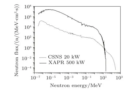
Fig.1.Neutron spectrum generated by CSNS and XAPR.
The mono-energetic neutron irradiation experiments were performed by using the 600-kV ns pulse neutron generator(CPNG)at the China institute of atomic energy(CIAE).In this facility utilized is the nuclear fusion by accelerating deuterons towards a target impregnated with either deuterium(D(d,n)3He)or tritium(T(d,n)4He)to produce mono-energetic neutrons of 2.5 MeV and 14 MeV,respectively. This facility generates 1×10⁷n/(cm2·s)for 2.5-MeV neutron and 1.4×10⁷n/(cm2·s)for 14-MeV neutron in a steady-state mode.
3.Experimental results and discussion
Three general features of neutron-induced SEU in SRAM devices are observed in the experiments.First,the total number of SEU increases linearly with neutron fluence increasing.Second,the SEU occurs once the SRAM devices are exposed to neutron irradiation.There is no threshold of neutron fluence for SEU.Third,upset bitmap is distributed uniformly in terms of logical address.The SEU cross-section is finally calculated from the following formula

where Ntotalis the memory capacity of the SRAM device,φ is the neutron fluence,and Nupsetis the SEU number. The SEU cross-section is equal to the slope of zero-crossing linear fitting of Nupset/Ntotalversus φ.The experimental research mainly focuses on the dependence of SEU cross-section on the technology node,incident neutron energy,byte pattern and neutron fluence rate.For each neutron radiation experiment,we measure four SRAM samples which are located on their respective daughter boards of the main board.The error bar of the SEU cross-section is a combination of standard uncertainty of the experimental standard deviation of the mean value and the uncertainty of the neutron fluence.
3.1.Technology node
In Fig.2,the histogram of the SEU cross-section is shown as a function of the technology node of SRAM device due to CSNS,XAPR,2.5-MeV,and 14-MeV neutrons.The experimental results show that the SEU cross-sections of SRAM devices exhibit a strong dependence on the technology node.For the technology nodes from 40 nm to 350 nm,neutron-induced SEU cross-section increases with the technology node increasing.This trend is mainly due to the strong dependence of sensitive volume and probability of ion hitting sensitive zone on the technology node.Due to the scaling down of technology,both the sensitive volume and the probability of ion hitting sensitive zone decrease. Consequently,the neutron-induced energy deposition in the sensitive volume decreases.This effect counteracts the influence of the critical charge reduction and eventually leads to a lower SEU sensitivity. The SEU cross-section of HM628512A(500 nm)is slightly higher for 2.5-MeV neutrons,but much lower for CSNS,14-MeV and XAPR neutrons than that of HM628512B(350 nm).This discrepancy is due to the deviation of the test data and the different neutron sources.
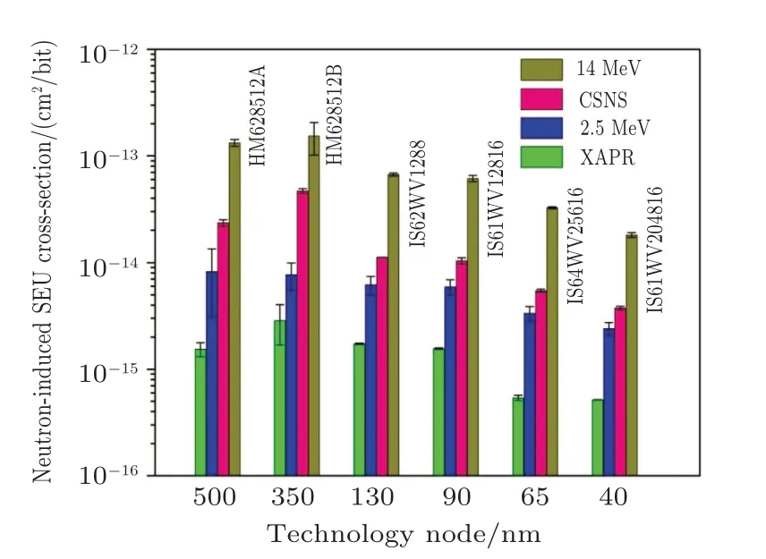
Fig.2. Neutron-induced SEU cross-section as a function of technology nodes and incident neutron spectrum.
3.2.Incident neutron spectrum
As shown in Fig.2,the neutron-induced SEU sensitivity of SRAMs also strongly depends on the incident neutron energy.For each technology node,the maximum SEU crosssection is induced by 14-MeV neutron,followed by CSNS,2.5-MeV,and XAPR neutrons.As we can see in Fig.1,CSNS produces relatively hard neutron spectrum while XAPR generates relatively soft neutron spectrum.This trend can be explained by the dependence on the secondary ions which are highly ionized and contribute to the SEU cross-section.As the energy of incident neutrons is higher,the number of open nuclear reaction channels increases. Because the cross-section of each reaction channel is a function of neutron energy,the increase of nuclear reaction cross-section leads the secondary particles to increase,and thus causing the SEU cross-section to augment.Therefore,the SEU cross-section increases with the energy of incident neutron increasing.
The experimental data imply that the SEU sensitivity induced by low-energy neutron significantly increases with the technology integration.As shown in Fig.3,with the scaling down of technology node from 350 nm to 40 nm,the SEU cross-section ratio of 2.5-MeV to 14-MeV neutrons increases from 0.05 to 0.13.According to Lambert’s neutron-induced SEU tests at CEA/DIF,these neutron threshold energy values are lower than the neutron threshold energy values obtained from older devices.[3]Both this and figure 3 demonstrate that the more advanced SRAM devices become more sensitive to low-energy neutrons.Therefore,the low energy region of terrestrial neutrons has a greater influence on the SEU crosssection with the technology downscaling. The neutron irradiation tests should offer the characterizations of SEU effects induced by low-energetic neutrons as well as high-energy neutrons.

Fig.3.SEU cross-section ratio of 2.5-MeV neutron to 14-MeV neutron as a function of technology node.
To further investigate the relationship of the ionizing dose deposit with the incident neutron energy,the kinetic energy released from material,i.e.,kerma factor,is calculated for each of CSNS,XAPR,14-MeV,and 2.5-MeV neutrons.The kerma factor describes the energy deposition per target mass and the neutron fluence. In Table 2 listed are the total,displacement,and ionization kerma factors in silicon for neutrons. For 14-MeV and 2.5-MeV neutrons,the total kerma factors are cited from Ref.[16]and the displacement kerma factors cited from Ref.[17]. The Geant4 is utilized to calculate the ionizing and non-ionizing energy losses in silicon for CSNS and XAPR neutron spectra. The ionization kerma factor is 1.16×10⁻⁹rad·cm2for 14-MeV neutron and 3.30×10⁻¹¹rad·cm2for XAPR neutron spectrum.Between them the ionization kerma factor is 1.83×10⁻¹⁰rad·cm2for CSNS neutron and 6.00×10⁻¹¹rad·cm2for 2.5-MeV neutron.Consequently,it could be qualitatively deduced that 14-MeV neutron can induce the highest SEU cross-section followed by CSNS neutron,2.5-MeV neutron,and XAPR neutron in succession.

Table 2.Total,displacement,and ionization kerma factors in silicon for neutrons.
3.3.Byte pattern
The dependence of CSNS neutron-induced SEU crosssection on technology node is investigated with different byte patterns. For different byte patterns,the storage cells in the SRAM device are initialized in different logic states at the beginning of the neutron exposure.As shown in Fig.4,the SEU cross-sections are measured to be almost identical for four types of byte patterns. These results indicate that the upset cross-section from logic 0 to 1 is the same as that from logic 1 to 0.

Fig.4.CSNS neutron-induced SEU cross-section versus technology node for four types of byte patterns.
This phenomenon can be explained by the structure of the memory cell.An SRAM device is composed of homogeneous memory cells in the physical structure and operation mode.Figure 5 shows a typical layout of an SRAM cell.Figure 5(a)illustrates a simplified expression of the SRAM cell,in which two inverters are connected as a ring. The circuit is stable when the data in both nodes are reversed,and thus can store data.More specifically,as shown in Fig.5(b),this cell is composed of 4 NMOSFETs(M1,M3,M5,and M6)and 2 PMOSFETs(M2 and M4). Word line(WL)and bit line(BL)are used to write or read the data.Two nodes Q andstore data 1(VDD)or 0.Neutron-induced SEU in the cell reverses the state of the node Q andsimultaneously.Due to the symmetry of the circuit structure and bias state,the SEU cross-section from logic 0 to 1 is completely identical to the cross-section from logic 1 to 0.Consequently,the byte patterns have no influence on neutron-induced SEU cross-section.
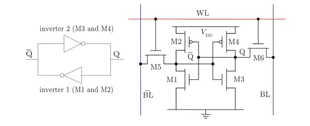
Fig.5.Circuit of SRAM cell:(a)equivalent circuit and(b)circuit of sixtransistors cell.
3.4.Neutron fluence rate
Figure 6 shows that the plots of experimental data of SEU cross-section versus neutron fluence rate at XAPR facility.The SEU cross-section of 40-nm SRAM and 65-nm SRAM are both almost constant for neutron fluence rate from 7.7×10⁸n/(cm2·s)to 2.7×10¹⁰n/(cm2·s). Similarly,the SEU cross-section of 130 nm SRAM is constant for neutron fluence rate from 7.7×10⁸n/(cm2·s)to 5.8×10⁹n/(cm2·s).The SEU cross-section of 500-nm SRAM is constant for neutron fluence rate from 5.8×10⁹n/(cm2·s)to 5.0×10¹⁰n/(cm2·s).The experimental data clearly show that none of the SEU effects of SRAM devices exhibits any dependence on neutron fluence rate from 7.7×10⁸n/(cm2·s)to 5.0×10¹⁰n/(cm2·s).This independence could be explained from the meaning of crosssection representing the bit upset probability per unit neutron fluence rate.Therefore,accelerator test at a high neutron fluence rate is applicable for predicting the SEU sensitivity at a low neutron fluence rate,provided that the time resolution of test system is good enough to detect all the upsets.
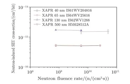
Fig.6.Plots of XAPR neutron-induced SEU cross-section versus neutron fluence rate obtained from XAPR equipped separately with four different types of SRAMs.
4.Simulations
The simulations of neutron-induced SEU are performed with Monte-Carlo toolkit Geant4.Since the experimental data show that the SEU effect only depends on the technology node and the incident neutron energy spectrum,the simulations are carried out to predict the SEU cross-sections of SRAMs from 40 nm to 500 nm for spallation neutron,reactor neutron,14-MeV,and 2.5-MeV neutrons.
4.1.Physical model
The three-dimensional topological structure of an SRAM memory cell is obtained by using the reverse-analysis technique.Figure 7 shows an example of a scanning electron microscope image from the 350-nm bulk CMOS SRAM technology.For single memory cell,the multilayer metal wirings,and passivation films over the sensitive volume are simplified by using multiple layers with equivalent thickness as depicted in Fig.8(a).The whole SRAM model is built as a matrix composed of 9×9 cells as shown in Fig.8(b).
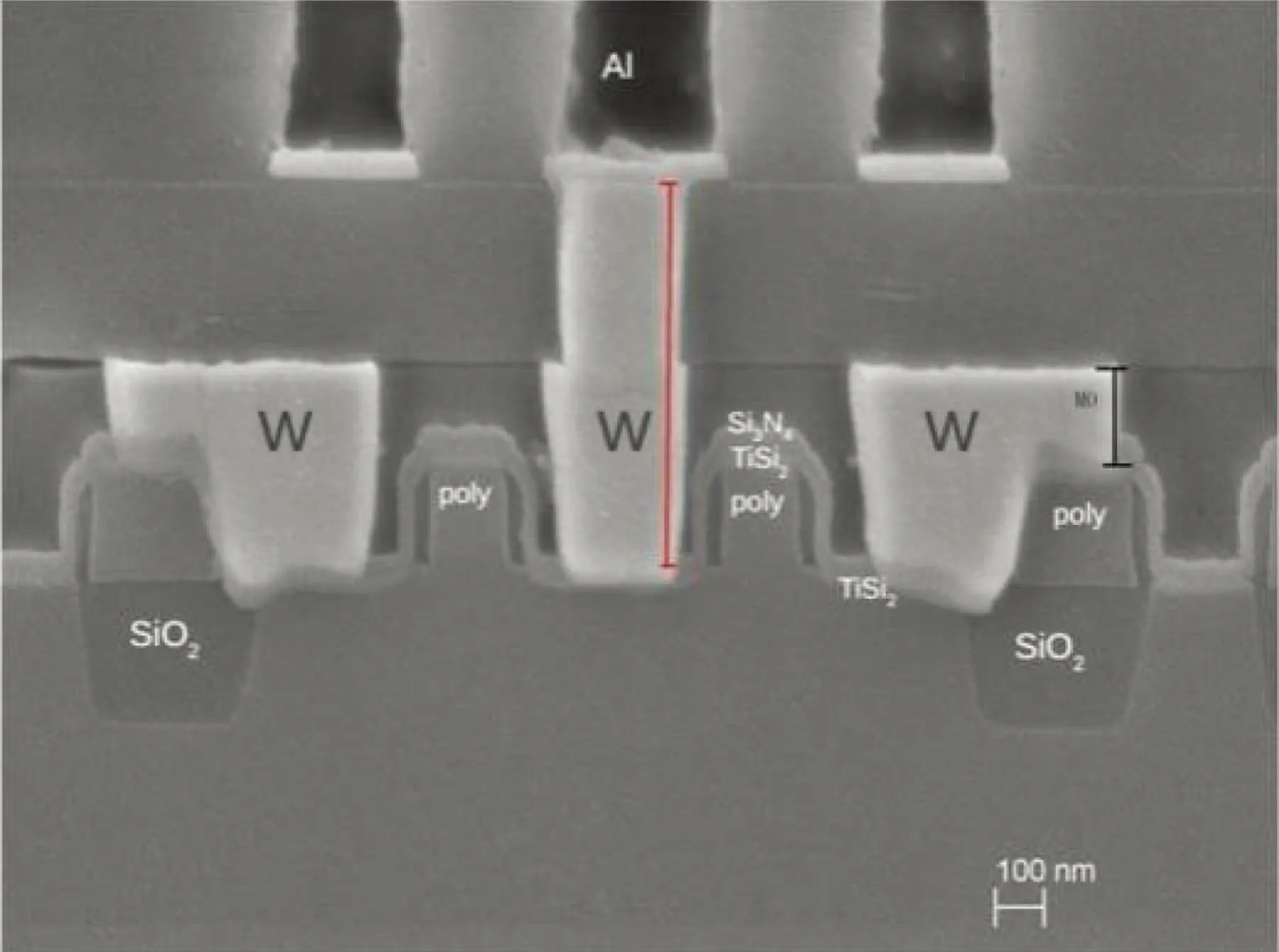
Fig.7.Scanning electron microscope cross-section by bulk CMOS SRAM technology.
This model includes the metalizations,passivations,sensitive volume,and the substrate silicon. The incident direction of primary neutron is perpendicular to the top surface of the model. The incident position of the primary neutron is sampled from a uniform distribution at the top surface.The incident energy of the primary neutron is sampled from the neutron spectrum.A comprehensive set of physics lists are established to simulate the transportation and interaction of neutron and secondary particles. The hadronic interactions are described by thethe electromagnetic effect by the G4EmStandardNR,the decay process by the G4DecayPhysics,and the neutron interaction with the
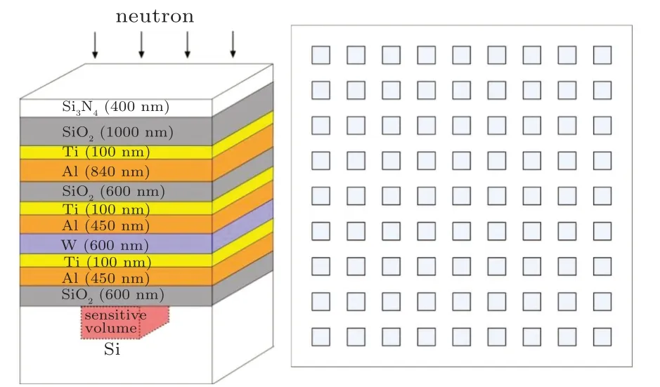
Fig.8. Geometrical model of Geant4 simulation:(a)single memory cell and(b)multiple memory cells.
The main parameters in the simulation are listed in Table 3.According to the scaling rule of the CMOS technology,the geometrical sizes of both the over-layers and sensitive volume change proportionally with the technology nodes.Used in the SEU analysis after the Geant4 simulation are two important parameters which are the critical charge and the deposited charge in the sensitive volume. The SEU criterion is based on a comparison between the critical charge quantity and the deposited charge quantity.If the deposited charge quantity exceeds the critical charge quantity,an SEU occurs,otherwise no SEU occurs.For example,a technology with a critical charge quantity of 30 fC is sensitive to every neutron that is able to deposit a charge quantity exceeding 30 fC.The calculation of the cross-section is first made by summing the number of neutrons that have deposited a charge quantity exceeding the critical charge quantity in the sensitive volume.This number is then statistically weighted and normalized with respect to the neutron fluence.
The deposited charge quantity Qdepcan be calculated from the deposited ionization energy Edepthrough the following formula:

where the two quantities Qdepand Edepare in unit C and unit eV,respectively,e is the electron charge:1.6×10⁻¹⁹C,the value 3.6 eV is the average energy to generate a hole–electron pair in silicon.
The critical charge quantities for the simulation models are also listed in Table 3. The critical charge quantity of a memory cell depends on the circuit characteristics.The critical charge quantity can be estimated by the node capacitance multiplied with the critical voltage as shown in formula(3).The critical voltage as shown in formula(4),is assumed to be about half of the supply voltage. The node capacitance as shown in formula(5),depends on the length,width,gateoxide thickness of the MOS transistor.The width and length are proportional to the size of technology node.According to the analysis above,we assume that the critical charge is proportional to the supply voltage multiplied with the square of the technology node.Furthermore,the reasonable range of the critical charge quantity is estimated according to Refs.[9]–[11]by Lambert et al.and Ref.[12]by Baggio et al.Small adjustments of the critical charge quantity have been done in order to fit the experimental results
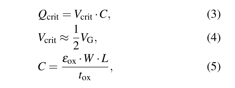
where Qcritis the critical charge,Vcritis the critical voltage,C is the node capacitance,VGis the gate voltage which is equal to the supply voltage,εoxis the dielectric constant of the oxide,W is the width of the MOS transistor,L is the length of the MOS transistor,and toxis the thickness of the MOS transistor.

Table 3.SEU simulation parameters.
4.2.Comparison between simulation and experiment
Figure 9 shows that the plots of simulated SEU cross-section versus critical charge quantity for XAPR neutrons,CSNS neutrons,2.5-MeV neutrons,and 14-MeV neutrons. The critical charge quantity is the minimum deposited charge quantity which is needed to cause an upset.According to this figure,as the critical charge quantity increases,the number of particles can deposit a charge quantity more than as the critical charge quantity decreases and the SEU cross-sections will then decrease.
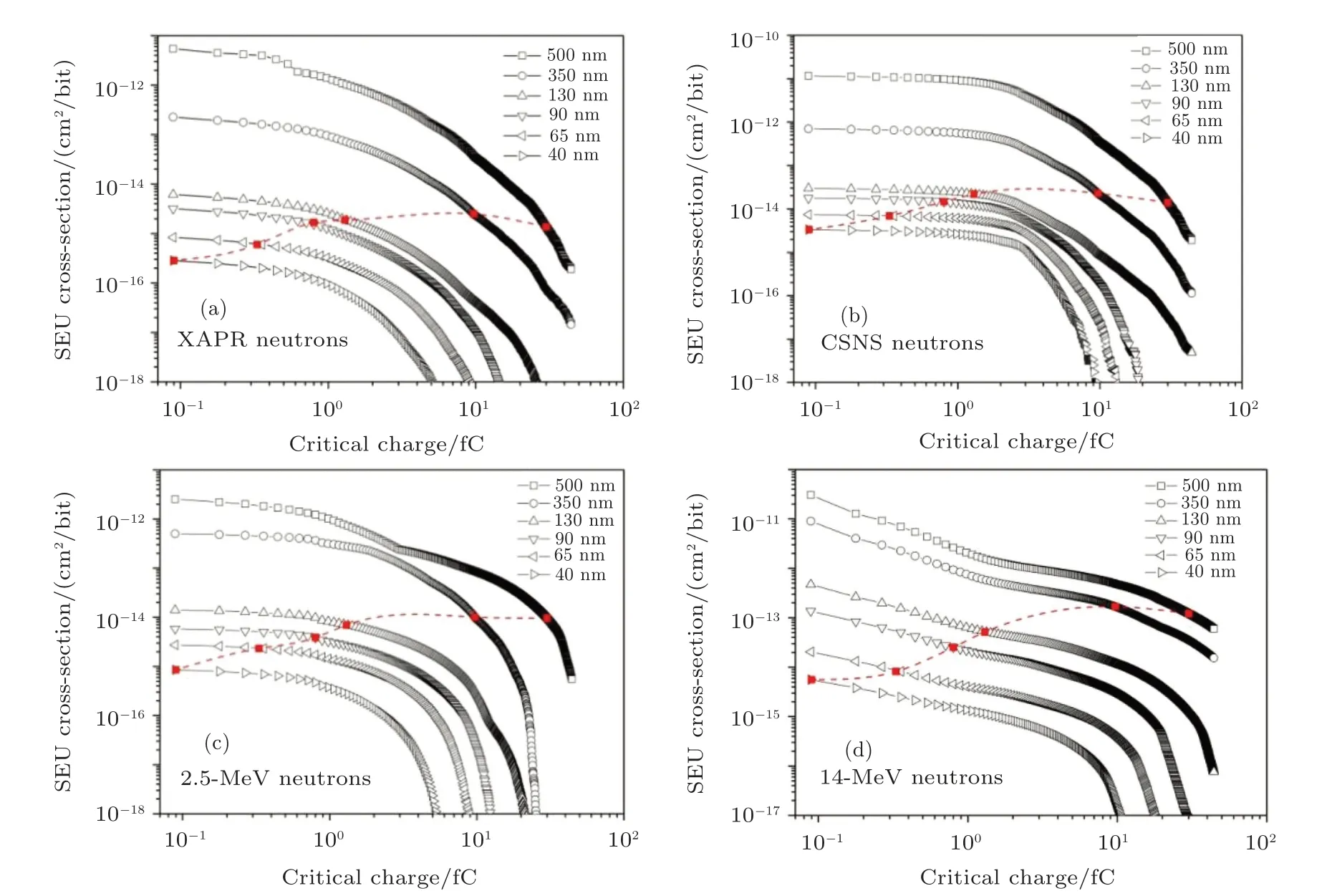
Fig.9.Plots of simulated SEU cross-section versus critical charge for four types of neutron energy:(a)XARP neutrons,(b)CSNS neutrons,(c)2.5-MeV neutrons,and(d)14-MeV neutrons.
For different technology nodes,the SEU cross-sections are determined(see red points in Fig.9)by using the critical charge quantity in Table 3. The critical charge quantity depends on not only the technology nodes but also the supply voltage. A supply voltage(3.3 V)is applied to each of the 40-nm to 350-nm SRAM devices and the critical charge quantity decreases only with the number of technology nodes.Meanwhile,the sensitive volume also decreases with the size of technology nodes decreasing,leading the deposited charge quantity to decrease in the sensitive volume.Consequently,the SEU cross-section depends on both the critical charge quantity and the deposited charge quantity in the sensitive volume.According to Fig.9,for the technology nodes from 40 nm to 350 nm,the SEU cross-sections decrease with the size of technology node decreasing.This trend indicates the influence exerted by the deposited charge quantity on the cross-section exceeds the influence by the critical charge quantity.However,the SEU cross-sections of 500 nm becomes lower than that of the 350 nm due to the higher supply voltage of 500-nm SEU(5 V)causing an overlarge critical charge quantity.
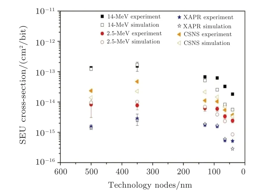
Fig.10. Comparison between simulation and experimental SEU crosssections.
The comparison between simulation and experimental results of neutron-induced SEU cross-section is shown in Fig.10.The simulated SEU cross-sections are consistent with those obtained experimentally.The deviation between simulation and experiment turns larger with the scaling down of technology nodes for 2.5-MeV neutrons,14-MeV neutrons,and XAPR neutrons.A plausible explanation of this trend is that the geometrical dimensions and the critical charges in Table 3 are not very precise only by the empirical formula,especially for 90-nm,65-nm,and 40-nm SRAM.More precise model parameters for the technology nodes less than 90 nm are needed to further improve the simulation accuracy.Moreover,the uncertainty of CSNS and XAPR neutron spectrum also lead to a discrepancy between the simulation and experiment.Although the deviation does exist,the simulated SEU cross-section decreases with the technology node size decreasing from 350 nm to 40 nm.The 14-MeV neutrons induce the maximum SEU cross-section,followed by CSNS neutron,2.5-MeV neutron,and XAPR neutron in sequence.These variation trends of SEU cross-section with incident neutron energy are in good accordance with the experimental results.
4.3.Analysis of secondary ion species
The relative contributions of secondary ion species to the total SEU are shown in Fig.11.It is quite clear that the incident neutron spectrum has a significant influence on the contribution of secondary ion species.The proton,alpha,25Mg,27Al,28Si,and16O make the main contributions to SEU for CSNS neutrons and 14-MeV neutrons,and the28Si and16O for XAPR neutrons and 2.5-MeV neutrons.The 14-MeV neutrons and CSNS neutrons could generate more kinds of secondary particles to cause SEU than the XAPR neutrons and 2.5-MeV neutrons. The simulation and experimental results show that the 14-MeV neutrons and CSNS neutrons can induce very high SEU cross-sections,which implies that the high-energy neutrons(high energy part of CSNS neutrons and 14-MeV neutrons)tend to generate both light particles(proton and alpha)and multiple types of heavy particles(25Mg,27Al,28Si,and16O)to cause ultra-high SEU sensitivity On the contrary,low-energy neutrons(XAPR and 2.5-MeV neutrons)mainly generate heavy secondary particles(28Si and16O)to cause SEU effects. The energy dependence can be further analyzed by the nuclear reaction channels and corresponding neutron threshold energy in Table 4. The high-energy neutrons have more nuclear reaction channels to generate more secondary particles.Secondary alphas and protons can be generated from the reaction between 14-MeV neutrons and all the nuclides(Si,O,N,Al,Ti,W)in the memory cell.However,for 2.5-MeV neutrons,only the reactions with N and Ti nuclides can generate alphas,and the reactions with Al and Ti nuclides can produce protons. As shown in Fig.11,alphas and protons make significant contributions to SEU especially in smallsize SRAMs for 14-MeV neutrons,but few contributions for 2.5-MeV neutrons.Since the proportion of high energy band of CSNS neutron spectrum is much higher than that of XAPR neutron spectrum,the contributions of alphas and protons by CSNS are much greater than those of alphas and protons by XAPR.
In Fig.11,the technology nodes also have an influence on the contribution of secondary ion species. For 2.5-MeV neutrons,the contribution of28Si particles to SEU tends to decrease with the technology downscaling(0.86 for 500 nm,0.82 for 350 nm,0.79 for 130 nm,0.74 for 90 nm,0.7 for 65 nm,0.63 for 40 nm).Meanwhile,the contribution of16O particles to SEU tends to increase with the technology downscaling(0.08 for 500 nm,0.12 for 350 nm,0.14 for 130 nm,0.2 for 90 nm,0.24 for 65 nm,0.31 for 40 nm).For 14-MeV neutrons,the contribution of both alphas and protons to SEU tend to increase with the technology downscaling. In large size SRAMs,the LET threshold to cause SEU is very large,and the SEU effect is thus mainly caused by heavy particles due to their high LET.In smallsize SRAM,the LET threshold to cause SEU is low,and in this case the protons and alphas can make considerable contribution.
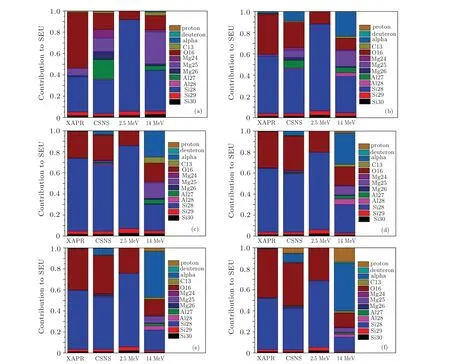
Fig.11.Contribution of secondary ion species to SEU for different neutron spectra:(a)500-nm SRAM,(b)350-nm SRAM,(c)130-nm SRAM,(d)90-nm SRAM,(e)65-nm SRAM,and(f)40-nm SRAM.
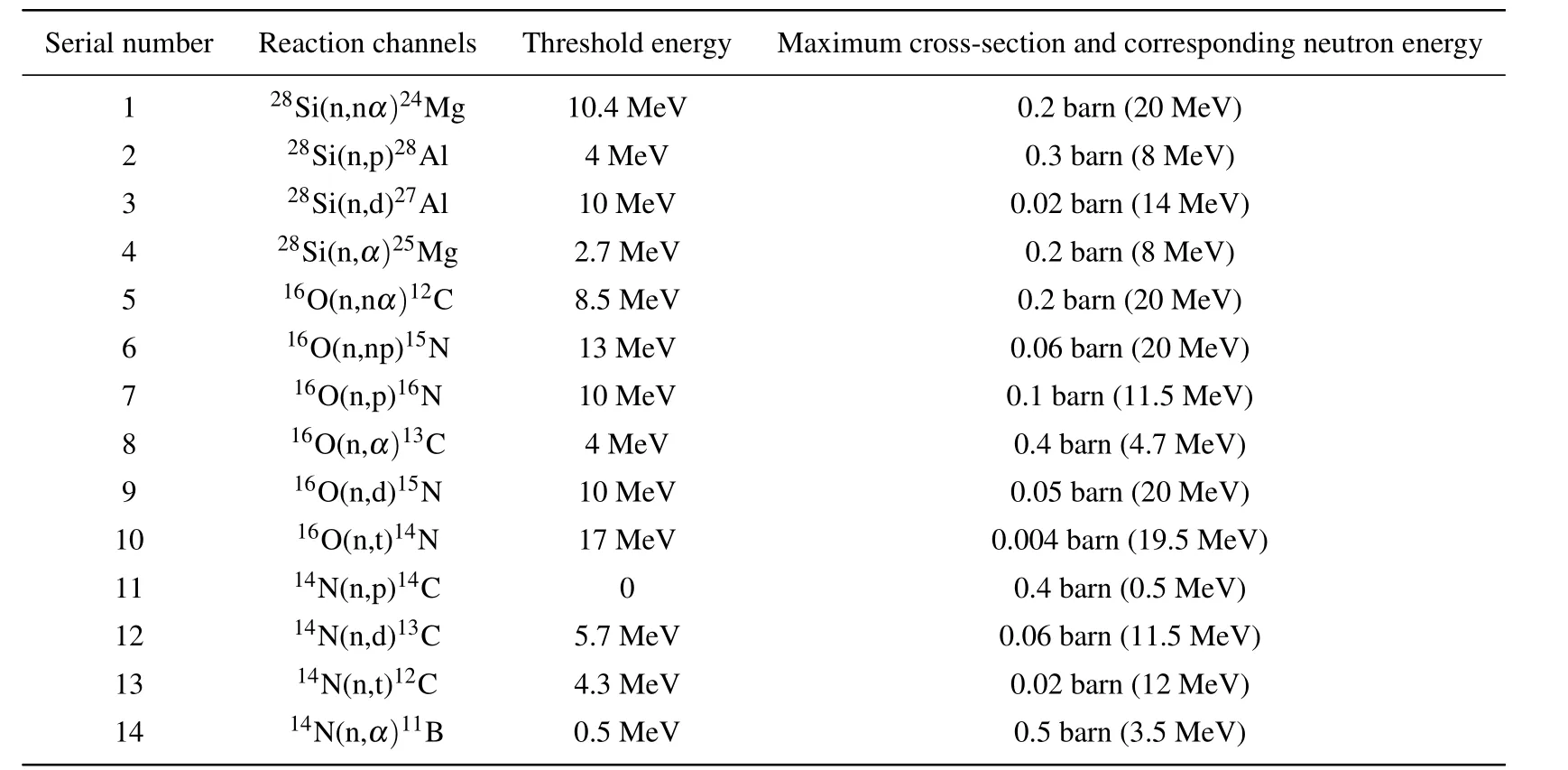
Table 4. Neutron reaction channels,threshold energy,maximum cross-sections,and corresponding neutron energy.The unit 1 barn=10−24 cm2.
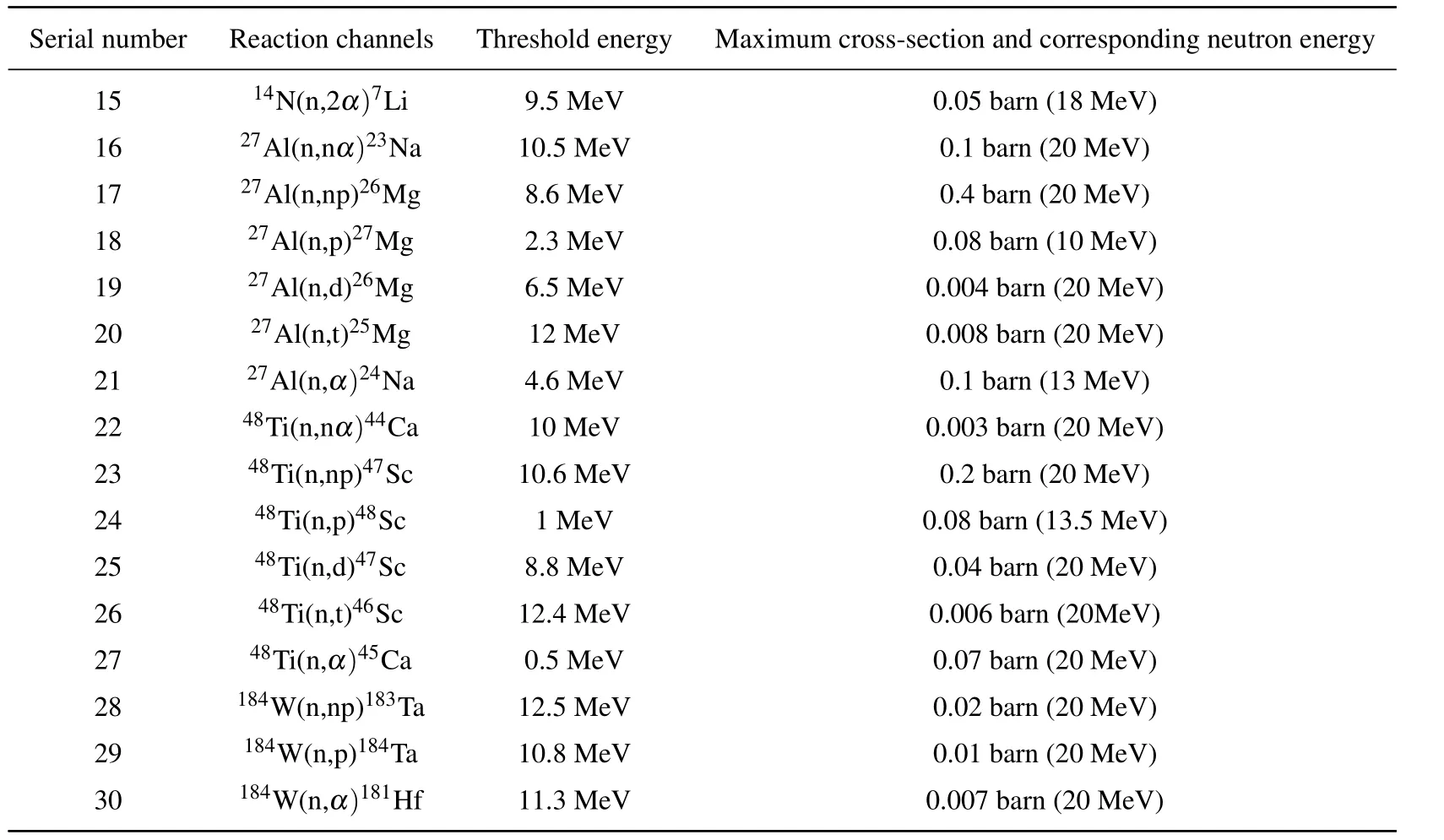
Table 4. (continued)
To in depth understand the contributions of secondary ion species to SEU effect,it is helpful to study the range and LET of the neutron-induced secondary particles. The range is an important parameter to determine whether the particle reaches the sensitive region from the position where it has been generated.Figure 12 indicates the range of secondary particles.As shown in this figure,the range of each particle increases with the energy increasing.The light particles(alpha,proton and deuteron)have a larger range than heavy particles(C,O,Mg,Al,and Si). Consequently,the light particles have a higher probability to reach the sensitive region.The LET is another important parameter to describe the energy loss of a particle per unit length and unit target mass.
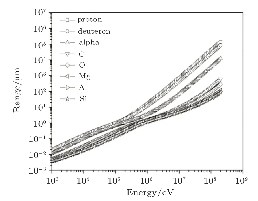
Fig.12.Range of secondary ion species versus energy in silicon.
Figure 13 shows the LET of secondary particles.For each particle,the LET first rises with its energy increasing and then begins to decline after a peak value.Compared with the light particles,the heavy particles can induce great LET in the sensitive volume.
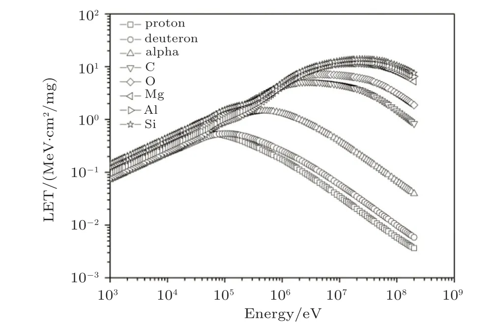
Fig.13.LET of secondary ion species versus energy in silicon.
5.Conclusions and perspectives
Spallation,reactor,and monoenergetic neutrons are utilized to experimentally study the neutron-induced SEU testing on commercial SRAMs with technology nodes from 40 nm to 500 nm.The SEU cross-section strongly depends on both the technology node size and the incident neutron energy.For the SRAMs with the technology nodes from 40 nm to 350 nm,the SEU cross-section decreases with the scaling down of technology node. The higher supply voltage enhances the critical charge quantity of the 500-nm SRAM and thus reduces its SEU cross-section to some extent.The 14-MeV neutron induces the maximum SEU cross-section,followed by CSNS neutron,2.5-MeV neutron and XAPR neutron in sequence.Kerma factors are calculated to compare the SEU sensitivities due to different neutron spectra by their ionization energy deposit.Importantly,the SEU sensitivity induced by low-energy neutron significantly increases with the technology integration.Moreover,the byte patterns of the SRAM devices have no influence on the SEU cross-section due to the symmetry of the two-inverters circuit structure and bias state. The experimental results show that the neutron fluence rate has no influence on the SEU cross-section either.
The simulation approach with Monte-Carlo toolkit Geant4 is established to analyze the neutron-induced SEU effects.The trend for each of the simulated SEU cross-sections is consistent with that of the experimental data.The geometrical dimensions of the cell area and the sensitive volume are determined by the technology nodes according to the scaling rule of the CMOS technology.The critical charge quantity is estimated by the node capacitance multiplied with the critical voltage.The geometrical dimensions and the critical charge quantity allow us to understand the mechanism of the significant influence of the evolution of technology nodes on the neutron-induced SEU sensitivity.
The SEU sensitivity difference caused by different neutron spectra can be explained by the contributions of secondary ion species to the SEU.The light particles can be generated only by the high-energy part of the incident neutrons over the threshold energy of the nuclear reactions.Compared with the heavy particles,the light particles have long range but low LET.The simulation data show that high-energy neutrons mainly generate more proton and alpha particles to cause ultrahigh SEU sensitivity,and low-energy neutrons mainly generate28Si and16O particles to cause SEU effect.Meanwhile,the technology nodes also have an influence on the contribution of secondary ion species.
The experimental and simulation data provide general trends and physical mechanism for SEU sensitivity with respect to the technology downscaling and the incident neutron energy.For hardness assurance,the SEU dependence must be taken into account through a comprehensive technology nodes and neutron spectrum qualification.Neutron irradiation tests should offer the characterizations of SEU effects induced by low-energetic neutrons as well as high-energy neutrons.
Acknowledgment
The authors would like to express sincere appreciation to the collaborators for their contributions,particularly Jing-Yu Tang and Zhi-Xin Tan at CSNS and Guang-Ning Zhu and Qiang Zhang at XAPR.
- Chinese Physics B的其它文章
- Compact finite difference schemes for the backward fractional Feynman–Kac equation with fractional substantial derivative*
- Exact solutions of a(2+1)-dimensional extended shallow water wave equation∗
- Lump-type solutions of a generalized Kadomtsev–Petviashvili equation in(3+1)-dimensions∗
- Time evolution of angular momentum coherent state derived by virtue of entangled state representation and a new binomial theorem∗
- Boundary states for entanglement robustness under dephasing and bit flip channels*
- Manipulating transition of a two-component Bose–Einstein condensate with a weak δ-shaped laser∗

