Negative transconductance effect in p-GaN gate AlGaN/GaN HEMTs by traps in unintentionally doped GaN buffer layer∗
Mei Ge(葛梅),Qing Cai(蔡青),Bao-Hua Zhang(张保花),Dun-Jun Chen(陈敦军),†,Li-Qun Hu(胡立群),Jun-Jun Xue(薛俊俊),Hai Lu(陆海),Rong Zhang(张荣),and You-Dou Zheng(郑有炓)
1The Key Laboratory of Advanced Photonic and Electronic Materials,School of Electronic Science and Engineering,Nanjing University,Nanjing 210093,China
2Department of Physics,Changji College,Changji 831100,China
3School of Electronic Science and Engineering,Nanjign University of Posts and Telecommunications,Nanjing 210023,China
Keywords:AlGaN/GaN,high-electron-mobility transistors(HEMTs),traps,negative transconductance
1.Introduction
Gallium nitride(GaN)high-electron-mobility transistors(HEMTs)are attractive for high-frequency,high-power semiconductor devices and sensor applications due to their high breakdown field,high mobility,and good thermal stability.[1,2]However,conventional AlGaN/GaN HEMTs are inherently normally-on devices because of a large amount of twodimensional(2D)electron gas(2DEG)existing at the Al-GaN/GaN interface.[3]In high-power applications with simple circuitry and system reliability,normally-off devices are highly desirable.[4]The structure with p-GaN cap layer can obtain normally-off performance by depleting the 2DEG in the interface,and has drawn increasing attention in the industry due to its large threshold voltage and low on-state resistance.[5–8]
The performances of GaN-based HEMTs can be limited by the presence of surface,bulk,and interface trap states.[9,10]More recently,the traps in the intentionally iron-doped GaN buffer layer have been studied to improve the performances of the GaN-based HEMTs.[11–13]However,little attention has been paid to the traps in the unintentionally-doped(UID)GaN buffer layer. Gallium nitrides are characterized by a highdensity dislocations and several undesired impurities,complexes,and point defects. Therefore,there are intrinsic trap levels in the UID GaN buffer,which may have different effects on GaN-based HEMTs.[14]Negative transconductance means the decrease in drain current at a large gate voltage,and can be affected by these traps.Earlier researches have revealed the mechanisms of negative transconductance,such as the increase of the intrinsic base resistance in AlGaAs/GaAs HBTs,[15]the electric field distribution in the channel in HFETs,[16]surface-roughness in MOSFETs,[17]and electrode space in MIS tunnel diode.[18]And more recently,negative transconductance were found in MoS2/Wse2heterojunction transistor.[19]However,few studies reported that the negative transconductance is attributed to the traps in UID buffer layer in p-GaN gate AlGaN/GaN HEMT.
In this paper,using the TCAD simulation we obatin transfer curves of the p-GaN gate AlGaN/GaN HEMTs,and find that high concentration and cross-section of traps in UID GaN buffer layer can result in negative transconductance of the device.Energy band diagrams,output curves,and electric filed distribution of the device are simulated to further study the mechanisms of negative transconductance.
2.Device characteristics
The TCAD device simulator based on ATLAS was used to model the device characteristics. Poisson’s equation and continuity equation were applied to the numerical procedures.Newton iteration method was used to solve the nonlinear algebraic system equations until self-consistence was reached.We used the Schockley–Read–Hall recombination to model the traps.[20]Polarization model was taken into account due to the strong spontaneous and piezoelectric polarization effects in nitride semiconductors.[21]A low field mobility model and a nitride-specific high field dependent mobility model were used to consider various types of scattering mechanisms.[22]Fowler–Nordheim tunneling model was used to treat the tunnel effect.[23]
Figure 1 shows the schematic cross section of the proposed p-GaN gate AlGaN/GaN HEMT.The device consists of a 50-nm-thick p-GaN layer with an active hole density of 3×1017cm−3,a 15-nm-thick AlGaN layer with the Al mole fraction of 0.23,and a 2-µm-thick UID GaN buffer layer with a background carrier concentration of 1×1016cm−3. The acceptor trap energy level in the UID GaN buffer layer was set to be 0.4 eV below the conduction band minimum with adjustable concentrations and electron and hole capture cross sections,which are oftentimes detected in undoped GaN layers grown by MBE,particularly,under N-rich conditions.[24]The structure of the device is based on the experimental structure,[25]and the gate is assumed to be schottky contact,source and drain are assumed to be ohmic contacts.The gate–source distance is 1µm,the gate–drain distance is 6µm,and the width of the gate is assumed to be 1 mm.

Fig.1. Schematic cross section of the proposed p-GaN gate Al-GaN/GaN HEMT.
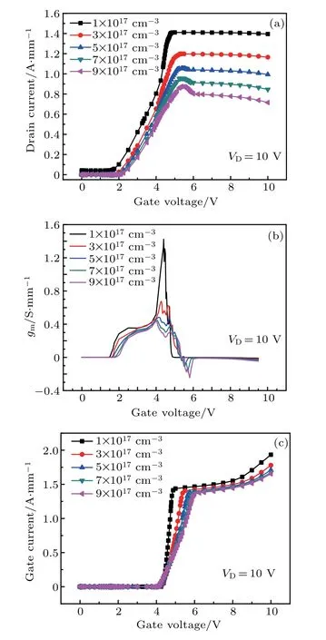
As earlier paper reported,trap concentration in UID GaN buffer can be higher than 1×1017cm−3when the UID GaN buffer layer was grown by MOCVD at lower growth rate.[26]To characterize the effect of trap concentration in the UID GaN buffer layer on the negative transconductance of the devices,five trap concentrations are selected to be 1×1017cm−3,3×1017cm−3,5×1017cm−3,7×1017cm−3,and 9×1017cm−3.The capture cross section is set to be 1×10⁻¹⁵cm2in this case.Figure 2 shows the VG–IDcurves of the devices with the five trap concentrations,where VDis 10 V,and VGis scanned from 0 V to 10 V in steps of 0.5 V.The threshold voltage of the devices is about 1.8 V.Normally,the drain current of the devices increases with the increase of gate voltage,and then is saturated when the gate voltage is large enough as indicated by the black and red curves in Fig.2.However,as we can see in Fig.2,the drain current drops when gate voltage is higher than 5 V and simultaneously the trap concentration reaches 5×1017cm−3,leading to a negative transconductance phenomenon.Therefore,concentration of traps in the UID GaN buffer layer is associated with negative transconductance of p-GaN gate AlGaN/GaN HEMTs.

Fig.2. (a)Transfer characteristics,(b)transconductance,and(c)IG–VG curves of devices,whereas trap concentrations are 1×1017 cm−3,3×1017 cm−3,5×1017 cm−3,7×1017 cm−3,and 9×1017 cm−3,and VD is 10 V.
Figure 3 shows the transfer characteristics of the devices with four capture cross sections,which are set to be 1×10⁻¹⁶cm2,1×10−15cm2,1×10−14cm2,and 1×10⁻¹³cm2,[24]where VDis 10 V,and VGis scanned from 0 V to 10 V in steps of 0.5 V.We set the trap concentration to be 3×1017cm−3in this case.As shown in Fig.3,the threshold voltage is about 1.8 V.When the capture cross section reaches 1×10⁻¹⁴cm2,the drain current drops at a gate voltage of about 5 V,leading to the negative device transconductance.Therefore,the capture cross section is also associated with the negative transconductance of the p-GaN gate AlGaN/GaN HEMT.

Fig.3. (a)Transfer characteristics,(b)transconductance,and(c)IG–VG curves of the devices,whereas trap capture cross sections are 1×10⁻¹⁶ cm2,1×10−15 cm2,1×10−14 cm2,and 1×10⁻¹³ cm2,and VD is 10 V.
3.Results and discussion
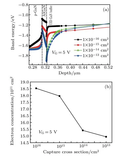
Traps in the UID GaN buffer layer are assumed to be acceptor-type traps which are unionized at zero gate bias,and they can ionize and capture electrons,with gate bias applied.This will influence the density and mobility of electrons in the channel,and hence influence drain current of device.In addition,electrons tunneling through the thin AlGaN barrier layer at a large gate bias can also influence the drain current.Drop in drain current at the large gate voltage means the occurrence of a negative transconductance phenomenon.In order to analyze the negative transconductance phenomenon associated with trap concentrations and capture cross sections as shown in Figs.2 and 3,we provide the band diagrams,output characteristics of the device,and electric field distribution.Figure 4 shows the conduction band diagrams of the devices with the five trap concentrations at a gate voltage of 5 V.The device is open at this status and electrons are collected in the AlGaN/GaN interface.Triangle barrier forms at AlGaN layer,and electrons have possibility to tunnel through the AlGaN layer.As shown in Fig.4(a),the triangle barrier becomes thinner with the increase of trap concentration,which makes it easier for the electrons in the potential well to tunnel through the AlGaN layer.These electrons can be attracted to the gate side and thus cause the gate current to increase as shown in Fig.2(c).As a result,the electron density in the channel decreases with trap concentration increasing as shown in Fig.4(b),and then results in a reduced drain current.Therefore,when trap concentration comes to a certain value,the negative transconductance phenomenon occurs.

Fig.4.(a)Band diagrams with five different trap concentrations.(b)Electron concentrations in channel.Gate voltage is set to be 5 V.
Figure 5(a)shows the output characteristics of the devices with the five different trap concentrations,with VGbeing 5 V,and VDbeing scanned from 0 V to 35 V.Because tunnel effect can influence the density of electrons in the channel as shown in Fig.4,the drain current in the saturation region increases with the decrease of trap concentration. Figure 5(b)shows the variations of Ronvalue with trap concentration of the device calculated in the linear region of ID–VDcurve for the five different trap concentrations,and we can see that the Ronincreases with the increase of the trap concentration.

Fig.5.(a)Output characteristics of devices with five different trap concentrations when VG=5 V.(b)Variations of Ron with trap concentration of devices with five trap concentrations calculated from curves in panel(a).

Fig.6.(a)Band diagrams with the four different trap cross sections.(b)Electron concentrations in channel,with gate voltage being set to be 5 V.
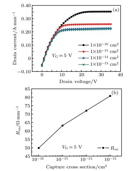
Similarly,figure 6(a)shows the conduction band diagrams of the devices with the four capture cross sections at a gate voltage of 5 V.It can be seen that the triangle barrier becomes thinner with the increase of the capture cross section and makes the tunnel process of electrons take place easier,which will reduce electron concentration in the channel as shown in Fig.6(b).These electrons can be attracted to the gate side and cause the gate current to increase as shown in the Fig.3(c).The calculated output characteristics of the devices show that the saturation current decreases with the increase of capture cross section as shown in Fig.7(a).The Ronvalues of the devices,calculated from linear region of Id–Vdcurve,increases with the increase of the capture cross section as shown in Fig.7(b).

Fig.7.(a)Output characteristics and(b)Ron of devices with different capture cross sections at VG=5 V.
The negative transconductance effect in the device can be attributed to the tunnel effect,which is related to the trap concentration and cross section in the UID GaN buffer layer as shown in Fig.8.The tunneling is Fowler–Nordheim(FN)tunneling,and the tunneling probability can be expressed as[27]

where m is the electron mass,φFis the barrier height from EF,d is the barrier width,and Ezis energy component of electrons normal to the barrier surface.The eVbiasis shown in Fig.8.The value of eVbiasincreases with trap concentration and trap cross section increasing as shown in Figs.4(a)and 6(a),which results in a larger TFN.And hence the electron concentration in the channel becomes smaller.Therefore,drain current drops at higher trap concentration and cross section.

Fig.8. Schematic diagram of tunnel effect resulting in negative transconductance.
Figure 9(a)shows the variations of electric field strength with gate voltageith at drain and gate side of the channel of the device with a trap concentration of 3×1017cm−3under different gate voltages. The values of VGare set to be 5,7,and 9 V,because the negative transconductance appears when VGreaches 5 V as shown in Fig.2.We can see from Fig.9(a)that the value of electric field at drain side is higher than that at gate side with the increase of the gate voltage,but the difference between them decreases at higher gate voltage.Figure 9(b)shows the difference in electric field between drain side and gate side for the five trap concentrations,where VGis 7 V.The difference in electric field between drain side and gate side decreases with trap concentration increasing. This decrease causes the difference in electron mobility between drain side and gate side to increase. Therefore,more carriers are attracted to the gate side with larger trap concentration,which leads the drain current to decrease.As a result,the reduced drain current at large trap concentration will cause a negative device transconductance as shown in Fig.2.

Fig.9.Electric field strength at drain and gate sides of the channel of the device with(a)trap concentrations of 3×1017 cm−3 and(c)capture cross section of 1×10⁻¹⁵ cm2 under different gate voltages.Difference in electric field between drain side and gate side for(b)five different trap concentrations and(d)four capture cross sections,with VG being 7 V.

Fig.10.Mechanism of negative transconductance,with VG>5 V.
Similarly,the difference in electron mobility between drain side and gate side decreases with capture cross section increasing,which leads the drain current to decrease,which finally gives rise to the negative transconductance effect.
In conclusion,when gate voltage reaches 5 V,more electrons are attracted to the gate side at higher trap concentration and capture cross section,which results in a decrease of drain current and an increase of gate current as shown in Fig.10.
4.Conclusions
In this paper we study the negative transconductance effect in p-GaN gate AlGaN/GaN HEMTs that is associated with traps in the unintentionally doped GaN buffer layer.By simulation,we find that electrons are easier to tunnel through Al-GaN barrier layer with increasing trap concentration and capture cross section,and simultaneously,the difference of electric field between drain side and gate side decreases. As a result,drain current drops and hence results in the occurrence of negative transconductance effect.This phenomenon occurs when the trap concentration reaches 5×1017cm−3(whereas capture cross section is 1×10⁻¹⁵cm2)and capture cross section reaches 1×10⁻¹⁴cm2(whereas trap concentration is 3×1017cm−3).
Acknowledgment
The authors thank colleagues of Prof. Chen Dunjun’s group for their help.
- Chinese Physics B的其它文章
- Theoretical analyses of stock correlations affected by subprime crisis and total assets:Network properties and corresponding physical mechanisms∗
- Influence of matrigel on the shape and dynamics of cancer cells
- Benefit community promotes evolution of cooperation in prisoners’dilemma game∗
- Theory and method of dual-energy x-ray grating phase-contrast imaging∗
- Quantitative heterogeneity and subgroup classification based on motility of breast cancer cells∗
- Designing of spin filter devices based on zigzag zinc oxide nanoribbon modified by edge defect∗

