
Direct deposition of graphene nanowalls on ceramic powders for the fabrication of a ceramic matrix composite∗
2019-06-18 05:42HaiTaoZhou周海涛DaBoLiu刘大博FeiLuo罗飞YeTian田野DongShengChen陈冬生BingWeiLuo罗炳威ZhangZhou周璋andChengMinShen申承民
Chinese Physics B 2019年6期
Hai-Tao Zhou(周海涛),Da-Bo Liu(刘大博),Fei Luo(罗飞),Ye Tian(田野),Dong-Sheng Chen(陈冬生),Bing-Wei Luo(罗炳威),†,Zhang Zhou(周璋),and Cheng-Min Shen(申承民),‡
1Beijing Institute of Aeronautical Materials,Aero Engine Corporation of China,Beijing 100095,China
2Beijing National Laboratory of Condensed Matter Physics,Institute of Physics,Chinese Academy of Sciences,Beijing 100190,China
Keywords:graphene,ceramic matrix composite,chemical vapor deposition
1.Introduction
Monolithic ceramics are widely used in the materials industry,including wear-resistance parts,electronics,and various coatings. However,their applications are significantly limited by the brittleness and poor electrical conductance.To overcome these drawbacks,ceramic composites have been developed by incorporating nano fillers into the ceramic matrices.[1-6]Recently,graphene has been widely investigated as a good filler for producing highly tough and stiff ceramic matrix composite(CMC).[7-15]According to the papers reported in this field,the main challenges have been to produce high quality graphene and realize good dispersion of graphene in ceramic matrix.In these studies,ball-milling[7-12]and colloidal processing[13-15]were two mainly used mixing methods.Ball-milling technique imposed heavy shear forces on graphene to break its agglomeration and promote its dispersion.Colloidal processing produced well dispersed mixture usually by adding graphene oxide(GO)dropwise into ceramic suspension under magnetic stirring.However,the severe collision in ball-milling and the oxidation treatment in preparing GO by hummer’s method would all significantly damage the graphene flakes and give rise to massive structural defects,[16,17]which degraded the physical properties in contrast with pure graphene.To produce high quality CMC,it is necessary to develop a new method to realize better control of the quality of graphene,as well as uniform mixing.
Recent years have witnessed great progress in the growth of graphene nano walls(GNWs)on arbitrary substratesby employing plasma-enhanced chemical vapor deposition(PECVD)(PECVD)technique.[18-23]This method enables the lowtemperature and uniform synthesis of graphene nanosheets owing to the presence of reactive species generated in the plasma region,and the GNWs have been widely used in the aspects of solar cells,supercapacitor,and field emission.[19,20,22]In this study,we aim to utilize PECVD to directly deposit graphene on the surface of ceramic powder,and the morphology and theinitial stage ofgrowth process of GNWshave been investigated.
2.Experimental procedure
2.1.Growth of GNWs on the ceramic powder
The α-alumina powder(Xilong Scientific Ltd.)with a purity of 99.85%and an average particle size of 50µm was studied.GNWs were deposited in a remote radio-frequency(RF)PECVD system.Thin powder layer was flatly laid in the bottom of the crucible and then transferred into the quartz tube furnace.Prior to deposition,the furnace was pumped down to a pressure of 5×10⁻¹Pa,then the temperature was raised to 600°C or 700°C at a rate of 20°C/min under the protection of Ar flow of 150 standard cubic centimeters per minute(sccm).Thereafter,CH4flow(20 sccm)was introduced into the furnace and 290 W RF was generated simultaneously.After the deposition,the RF and CH4flow were turned off and the ceramic powder was naturally cooled down to room temperature.
2.2.Spark plasma sintering(SPS)
Bulk ceramic composite was fabricated using an SPS-1050 T apparatus.The powder was loaded in a cylindrical graphite die with an inner diameter of 40 mm.Two graphite plungers were used to seal the die on both ends.The sintering process was carried out under a vacuum of 5 Pa and a uniaxial pressure of 4 MPa was applied.Samples were heated to 1450°C at a rate of 10°C/min.The dwelling time was 5 minutes.
2.3.Characterizations
The microstructure of the powder was characterized by scanningelectronmicroscope(SEM,HitachiS-4800)andhigh resolution transmission electron microscope(HRTEM,FEI Tecai G2F20).Raman spectrum was recorded on the Horiba Jobin Yvon LabRAM HR-800 with a laser wavelength of 532 nm and an incident power of 1 mW.The x-ray photoelectron spectroscopy(XPS)analysis was carried out on Thermo escalab 250XI,using monochromatized Al Kα radiation at 150 W.The high resolution XPS spectra were recorded in the constant analyzer energy(CAE)mode with a pass energy of 20 eV and a step size of 0.1 eV.The density values were measured using the Archimedes method.Vecker hardness tests were carried out on the Future-Tech with a 100-g force.Keysight 2902A was used to measure the conductivity at 25°C on a small piece of sample with a size of 8 mm×8 mm×0.5 mm.
3.Results and discussion
Figure 1(a)shows a schematic illustration of the remote PECVD system,in which the RF helical-coil is mounted at the upstream side and could dissociate the methane gas into various active radicals.Owing to these radicals,the growth of GNWs does not depend on the catalytic decomposition of the precursor by the metallic substrate and could be realized on almost arbitrary substrates from metal to insulator,such as copper,silicon,andglass.[22,24,25]Figure1(b)showsacomparison photograph,from which we could clearly find that the alumina(Al2O3)powder completely turns black after the GNWs deposition of 90 min.Raman spectrum in Fig.1(c)veri fies the formation of GNWs and presents three intrinsic peaks located at 1353 cm-1,1590 cm-1,and 2697 cm-1,corresponding to D band,G band,and 2D band of grapheme,respectively.[26,27]XPS analysis is used to study the chemical composition of the GNWs.Figure 1(d)is a representative spectrum,showing a strongC1speakat284.8eVandasmallO1speakat532.5eV.No other elements are detected in the GNWs except for some oxygen adsorbates.The existence of these oxygen adsorbates is due to the physical and/or chemical adsorption of oxygen when the sample is exposed to ambient conditions.
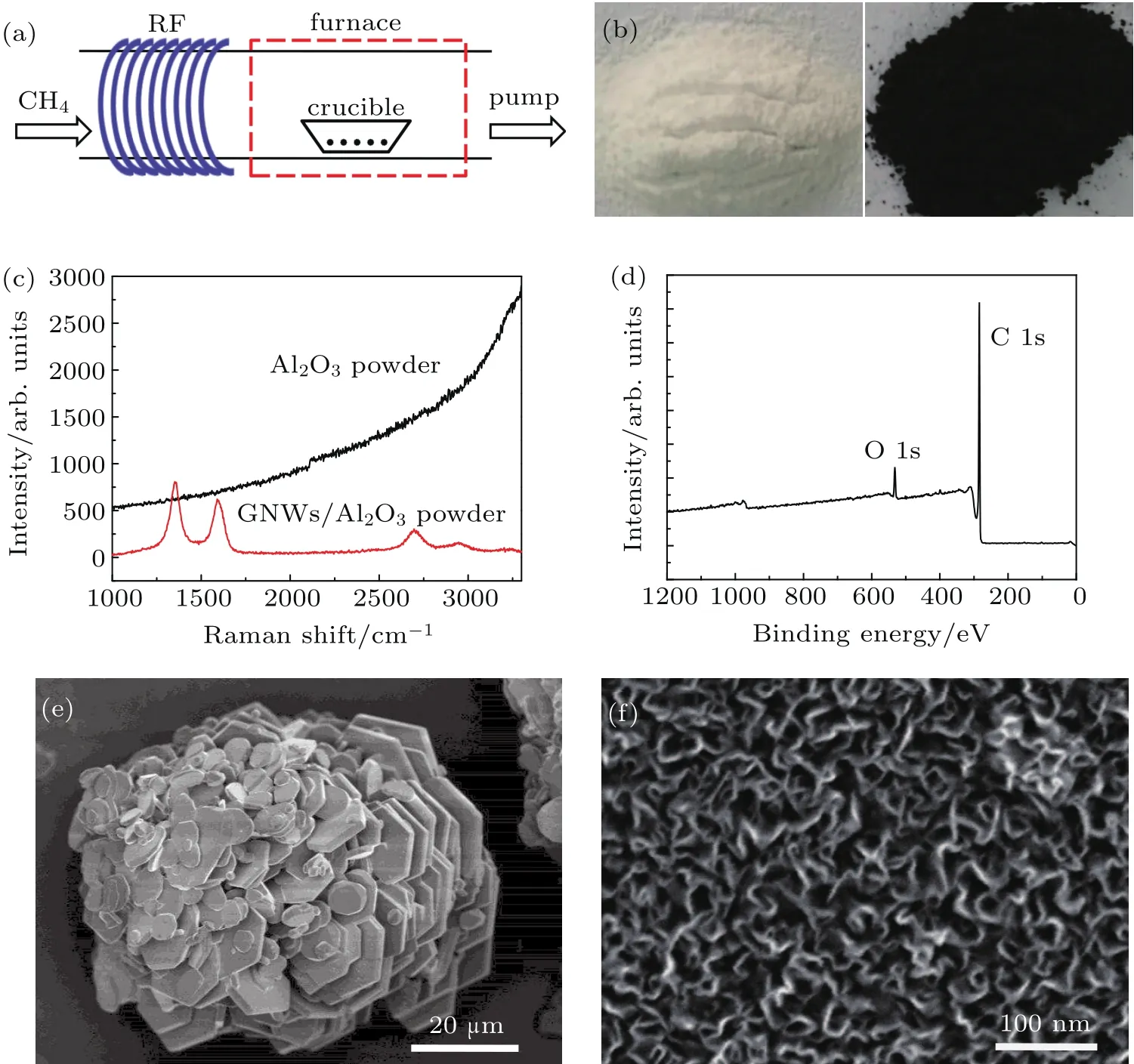
Fig.1.(a)Schematic illustration of PECVD system.(b)Photographs of Al2O3powder before(left)and after(right)GNWs deposition.(c)Raman spectrum.(d)XPS of GNWs/Al2O3powder.(e)Low-magni fication SEM image showing overall view of Al2O3particles.(f)High-magni fication image showing GNWs on the particle.Graphene deposition parameter:700°C,290 W,90 min.
The large-scale SEM image in Fig.1(e)is an overall view of a single alumina particle.The particle has a size of∼50µm and consists of numerous alumina pieces.The morphology and structure of the GNWs-capping on the alumina particle are analyzed by the SEM and HRTEM techniques.From the higher-magni fication SEM image(Fig.1(f)),GNWs could be clearly identi fied,showing a curled-sheet feature and an average length of∼70 nm.According to the previous report,GNWs are composed of two kinds of structures,named stem-and branch-structures.[23]The graphene sheets visible in Fig.1(f)are referred to as stem.As shown in Fig.2(a),we could see the branches at much higher magni fication,in which several stem-and branch-structures are labeled by the solid and dashed arrows,respectively.The branches are much smaller and dimmer compared with the stems.To further understand the structure of GNWs,TEM is harnessed to study the morphology.Figure 2(b)shows a typical TEM image of a single sheet of GNWs.Dense branches with the size of several nanometers could be clearly identi fied,and three of them are labeled by arrows to guide the eye.HRTEM images could be used to identify the graphene layers.The image(Fig.2(c))obtained at the edge of stem-structure indicates that this stem is terminated with two-layer graphene.The interlayer spacing between two neighboring monolayer is about 0.37 nm.This value is slightly larger than that of graphite,which is most likely due to the reduced interactions between graphene layers.[19]Figure 2(d)shows an HRTEM image recorded in the zone of branches,from which we could find that the branches are composed of various graphene layers with an average interlayer spacing of 0.374 nm.These results imply that the GNWs films correspond to few-layer graphene.
Many efforts have been made to investigate the growth mechanism of GNWs on metallic substrates,such as Cu,Ni,and Pt.[22,23,28]Most of these studies indicated that the growth of GNWs was composed of two stages:initially,the carbon radicals nucleated and massive graphene layers in parallel with substrate took form,following a two-dimensional(2D)growth mode;as the number of layers increased and the strain energyaccumulated, 2D layers became energetically unfavorable and a transition to three-dimensional(3D)growth took place.However,However, few work reported the growth mechanism on the surface of ceramics.To elucidate this issue,the growth process of GNWs is monitored by gradually varying the growth time under otherwise the same condition.Before graphene deposition,the surface of alumina particle has a clean and smooth topography,as shown in the SEM image of Fig.3(a).After 10 min deposition(Fig.3(b)),graphene sheets with wrinkle structures could be clearly identi fied.At this stage,these sheets are still lying down on the substrate.When the deposition time is elongated to 20 min(Fig.3(c)),the transition to 3D growth occurs and some graphene sheets stand up at the substrate,as labeled by solid arrows.The above observations prove that the growth of GNWs on ceramic surface also complies well with the two-stage mode.According to this mode,we could control the lateral width of the graphene sheets by changing the growth temperature.[22]As shown in Figs.3(d)and 3(e),at a growth temperature of 700°C,all the sheets of GNWs present similar width of 70 nm;in contrast,the width increases to 150 nm at 600°C.In ball-milling and colloidal methods,the size of graphene flakes is incontrollable.Thus,no work so far has reported the effect of the size distribution of graphene sheets on the properties of CMC.In our experiment,the size of graphene sheets is uniform at a given growth temperature and is adjustable by changing the temperature,which makes the study of size effect feasible.
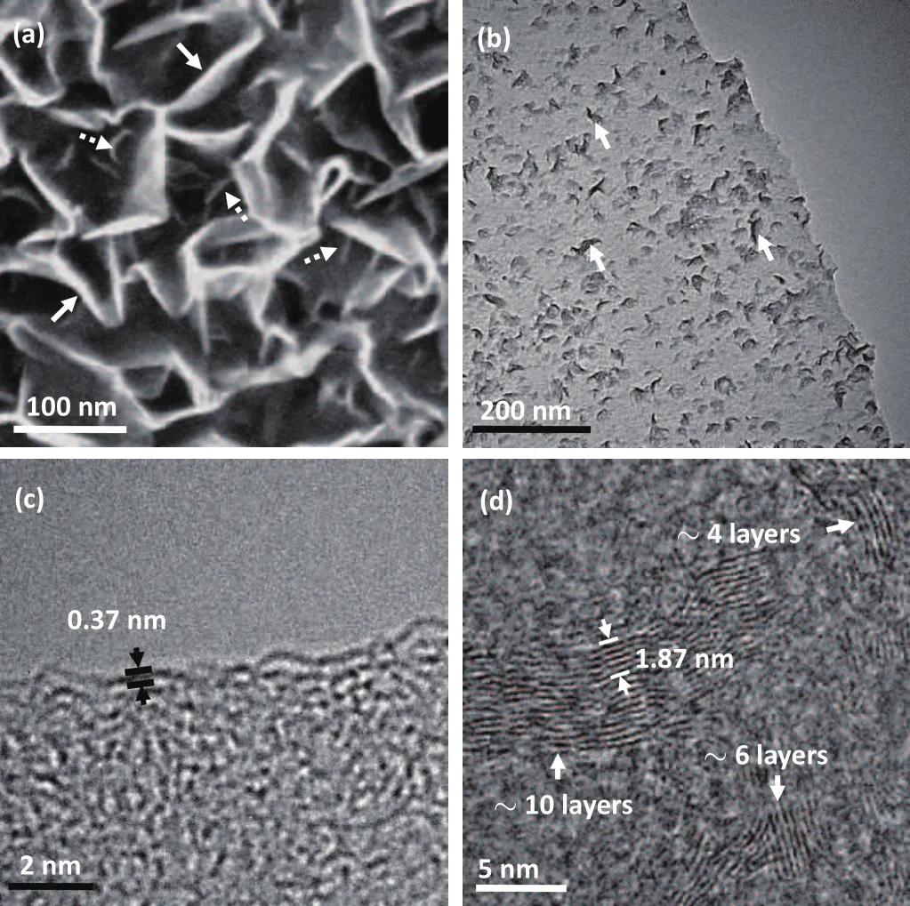
Fig.2.(a)High-magni fication SEM image showing abundant of stem-(solid arrows)and branch-(dashed arrows)structures.(b)TEM image of branches(labeled by arrows)on the stem.(c)HRTEM image at the edge of the stem,indicating the stem is terminated with two-layer graphene with an interlayer spacingof0.37nm.(d)HRTEMimageatthebranches,showingthebranches are composed of various graphene layers with an average interlayer spacing of 1.87/5=0.374 nm.
XPS measurements are also carried out to detect the growth process of GNWs.Before deposition,the bare Al2O3powder is treated at ambient atmosphere at 800°C for three hours. Our results indicate that the content of residual amorphous carbon significantly decreases from 12.3 at.%to 7.1 at.%after this treatment.The high-resolution C 1s spectra recorded at different deposition times are presented in Fig.3(f).The amorphous carbon on bare Al2O3powder shows a broad C 1s peak and a maximum at 284.68 eV.The peak recorded after 1-min deposition is obviously different,which is located at 284.79 eV and shows a characteristic shape of C 1s spectrum of graphitic carbon.This peak could be fitted with two peaks at 284.8 eV and 285.5 eV,corresponding to graphitic carbon and C-O bond,respectively.The existence of C-O bond might be due to the fact that the carbon radicals partially reduce the Al2O3surface and the Al-O-C bonds form.[29]There is almost no change in the shape of C 1s when the deposition time is elongated to 3 min.The carbon concentrations measured on the powder surface are 34 at.%and 48 at.%after 1-min and 3-min depositions,respectively.
To elucidate the universality and advantage of our method,we further deposit GNWs on the surface of silicon nitride(Si3N4).As shown in the SEM image of Fig.4(a),the Si3N4powder shows a particle size of below 3µm.At higher magni fication,graphene sheets could be identi fied with an average length of 70 nm and 150 nm at the growth temperature of 700°C(Fig.4(b))and 600°C(Fig.4(c)),respectively.The Raman spectrum in Fig.4(d)presents three peaks located at 1350 cm-1(D),1586 cm-1(G),and 2702 cm-1(2D),further verifying the formation of GNWs.The results are similar to these on alumina powder,indicating that the growth of GNWs is independent on the type of ceramic powder and could be further extended to other powders such as SiC,SiO2,and mullite.

Fig.4.(a)Low-magni fication SEM image showing overall view of Si3N4 particles.(b)and(c)High-magni fication image of GNWs on the particle,showing variable lateral lengths at different growth temperatures.(d)Raman spectrum.Graphene deposition parameters are:(b)700°C,290 W,90 min;(c)600°C,290 W,90 min.
The GNWs-Al2O3powder is sintered by SPS method to fabricate alumina composite.The volume percent of graphene in this sample is about 0.25%.Pure Al2O3powder is also sintered to bulk monilithic alumina using the same condition for comparison.The composite has a black color,exhibiting a sharp contrast with the white monolithic alumina.Graphene owns exceptional high electrical conductivity and is considered to be an ideal additive to improve this property of ceramic.[7,16,30]We carry out measurements on several physical properties such as bulk density,Vickers hardness,and electrical conductivity.The monilithic alumina and the composite exhibit similar bulk density with the value of 3.899 g/cm3and 3.918 g/cm3,respectively.These numbers are very close to the ideal value of alumina(3.97 g/cm3),indicating that the sintering parameters used in our experiment are suitable.There are little differences in hardness between the two samples,with the value of 1667 HV and 1652 HV,respectively.However,the addition of graphene could significantly raise the electrical conductivity of alumina.Our experiment results show that the monilithic Al2O3is an insulator.The graphene sheets in the composite provide numerous conductive paths and sharply increase the electrical conductivity to a value of 0.724 S/m.
4.Conclusion and perspectives
GNWs film has been successfully deposited on the surface of Al2O3and Si3N4powders.The layers,counted from HRTEM images,imply that the GNWs correspond to fewlayer graphene.SEM results indicate that the growth process includes a transition from 2D to 3D mode at the initial stage.The lateral length of graphene sheets could be well controlled by changing the deposition temperature,which is about 70 nm and 150 nm at 700°C and 600°C,respectively.Moreover,the electrical conductivity of the composite significantly increases compared with the monilithic alumina.Our experiment provides an alternative way to realize the uniform mixing of graphene and ceramic powders,which has potential applications in fabricating ceramic matrix composites.
猜你喜欢
学与玩(2022年10期)2022-11-23
小猕猴智力画刊(2022年10期)2022-11-02
国画家(2022年3期)2022-06-16
人大建设(2020年1期)2020-07-27
金桥(2018年5期)2018-09-22
黄河之声(2016年12期)2016-11-07
中国火炬(2015年11期)2015-07-31
幼儿时代·故事妈妈(2004年3期)2004-03-17

- Chinese Physics B的其它文章
- Topological superconductivity in a Bi2Te3/NbSe2heterostructure:A review∗
- The universal characteristic water content of aqueous solutions∗
- Neutral excitation and bulk gap of fractional quantum Hall liquids in disk geometry∗
- Hard carbons derived from pine nut shells as anode materials for Na-ion batteries∗
- Crystal structures and sign reversal Hall resistivities in iron-based superconductors Lix(C3H10N2)0.32FeSe(0.15<x<0.4)∗
- Improved electrochemical performance of Li(Ni0.6Co0.2Mn0.2)O2 at high charging cut-off voltage with Li1.4Al0.4Ti1.6(PO4)3 surface coating∗