LNA Design for Future S Band Satellite Navigation and 4G LTE Applications
Muhammad Arsalan and Falin Wu,
Abstract: A good design of LNA for S band satellite navigation receivers and 4G LTE wireless communication system has been implemented in this paper.Due to increased congestion in the present L band, the S Band frequency from 2483.5-2500 MHz has been allocated for the future satellite navigation systems.For this purpose ATF-34143 amplifier (pHEMT) having high electron mobility and fast switching response has been chosen due to its very low Noise Figure (NF).The amplifier has been designed having bandwidth of 0.8 GHz from 1.8-2.6 GHz.Because of the large bandwidth, the amplifier could serve many wireless communication applications including 4G LTE mobile communication at 2.1 GHz.The design was implemented using the micro strip technology offering extremely low noise figure of 0.312 dB and 0.377 dB for 2.1 GHz and 2.49 GHz respectively.The gain of the amplifier was low and found to be 10.281 dB and 9.175 dB.For the purpose of increasing the gain of an amplifier, the proposed LNA design was then optimized by using Wilkinson Power Divider (WPD).The Balanced LNA design using WPD offered very low noise figure of 0.422 dB and 0.532 dB respectively and the gain was considerably increased and was found to be 20.087 dB and 17.832 dB respectively against 2.1 GHz and 2.49 GHz.Simulations and measurements were taken in Agilent Advanced Design System (ADS) software.The suggested LNA can be used for a variety of wireless communications applications including the future S band satellite navigation systems.
Keywords: Long term evolution, low noise amplifier, wireless communication, satellite navigation, global navigation satellite system, wilkinson power divider.
1 Introduction
Presently the Global Navigation Satellite System (GNSS) technology has grown rapidly all around the world and many countries are trying their best to use their own navigation satellite systems to cope up.Because of this, the Radio Frequency (RF) band which is currently allocated for GNSS is not adequate for providing several planned services for the future due to congestion in the current spectrum especially in E1 and L1 bands [Liu, Liang, Morton et al.(2014); Betz (2013)].Consequently, there is a need for a new frequency band to be used for the s atellite navigation systems in addition to L Band [Svaton (2015)].Thus, the S Band frequency from 2483.5-2500 MHz of RF spectrum has been allocated for future satellite navigation systems [Sun, Xue, Zhao et al.(2017); Xue, Sun and Zhao (2015)].
The low noise amplifier is the first stage of the receiver chain and is considered to be very important because of its noise characteristics [Arsalan and Wu (2018)].The RF signal which is received by the antenna needs to be amplified because it is of weak strength and then it can be demodulated.So, the noise figure of LNA should be extremely low otherwise the noise along with the received signal might get amplified.In recent years the design of low noise amplifier having wide bandwidth is a difficult task because as the conjugate matching will provide good gain only for narrow bandwidth.There is a compromise between the Noise Figure (NF), Gain, impedance matching, stability and linearity on the performance of the device and so it becomes bit challenging for the designer to design a high performance optimized LNA for proposed applications.The main aim of this research is to propose an optimized low noise amplifier design offering very low noise figure of less than 0.6 dB and with an appreciable amplifier gain so that it can be utilized in the receiver chain of radio frequency front-end.The finalized Balanced LNA design gives extremely low noise figure of 0.422 dB and 0.532 dB respectively and the gain was found to be considerably good measuring 20.087 dB and 17.832 dB respectively against 2.1 GHz and 2.49 GHz.The designed LNA can be used for a diverse nature of applications such as wireless, mobile communications and future S band satellite navigation systems.
The paper layout is given as: in Section 2 active device is decided.Analyzing stability of single stage LNA is shown in Section 3.In Section 4 the design techniques and analysis of single stage LNA with micro strip element design are presented.Stability analysis of Balanced LNA is shown in Section 5.The wide bandwidth response of LNA by using Wilkinson power divider with the simulation results are presented in Section 6.Section 7 covers the conclusion of this paper.
2 Active device selection for amplifier design
In this case the LNA has to be designed which can offer very low noise figure (<0.6 dB) with substantial gain, the selection of suitable active device is of high importance.If you choose the wrong active device then the optimized design cannot fulfill the design requirements of LNA for the proposed applications.
Initially the comparison of different amplifier ICs used for L band and S band LNA design.There should be careful look at the noise figure, gain and power consumption of the amplifier.Since the aim of this research is to propose an LNA with minimum achievable noise figure of <0.6 dB, the Avago Technology ATF-34143 device was chosen for the design of LNA because a quick response and high mobility is achieved in HEMT devices [Sze and Ng (2006)].
The proposed LNA will be used in the receiver circuitry so it must offer minimum noise figure showing the efficiency and resulting in the better performance of the system.
3 Stability analysis of single stage amplifier
For any specified application, the LNA must not become unstable during the given frequency band.
Some oscillations might occur due to source and load terminations which will affect the impedances at the input side as well as at the output side of the device.To avoid the instability of the device, the reflection coefficients must reside inside the stable area of the smith chart.The reflection coefficients at the input and output side of transistor can be defined in mathematical form as

where Γinand Γoutare input and output reflection coefficients respectively, S11, S12, S21and S22are input return loss, reverse transmission coefficient, forward transmission coefficient and output return loss respectively.Mathematically, the Rollett criterion (k) can check for the stability for which the value of k>1 signifies unconditional stability and vice versa [Arsalan, Amir and Khan (2014); Pozar (2001); Gonzalez (1997)].

where, Δ=S11S22- S12S21.
The device stability plot based on the Rollett’s Stability criterion (K) is shown in Fig.1.Stability of the device can also be tested from mu source and load as shown in Fig.2.
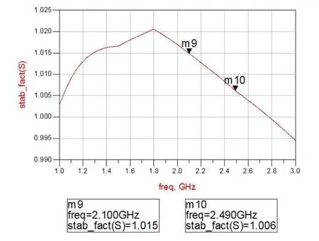
Figure 1: Device stability plot
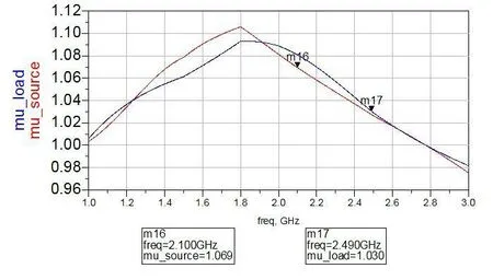
Figure 2: Device stability in terms mu source or mu load
4 Design techniques and analysis of single stage amplifier
In the design techniques, impedances must be matched at the input and output side of the device for stable design and maximum power transfer.Good matching of the device can be seen by observing the values of input and output reflection coefficients on the smith chart or in dB scale.If their values are below 10 dB or their values are closely approaching to the nominal 50 ohms on the smith chart, the matching of the device is good enough.The input and output reflection coefficients on the dB scale are shown in Figs.3 and 4 respectively and those on the smith chart are shown in Figs.5 and 6 respectively.
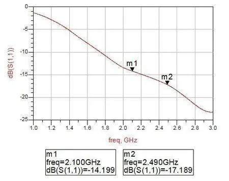
Figure 3: S11 of a matched transistor
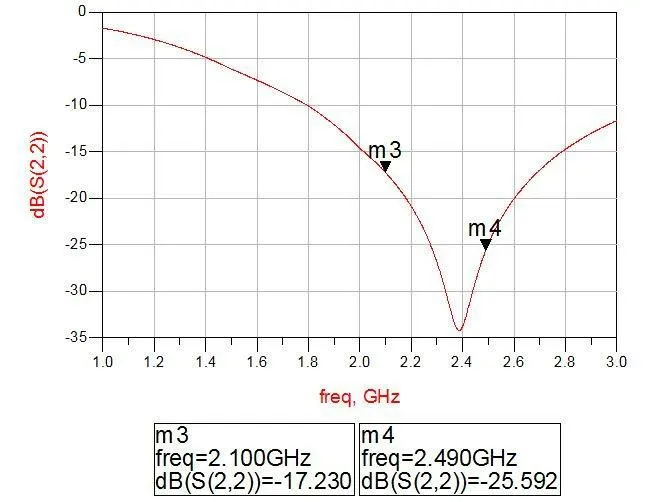
Figure 4: S22 of a matched transistor
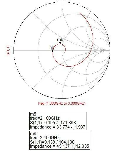
Figure 5: S11 of matched transistor on smith chart
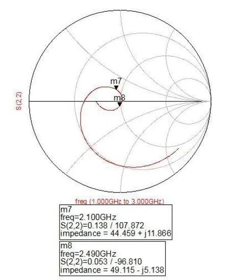
Figure 6: S22 of matched transistor on smith chart
The values are below 10 dB on the dB scale that is for input reflection coefficient the value is -17.189 dB and for the output reflection coefficient the value is -25.592 dB which shows good matching of the amplifier.
The noise figure of finalized single stage LNA is found to be extremely low and measured to be 0.312 dB and 0.377 dB respectively and the gain of the amplifier is found to be 10.281 dB and 9.175 dB respectively for 2.1 GHz and 2.49 GHz respectively as shown in Figs.7 and 8.The values of reverse transmission coefficient of the LNA are also below 10 dB which are acceptable as shown in Fig.9.
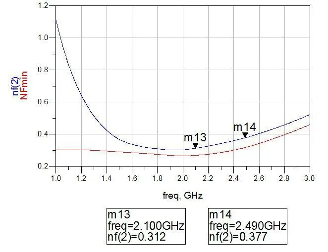
Figure 7: Noise figure of single stage LNA
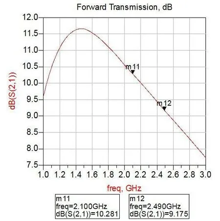
Figure 8: Gain of single stage LNA
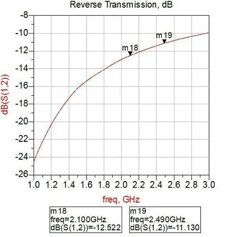
Figure 9: Reverse transmission coefficient of single stage LNA
5 Stability analysis of balanced amplifier
Simulation results show that the balanced LNA is unconditionally stable throughout the opted frequency band that is from 1.8-2.6 GHz.The value of (k) is also found to be greater than one as well as the values of mu source and load are also found to be greater than one as shown in Figs.10 and 11 respectively.
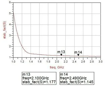
Figure 10: Stability plot of balanced LNA
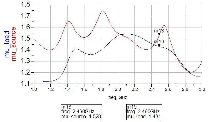
Figure 11: Stability of balanced LNA in terms mu source or load
6 Design techniques and analysis of balanced amplifier
Similarly balanced configuration of low noise amplifier has been designed by using Wilkinson power divider.Simulation results show that the values of input and output reflection coefficient are below 10 dB scale as shown in Figs.12 and 13 respectively.
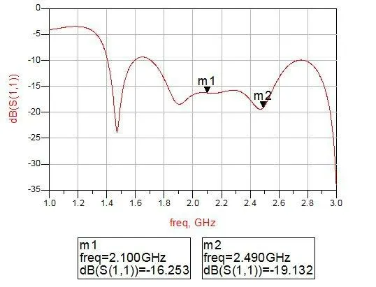
Figure 12: Input reflection coefficient of balanced LNA
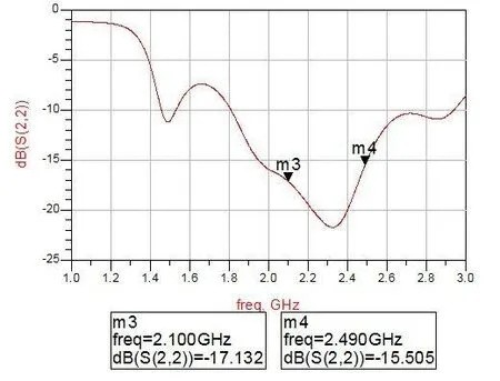
Figure 13: Output reflection coefficient of balanced LNA
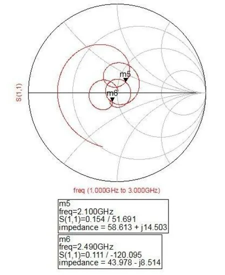
Figure 14: S11 of balanced LNA
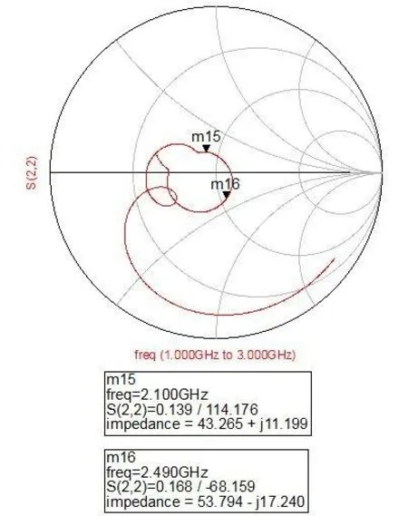
Figure 15: S22 of balanced LNA
The values of reflection coefficients at the input side and output side of the amplifier are measured to be -19.132 dB and -15.505 dB respectively which are below 10 dB scale.Likewise their plot on the smith chart are about to approach nominal 50 ohms indicating good matching of the transistor as shown in Figs.14 and 15 respectively.
The noise figure of Balanced LNA is found to be 0.422 dB and 0.532 dB for 2.1 GHz and 2.49 GHz respectively which is very low and so this LNA will serve as a very good candidate in the receiver chain.Also, the gain of Balanced LNA is measured to be 20.087 dB and 17.832 dB respectively for 2.1 GHz and 2.49 GHz respectively which is considered to be significant.
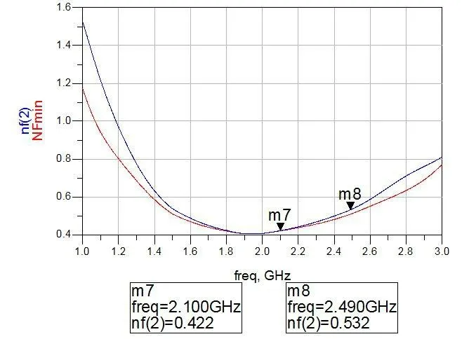
Figure 16: Noise figure of balanced LNA
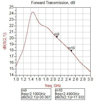
Figure 17: Gain of balanced LNA
The reverse transmission coefficient of the balanced LNA design are also measured to be significantly below 10 dB scale showing good matching and design of the amplifier as shown in Fig.18.
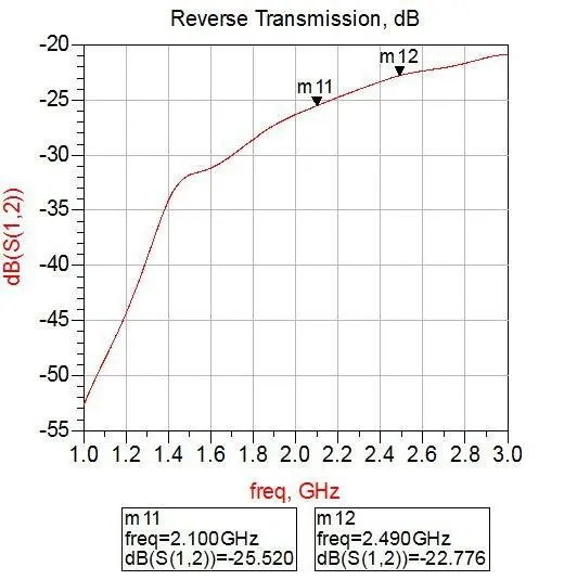
Figure 18: Reverse transmission coefficient of balanced LNA
Tab.2 shows the performance summary of single stage and Balanced LNA design.Different LNA working in the GNSS frequencies have been evaluated with the proposed LNA design as given in Tab.3.

Table 2: Performance summary of single stage and optimized balanced LNA design
7 Conclusions
In this paper, LNA has been designed, simulated and optimized for future S band satellite navigation receivers.Wide bandwidth of balanced LNA design makes it useful for vast variety of applications including wireless communication and 4G LTE mobile communication systems.The optimized balanced LNA design depicts extremely low noise figure of be 0.422 dB and 0.532 dB for 2.1 GHz and 2.49 GHz respectively.The gain of Balanced LNA is measured to be 20.087 dB and 17.832 dB respectively for 2.1 GHz and 2.49 GHz respectively which is significant for the first stage of RF frontend.
References
Arsalan, M.; Amir, F.; Khan, T.(2014): Phemt LNA design and characterization for 4G applications.17th IEEE International Multi Topic Conference.
Arsalan, M.; Wu, F.(2018): An S band tracking receiver LNA for satellite communications.International Workshop on Antenna Technology.
Betz, J.W.(2013): Signal structures for satellite-based navigation: past, present and future.Inside GNSS, vol.8, pp.34.
Chen, D.; Pan, W.; Jiang, P.; Jin, J.; Mo, T.et al.(2012): Reconfigurable dual-channel multiband RF receiver for GPS/Galileo/BD-2 systems.IEEE Transactions on Microwave Theory and Techniques, vol.60, no.11, pp.3491.
Dobeš, J.; Michal, J.; Popp, J.; Grabner, M.; Vejrazka, F.et al.(2015): Multiobjective optimization of a low-noise antenna amplifier for multi-constellation satellitenavigation receivers.28th IEEE International System-on-Chip Conference.
Fathima, A.; Sushma, P.; Gaonkar, S.(2016): Design of high gain low power CMOS multi-standard LNA.International Conference on Recent Trends in Electronics Information Communication Technology.
Gonzalez, G.(1997): Microwave Transistor Amplifiers Design and Analysis, 2nd ed.New Jersey: Prentice Hall.
Liu, X.; Liang, M.; Morton, Y.; Closas, P.; Zhang, T.et al.(2014): Performance evaluation of MSK and OFDM modulations for future GNSS signals.GPS Solutions, vol.18, no.2, pp.163-175.
Luo, Y.; Qian, M.; Gan, Y.; Ye, T.; Ma, C.(2015): Analysis and optimal design of SiGe HBT low noise amplifier for GNSS receiver.IEEE 16th International Conference on Communication Technology.
Lv, J.; Bao, Y.; Huang, J.(2016): Wideband low noise amplifier using a novel equalization.Progress in Electromagnetic Research Symposium.
Pozar, D.(2001): Microwave and RF Design of Wireless Systems, 3rd ed.John Wiley & Sons Inc.
Safari, M.; Eghtesadi, M.; Mosavi, M.R.(2016): A concurrent dual band low noise amplifier for GNSS receivers.Iranian Journal of Electrical and Electronic Engineering, vol.12, no.2, pp.119-125.
Sun, Y.; Xue, R.; Zhao, D.; Wang, D.(2017): Radio frequency compatibility evaluation of S band navigation signals for future BeiDou.Sensors, vol.17, no.5.
Svaton, J.(2015): Experimental reception of new GNSS signals.International Association of Institutes of Navigation World Congress.
Sze, S.; Ng, K.(2006): Physics of Semiconductor Devices.3rd ed.New York: Wiley-Blackwell.
Wang, S.(2014): A GaAs MMIC LNA design for wideband satellite communication receiver application.IEEE International Conference on Communication Problem-Solving.
Xue, R.; Sun, Y.; Zhao, D.(2015): CPM signals for satellite navigation in the S and C bands.Sensors, vol.15, no.6, pp.13184.
 Computer Modeling In Engineering&Sciences2019年5期
- Computer Modeling In Engineering&Sciences的其它文章
- The Quality Assessment of Non-Integer-Hour Data in GPS Broadcast Ephemerides and Its Impact on the Accuracy of Real-Time Kinematic Positioning Over the South China Sea
- RAIM Algorithm Based on Fuzzy Clustering Analysis
- Exploring Urban Population Forecasting and Spatial Distribution Modeling with Artificial Intelligence Technology
- Inferring Spatial Distribution Patterns in Web Maps for Land Cover Mapping
- Monitoring Multiple Cropping Index of Henan Province, China Based on MODIS-EVI Time Series Data and Savitzky-Golay Filtering Algorithm
- Frequency Domain Filtering SAR Interferometric Phase Noise Using the Amended Matrix Pencil Model
