Electronic Structures and Optical Properties of Ga Doped Single-Layer Indium Nitride
Zhi-wei Li,De-ping Guo,Gung-yi Hung,Wng-li To,Mn-yi Dun,b∗
a.College of Physics and Electronic Engineering,Sichuan Normal University,Chengdu 610101,China
b.Division of Interfacial Water and Key Laboratory of Interfacial Physics and Technology,Shanghai Institute of Applied Physics,Chinese Academy of Sciences,Shanghai 201800,China
I.INTRODUCTION
Since graphene was discovered by Novoselov et al.in 2004[1],many researchers have been attracted by the excellent electronic structure and optical properties of single-layer materials.Group-III nitrides,such as GaN,AlN and InN,have been explored for many years,and the InN material had been proved that it can be applied in making microelectronic and photoelectric devices[2−4],tunnel junctions[5],single photon emitters[6]and polarization-driven topological insulators[7],because it has the highest mobility[8],peak rate,electron drift rate[9,10],and the smallest effective electron mass[11].These discoveries open a new door to further explore the properties of InN materials.However,compared to three-dimensional materials,two-dimensional materials have more excellent physical and optical properties.Single-layer materials are more sensitive to external regulation and many researchers have predicted the potential applications in the fields of modern nanotechnologies[12−15].
In 2006,Kang et al.used metal organic chemical vapor deposition(MOCVD)technique to obtain high quality hexagonal symmetrical indium nitride nanoflower structure for the first time by means of hydrogeninduced“autocatalysis”[16,17].In 2009,Komissarova et al.generated a layered InN via MOCVD Technology[18].The studies demonstrate that physics at atomic scale thickness endows the single-layer materials with attractive electrical and optical properties in contrast with those of their bulk counterparts,which may bring new breakthroughs in condensed matter physics.In 2011,some researches demonstrate InN semiconductor as the best material for high performance solar cells,ultrafast optical switching devices,and optical limiting devices[19−21].In 2016,Balushi et al.demonstrated the synthesis of single-layer GaN formation via a migration-enhanced encapsulated growth(MEEG)[22],and it is also proved that the single-layer materials are relatively stable.We have discussed the electronic structure and optical properties of Group-III nitride materials based on density functional theory(DFT)[23−25],As is known to all,the optical properties are not accurate enough under the DFT framework due to the underestimation of the band gap.Therefore,it would be very meaningful for us to further explore the electronic structure and optical properties of Ga doped single-layer InN materials by employing Heyd-Scuseria-Ernzerh(HSE)method based on the first-principles,which proves to be more accurate than DFT method.Furthermore,it is indicated that the band gap is adjustable by varying the ratio x,the result may be useful to application in the fields of modern nanotechnologies for doped single-layer materials.
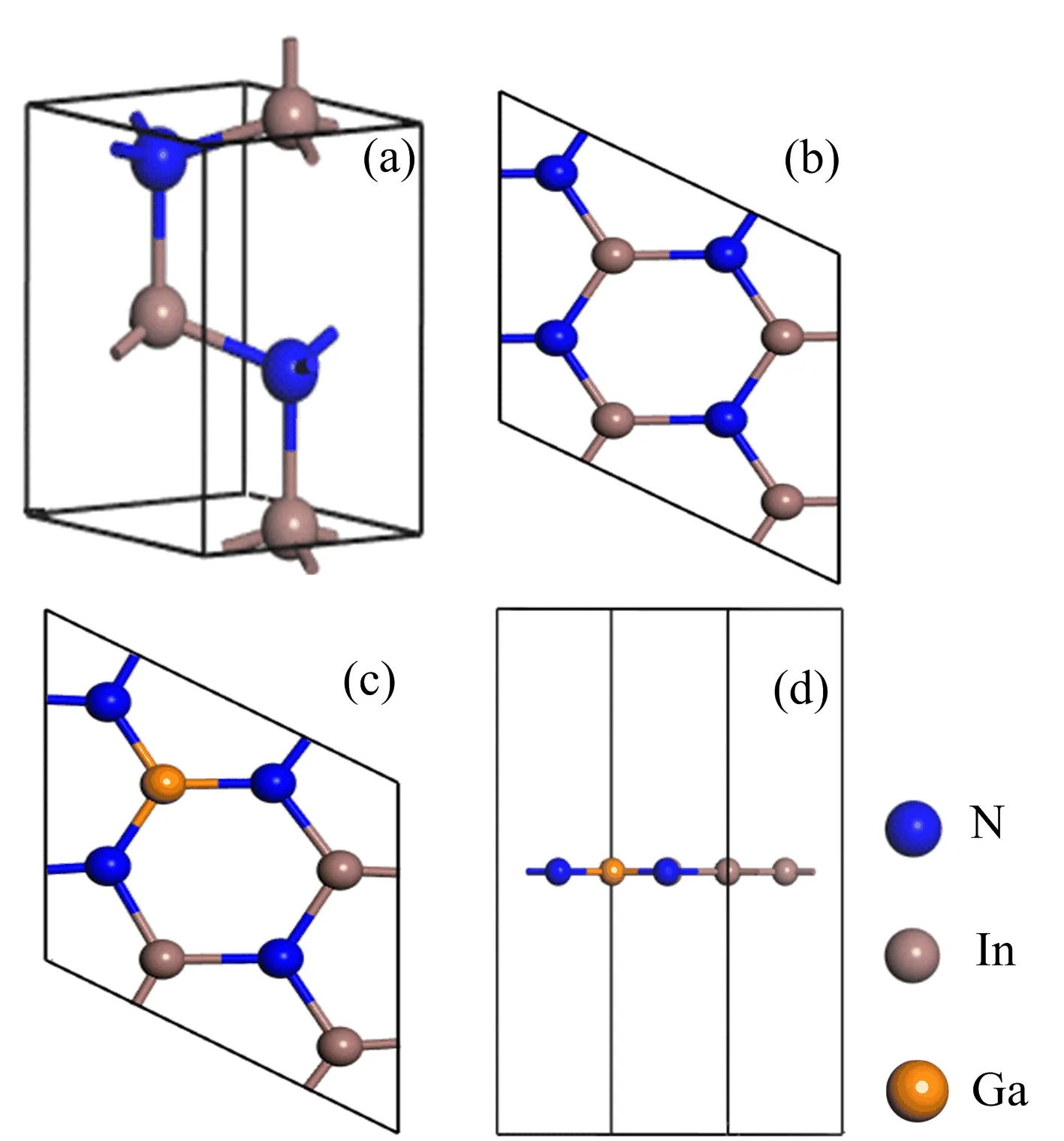
FIG.1 (a)Bulk InN,(b)single-layer InN,(c)single layer In0.75Ga0.25N,and(d)side view of single-layer In0.75Ga0.25N.
II.COMPUTATIONAL METHODS
In this work,we first test the band gap of bulk InN,and then mainly study the electronic structure and the optical properties of single-layer In1−xGaxN materials.Calculations are employed by the Vienna ab initio simulation package(VASP)[26,27]based on DFT,and the electron-ionic core interaction is represented by the projected augmented wave(PAW)potentials[28].The calculations on bulk InN and single-layer In1−xGaxN are performed using conventional Perdew Burke Ernzerhof(PBE)formulation of generalized gradient approximation(GGA)[29].However,the GGA underestimates the band gap value.Therefore,HSE functional is further performed to study both electronic and optical properties of bulk InN and single-layer In1−xGaxN,which is more accurate than GGA.Besides,the 5s24d105p1,4s24d104p1and 2s22p3states are considered as valence electrons for In,Ga and N atoms respectively.
In our work,the cutoff energy for the plane-waves is chosen to be 500 eV.For the test calculation of the bulk InN,the Brillouin zone is sampled using grids of 5×5×2 k-points[30],fast Fourier transformation(FFT)mesh value is 24×24×40,the iterative convergence accuracy is set to 1×10⁻⁵eV/atom.To deal with single-layer In1−xGaxN,we create the model of 2×2×1 supercell which contains 8 atoms,and a periodic boundary condition is applied to the supercell,the Brillouin zone is sampled by a set of 3×3×1,FFT mesh value is 48×48×125,and the supercell is large enough to ensure the vacuum space of 15˚A in order to eliminate the interaction between periodic images.The structures have been relaxed until the forces on each atom are smaller than 0.03 eV/˚A,and the convergence criteria for energies have been set to be 1.0×10⁻⁵eV.
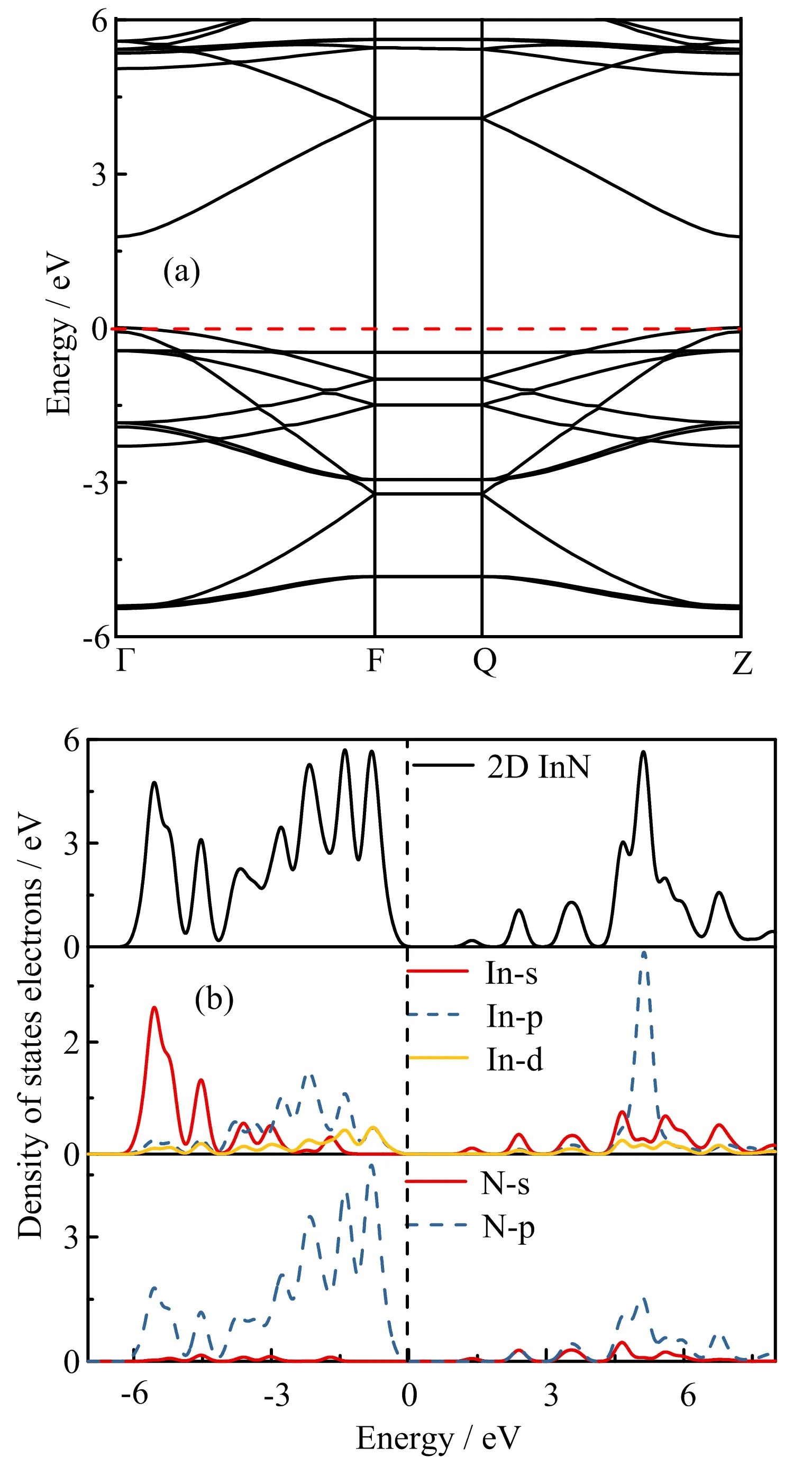
FIG.2 (a)Band structure and(b)DOS of single-layer InN.
III.RESULTS AND DISCUSSION
Our calculation models are shown in FIG.1,the lattice constants of single-layer InN are a=b=7.16˚A,c=15˚A and the N−In bond length is 2.073˚A,which is similar to the previous result[31].And the N−In bond length of single-layer InN is smaller than that of bulk InN(2.16˚A).In single-layer InN each N atom bonds with three In(sp2hybridization),but in the bulk InN each N atom bonds with four In atoms(sp3hybridization),and sp2bonds are stronger than the sp3bonds.When Ga doped single-layer InN,shown in FIG.1(c)and(d),the average bond length of N−In is 2.097˚A,and the average bond length of N−Ga is 1.888˚A due to the different electronegativity between In and Ga.Then we calculated the band structure of bulk InN with AEXX=0.3,which shows the band gap is 0.79 eV.Our result is very consistent with the experimental value,so we fix AEXX=0.3 for the following calculations.
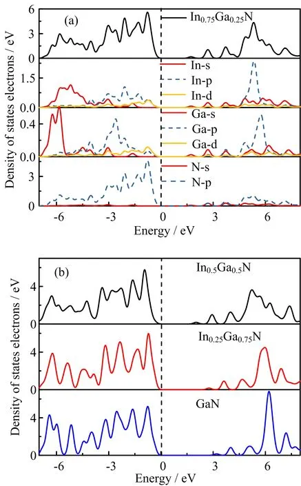
FIG.3 (a)DOS of In0.75Ga0.25N and(b)In1−xGaxN.
The band structure and DOS of single-layer InN are shown in FIG.2(a)and(b),respectively.The singlelayer InN shows semiconductivity with a direct band gap of 1.8 eV,which is bigger than the result of Nour et al.(1.66 eV)[31].According to FIG.2(b),the DOS of single-layer InN can be divided into 3 groups.The lowest energy group of valence band around−6 eV to−4 eV is mainly contributed by 5s-In and 2p-N states,and we can see that there is an overlap between 5s-In and 2p-N.The second group of valence band from−4 eV up to the Fermi level,the DOS is mainly originated from 5p-In,4d-In,2p-N states.These is a strong overlap between the 5p-In states and 2p-N states.It indicates that the bond between N and In is covalent.The third group from 0 eV to 6.3 eV is the unoccupied states,the DOS is mainly composed of 2p-N and 5s,5p-In states.
In order to further explore the effect of Ga doped concentration on the electronic properties and optical properties of single-layer InN monolayer nanosheets,we have calculated the DOS for different Ga doped concentration(In0.75Ga0.25N,In0.5Ga0.5N,In0.25Ga0.75N,and GaN),and we can clearly see from FIG.3 that for different Ga doping concentrations,the electronic structures have similar characteristics.For In0.75Ga0.25N(see FIG.3(a)),it can be seen that the DOS in the energy region(−6 eV to 0 eV)mainly consists of 2p-N and 5p states,4d-In states have a little contribution.Because of the low concentration of Ga atoms,the 4p,4d-Ga states also have a minimal contribution.From partial density of states(PDOS)of In,Ga and N,the 2p-N state is partially overlapped with the 5p-In state,which forms a hybrid effect and a stable covalent bond.Similarly,the p-state overlaps with 4p,4d-Ga states and also forms covalent bonds.
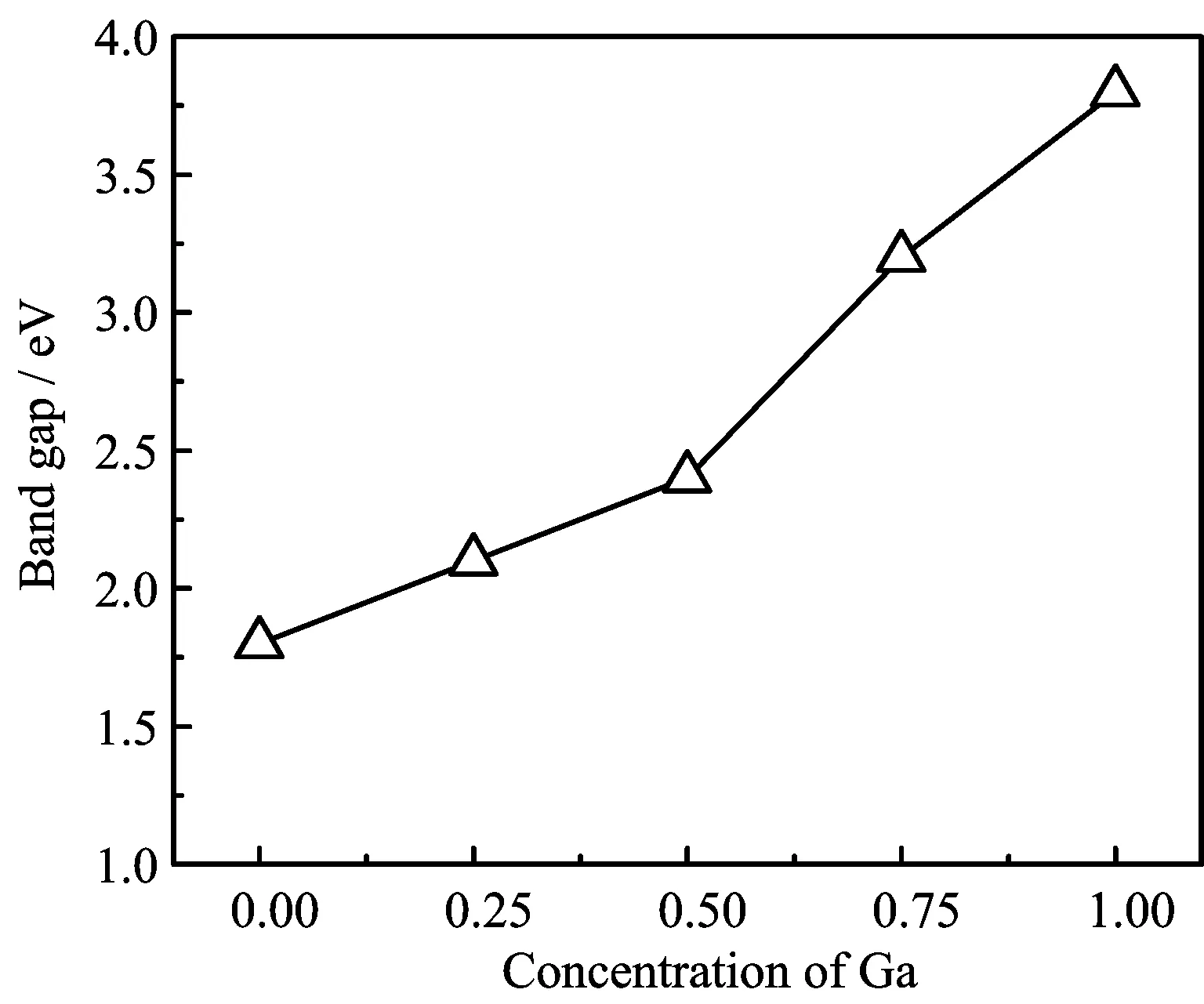
FIG.4 Band gap values of single-layer In1−xGaxN.
Compared with single-layer InN,the same point is that the valence band maximum of DOS of In0.75Ga0.25N is mainly contributed by the 2p-N and the 5p-In states,the difference is that there is part of the 4p-Ga involved in the contribution.With the increasing concentration of Ga doping(followed by 50%,75%,100%),as shown in FIG.3(b),when the concentration increases from 50%to 100%,the conduction band moves toward the high-energy part,resulting in a larger width of the optical band gap.The statistics of band gap values are shown in FIG.4.The result indicated that single-layer In1−xGaxN hybrid compounds can open considerable electronic gaps with the increase of Ga concentration.
Because the single-layer materials have huge application prospects in solar cells and optical devices[33,34],optical properties have attracted much attention for the single-layer materials.Complex dielectric function is the best physical quantity to understand the optical properties and it is a bridge between the micro-physical process and the solid electron structure of the band transition[35].Here,optical properties calculations are performed in the HSE using VASP code,and the polarized electric field is parallel to single-layer In1−xGaxN(E||x).The real and imaginary parts of dielectric function ε(ω)=ε1(ω)+iε2(ω)are calculated.By combining the dielectric peaks in the imaginary part of the dielectric function with the state density of the corresponding system,we can get the electron transition rules between the energy levels.
FIG.5(a)depicts the imaginary part of the dielectric element of the single-layer In1−xGaxN.All the peaks values in both directions are summarized in Table I.For single-layer InN from FIG.5(a)we can see four peaks,these peaks originate from transitions between occupied and unoccupied states,one locates around 1.8 eV that may be the transition of 5s-In states into 2p-N,another locates around 4 eV that could be the transition of 2p-N states into 5p-In states.When the concentration of Ga increases from 25%to 100%,the position of the main peaks moves in the direction of high energy without any notable shape changes,which is in good agreement with the increase of the band gap.Besides,from FIG.5(b),one can see that there has been a steep decline of ε1(ω)spectrum for single-layer In1−xGaxN when the frequency is in the range of 5−7 eV.
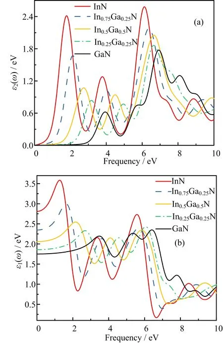
FIG.5 (a)The imaginary part of single-layer In1−xGaxN and(b)the real part of single-layer In1−xGaxN.
FIG.6(a)shows the refractive index of singlelayer In1−xGaxN.It can be seen from the figure that the static refractive index of pure single-layer InN is n0=1.69.When the photon energy increases,the refraction line shows a gentle trend.Moreover,with the increasing concentration of Ga doping,the n0of In1−xGaxN decreased from 1.69 to 1.32.FIG.6(b)shows the absorption coefficient of single-layer In1−xGaxN,we can see two main peaks at around 6.3 eV to 7.0 eV and 9.0 eV to 10.0 eV for the single-layer In1−xGaxN,and the peak intensity at around 6.3 eV is stronger than that at 9.0 eV.When the ratio x increases,both the refractive index and the absorption coefficient shift toward the higher-energy region.
IV.CONCLUSION
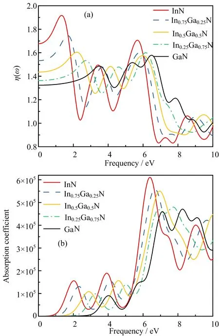
FIG.6 (a)The refractive index of single-layer In1−xGaxN and(b)the absorption coefficient of single-layer In1−xGaxN.

TABLE I The positions of main peaks of imaginary part of dielectric function of single-layer In1−xGaxN.
In summary,we studied the electronic and optical properties of single-layer In1−xGaxN.By using the first principles PAW potential under HSE method.The calculated InN band gap values are consistent with the experimental ones,and the results of band structure and DOS show that the In1−xGaxN nanosheet is a wide band gap semiconductor.Furthermore,with the increasing concentration of Ga doping,the band gap increases from 1.8 eV to 3.8 eV.Besides,the optical properties of In1−xGaxN monolayer nanosheets have been investigated,and the results show that the optical properties have a remarkable blue-shift as the concentration of Ga increases,which confirms that In1−xGaxN monolayer nanosheets have an excellent optical characteristics.
V.ACKNOWLEDGMENTS
This work was supported by the National Natural Science Foundation of China(No.11404230),Foundation of Science and Technology Bureau of Sichuan Province(No.2013JY0085).
[1]K.S.Novoselov,A.K.Geim,S.V.Morozov,D.Jiang,Y.Zhang,S.V.Dubonos,I.V.Grigorieva,and A.A.Firsov,Science 306,666(2004).
[2]F.X.Wang,C.S.Xue,H.Z.Zhuang,Y.J.Ai,L.F.Sun,Z.Z.Yang,and X.Zhang,Rare Metal.Mat.Eng.36,2020(2007).
[3]S.Strite and H.Morkoc,J.Vac.Sci.Technol.10,1237(1992).
[4]S.Nakamura,M.Senoh,N.Iwasa,and S.Nagahama,Appl.Phys.Lett.67,1868(1995).
[5]J.Simon,Z.Zhang,K.Goodman,H.Xing,T.Kosel,P.Fay,and D.Jena,Phys.Rev.Lett.103,026801(2009).
[6]S.Kako,C.Santori,K.Hoshino,S.Götzinger,Y.Yamamoto,and Y.Arakawa,Nat.Mater.5,887(2006).
[7]M.S.Miao,Q.Yan,C.G.Van de Walle,W.K.Lou,L.L.Li,and K.Chang,Phys.Rev.Lett.109,186803(2012).
[8]V.M.Polyakov and F.Schwierz,Appl.Phys.Lett.88,032101(2006).
[9]S.K.O.Leary,B.E.Foutz,M.S.Shur,U.V.Bhapkar,and L.F.Eastman,J.Appl.Phys.83,826(1998).
[10]B.E.Foutz,S.K.O’Leary,M.S.Shur,and L.F.Eastman,J.Appl.Phys.85,7727(1999).
[11]S.P.Fu and Y.F.Chen,Appl.Phys.Lett.85,1523(2004).
[12]D.Golberg,Y.Bando,Y.Huang,T.Terao,M.Mitome,C.Tang,and C.Zhi,ACS Nano 4,2979(2010).
[13]Y.H.Lee,X.Q.Zhang,W.Zhang,M.T.Chang,C.T.Lin,K.D.Chang,Y.C.Yu,J.T.W.Wang,C.S.Chang,L.J.Li,and T.W.Lin,Adv.Mater.24,2320(2012).
[14]J.Zhang,X.Liang,P.Zhang,K.Wu,G.Liu,and J.Sun,Acta Mater.66,302(2014).
[15]P.Tsipas,S.Kassavetis,D.Tsoutsou,E.Xenogiannopoulou,E.Golias,S.A.Giamini,C.Grazianetti,D.Chiappe,A.Molle,M.Fanciulli,and A.Dimoulas,Appl.Phys.Lett.103,666(2013).
[16]A.Sandhu,Nat.Phys.111,76(2006).
[17]T.T.Kang,X.Liu,R.Q.Zhang,W.G.Hu,G.Cong,F.A.Zhao,and Q.Zhu,Appl.Phys.Lett.89,2779(2006).
[18]E.Tiras,M.Gunes,N.Balkan,R.Airey,and W.J.Schaff,Appl.Phys.Lett.94,142108(2009).
[19]L.F.J.Piper,T.D.Veal,C.F.McConville,H.Lu,and W.J.Schaff,Appl.Phys.Lett.88,252109(2006).
[20]N.Miller,J.W.Ager III,H.M.Smith III,M.A.Mayer,K.M.Yu,E.E.Haller,W.Walukiewicz,W.J.Schaff,C.Gallinat,G.Koblmüller,and J.S.Speck,J.Appl.Phys.107,113712(2010).
[21]M.Kumar,T.N.Bhat,M.K.Rajpalke,B.Roul,N.Sinha,A.T.Kalghatgi,and S.B.Krupanidhi,Surf.Sci.605,L33(2011).
[22]Z.Y.Al Balushi,K.Wang,R.K.Ghosh,R.A.Vilá,S.M.Eichfeld,J.D.Caldwell,X.Qin,Y.C.Lin,P.A.DeSario,G.Stone,S.Subramanian,D.F.Paul,R.M.Wallace,S.Datta,J.M.Redwing,and J.A.Robinson,Nat.Mater.15,1166(2016).
[23]M.Y.Duan,L.He,M.Xu,M.Y.Xu,S.Xu,and K.Ostrikov,Phys.Rev.B 81,1718(2010).
[24]Q.Chen,M.Xu,H.Zhou,M.Duan,W.Zhu,and H.He,Phys.B 403,1666(2008).
[25]M.Y.Xu,M.Xu,M.Y.Duan,and Q.P.Hu,Chin.J.Chem.Phys.23,293(2010).
[26]G.Kresse and J.Furthmüller,Phys.Rev.B 54,11169(1996).
[27]G.Kresse and J.Hafner,Phys.Rev.B 49,14251(1994).
[28]G.Kresse and D.Joubert,Phys.Rev.B 59,1758(1999)
[29]J.P.Perdew,K.Burke,and M.Ernzerhof,Phys.Rev.Lett.77,3865(1996).
[30]H.J.Monkhorst and J.D.Pack,Phys.Rev.B 13,5188(1976).
[31]M.Ren,M.Li,C.Zhang,M.Yuan,P.Li,F.Li,W.Ji,and X.Liu,Phys.E 67,1(2014).
[32]N.Nouri and G.Rashedi,Phys.E 85,324(2017).
[33]H.Zheng,X.B.Li,N.K.Chen,S.Y.Xie,W.Q.Tian,Y.Chen,H.Xia,S.B.Zhang,and H.B.Sun,Phys.Rev.B 92,115307(2015).
[34]S.Nakamura,Science 281,956(1998).
[35]U.Rössler,Phys.Rev.184,733(1969).
 CHINESE JOURNAL OF CHEMICAL PHYSICS2018年3期
- CHINESE JOURNAL OF CHEMICAL PHYSICS的其它文章
- Network Modeling of Inflammatory Dynamics Induced by Biomass Smoke Leading to Chronic Obstructive Pulmonary Disease
- A Double Network Hydrogel with High Mechanical Strength and Shape Memory Properties
- A High-Performance and Flexible Chemical Structure&Data Search Engine Built on CouchDB&ElasticSearch
- Nucleation of Boron-Nitrogen on Transition Metal Surface:A First-Principles Investigation
- Maximum Thermodynamic Electrical Efficiency of Fuel Cell System and Results for Hydrogen,Methane,and Propane Fuels
- Electronic Structure and Optical Properties of K2Ti6O13Doped with Transition Metal Fe or Ag
