
Ultrafast Dynamics of Defect-Assisted Carrier Capture in MoS2Nanodots Investigated by Transient Absorption Spectroscopy
2018-06-27 06:48:10DaKeLaizhiSuiDunliLiuJianqiuCuiYunfengZhangQingyiLiSuyuLiYuanfeiJiangAnminChenJunlingSongMingxingJin
Da Ke,Lai-zhi Sui,Dun-li Liu,Jian-qiu Cui,Yun-feng Zhang,Qing-yi Li,Su-yu Li,Yuan-fei Jiang,An-min Chen∗,Jun-ling Song*,Ming-xing Jin*
a.Institute of Atomic and Molecular Physics,Jilin University,Changchun 130012,China
b.Jilin Provincial Key Laboratory of Applied Atomic and Molecular Spectroscopy,Jilin University,Changchun 130012,China
c.State Key Laboratory of Molecular Reaction Dynamics,Dalian Institute of Chemical Physics,Dalian 116023,China
d.School of Chemical&Material Engineering,Jiangnan University,Wuxi 214122,China
I.INTRODUCTION
Owing to the versatile applications of graphene in diverse fields,more and more graphene-like materials attracted increasing research attention[1].Among them,Molybdenum disulfide(MoS2)has become a popular material by virtue of particular structure and physicochemical character,such as good chemical stability,excellent mechanical flexibility,large specific surface area,and high carrier mobility[2].For graphene,the fact that the forbidden bandwidth is zero restricts the applications of some electronic devices[1,3].MoS2seems to be more suitable for optoelectronic device manufacturing due to the large intrinsic band gap and higher carrier mobility compared to graphene,which opens up new prospects of technological breakthroughs[4].The bulk or monolayer MoS2have exhibited great potential in optoelectronic applications[1,4].In addition,various aspects of low-dimensional MoS2materials including MoS2nanodots have been reported[2,5,6].It is suggested that the MoS2nanodots will be promising in the applications of optical and electronic devices.However,most of the existed investigations mainly focus on the fabrication of MoS2nanodots.The survey for exciton dynamics of MoS2nanodots remains less explored,which is of importance for exploiting their further applications.
The band gap width of MoS2can be adjusted by variation of layer thickness,ranging from 1.2 eV to 1.9 eV,due to the transition between Γ and K in the Brillouin zone of the MoS2[7].Such a phenomenon indicates that the precise control of the MoS2nanostructures on the morphology and size can affect greatly the physical characteristics of MoS2.Previous studies revealed the ultrafast processes of carrier in monolayer,few-layer,and bulk MoS2materials via femtosecond transient absorption spectroscopy,and different exciton relaxation processes were observed in a variety of MoS2materials[8–10].Contrasting two-dimensional layered materials in strict sense,MoS2nanodots have abundant edge states due to large surface area ratio,and the band gap width and the corresponding exciton binding energy increase as the size becomes smaller due to stronger quantum confinement effect in MoS2nanodots.Therefore,they may also exhibit distinct exciton relaxation dynamics from the layered or bulk MoS2[6–10].However,for all we know,ultrafast carrier dynamics of MoS2nanodots has been rarely reported.Transient absorption spectroscopy(TAS)is a powerful technique for exploration of ultrafast physical processes.TAS may provide more insights into the multiple and potentially interrelated carrier relaxation processes,which enable us to better understand the complicated ultrafast exciton dynamics of MoS2nanodots.
Herein,we focus on the relaxation processes of photoexcited carriers in MoS2nanodots via TAS.The transient absorption spectra of the sample under different pump fluences are surveyed.By globally fitting the experimental data,we reveal that defect-assisted carrier recombination processes we propose are well consistent with the observed dynamics.Meanwhile,Auger scattering is deemed to be the main mechanism of the photoexcited carrier transition.Our research will provide help and theoretical guidance for further application of MoS2materials.
II.EXPERIMENTS
All reagents were purchased commercially and used as received without further purification.MoS2nanodots were synthesized through a hydrothermal method according to the previous reported elsewhere with minor modifications[11].MoO3(12.0 mg),thioacetamide(14.0 mg)and urea(1.4 mg)were mixed in H2O(10.0 mL),and then stirred for 15 min.Finally,the mixture was then placed in an autoclave and kept at 240◦C for 12 h.Then the solution was rapidly cooled to room temperature.The resultant MoS2(1.0 mg/mL)was dispersed in an aqueous solution of sodium cholate(0.2 mg/mL),then,the dispersions were sonicated for 1 h.The dispersion was retained for use.The sample was characterized by JEM-2100F transmission electron microscope(TEM)performing at 200 kV.Steady-state absorption data were collected using AvaSpec-1650FUSB2 spectrometer.Coherent Libra regenerative amplifier Ti:sapphire laser was used to provide an initial light source for the time-resolved transient absorption measurement system.The output laser of the amplifier was 800 nm,1000 Hz,50 fs.The laser was divided into two beams:one was used to produce the pump pulses at the wavelength of 400 nm via the nonlinear frequency conversion of beta barium borate(BBO)crystal,and the other beam was focused into a sapphire plate to produce the probe pulses(450−700 nm).The sample was put in a 2 mm quartz cuvette,meanwhile the probe and pump beams were overlapped on the sample.The pump pulse was chopped at 500 Hz and the energy was adjusted by using a neutral density optical filter.The probe signals were collected by a fiber-coupled spectrometer(AvaSpec-1650F-USB2)and all measurements were carried out at room temperature.
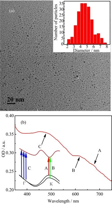
FIG.1 (a)TEM image of MoS2nanodots;inset is the particle size distribution of the sample.(b)Absorption signals of MoS2nanodots dispersed in water in a 2 mm cuvette.Inset is the schematic illustration for the A,B,C excitonic transitions.
III.RESULTS AND DISCUSSION
FIG.1(a)depicts the TEM image of MoS2nanodots,and the particle size distribution of the sample is inserted.It shows the size varying from∼2 nm to∼8 nm with the majority at around 5 nm.The corresponding absorption signals of the sample in 2 mm cuvette ranging from the UV to near infrared are shown in FIG.1(b).Resolved from the spectra,the characteristic absorption bands are similar to the other MoS2nanodots[12].The spectra are dominated by a feature signal at around 470 nm,as well as a smaller peak and its faint shoulder peak at around 620 and 670 nm.Three characteristic excitonic absorption bands are commonly labelled A(670 nm),B(620 nm),C(470 nm)[8,10].The A,B,and C bands are direct excitonic transitions between K and Γ[8,13,14].For the A(670 nm)and B(620 nm),both are corresponding to the K,deriving from the excitonic transitions of the spin-orbit split top valence band,around K and K′[15–17].For the conspicuous C peak(470 nm),it is ascribed to a weakly bound exciton,with a complex composition mainly resulting from interband transitions around Γ[13,16,18,19].

FIG.2 Transient absorption spectra of MoS2nanodots under pump fluences of(a)0.19 mJ/cm2,(b)0.32 mJ/cm2,(c)0.45 mJ/cm2,(d)0.57 mJ/cm2,(e)0.7 mJ/cm2,and(f)0.83 mJ/cm2.
FIG.2 exhibits the transient absorption spectra of MoS2nanodots recorded in the spectral region of 450−700 nm under different excitation pump fluences.The spectra show at least five apparent features,including two positive peak signals and three negative peak signals.Three negative peak signals appear at around 670,620,and 470 nm,which correspond to the A,B,and C excitons,respectively,and they agree well with the observed absorption peaks in FIG.1(b).They are mainly attributed to the ground state bleaching of A,B,and C.It is clear that the bleaching signals at around 470 nm are ascribed to the decrease of the electron density in the relevant position of the valence band after the C exciton is produced.However,as the dominant signal in the UV-visible absorption spectra,the C exciton(470 nm)exhibits a relatively weak bleaching signal compared with A(670 nm)and B(620 nm)excitons in the transient absorption spectra.The reason might be that the intervalley scattering processes in the region between K and Γ compensate for the partial decrease of the carriers in the valence band energy level correspond to the exciton C transition[20].When the pump fluences are relatively low,a positive signal from around 480 nm to 580 nm can be observed.It is due to excited state absorption in the conduction band involving the intersubband transitions[10,21–23].Meanwhile,an analogous positive signal appears in lowenergy region,which also originates from excited state absorption.It should be noted that,with increasing pump fluence,two separated excited state absorption signals aforementioned merge into a broad absorption band which contains two main peaks extending from 475 nm to 700 nm.The boundary of these two separated absorption signals is at∼620 nm,which corresponds to the B transition.When pump intensity is below 0.32 mJ/cm2,the positive signal disappears throughout the time window at∼620 nm.However,with increasing pump intensity,the excited state absorption signals appear,as shown in FIG.2(c)−(f).The phenomenon could be explained as the presence of the carriers in the higher level sub-bands of the conduction band.After photon excitation,the photo-excited carriers cool and relax to low level region of the conduction band.When pump intensity reaches a certain high level,the low level region is almost saturated.Thus,some photo-excited carriers would fill the higher subband levels in the conduction band.These carriers in the excited state absorb the probe pulse,thus new excited state absorption signals are produced.In addition,we observed the gradual shift of A,B peaks with the increase of delay time,a phenomenon consistent with previous reports[19,24],suggesting that the bandgap renormalization occurs in the process.
In order to understand the dynamics processes of MoS2nanodots,the evolution of dynamic curves under different pump intensity are exhibited in FIG.3.The evolution at 470 nm(C exciton)in FIG.3(a)shows the recovery process of ground state bleaching signals.According to the speed of the recovery process,we can tentatively divide the time scales of FIG.3(a)into two temporal regions:0−10 and 10−100 ps,respectively.When the sample is excited by the pump pulse,the transient absorption signals reach the maximum negative value within an extremely short time.A rapid recovery process appears within∼10 ps.Then a relatively gentle recovery process lasts for more than hundred picoseconds.The nonradiative recombination of electrons and holes in MoS2occurs mainly by two processes:direct band-to-band recombination and defect-assisted recombination[25].Direct band-to-band recombination is generally slow for MoS2,and it cannot result in the sudden transition on the recovery speed between time regions in the first 10 ps and the later 90 ps observed in FIG.3(a)[25,26].It indicates that a faster relaxation channel appears in the recombination process.Defectassisted recombination via carrier capture may play an import role in the relaxation processes.Phonon scattering and Auger scattering are the main mechanisms of carrier capture by defect states.Phonon scattering includes single phonon processes or multi-phonon processes,these processes all depend strongly on the lattice temperature and can affect the rate of carrier capture by defect states.In contrast,Auger scattering is usually not affected by lattice temperature[25–28].Since the excitation pulse was chopped at 500 Hz in our measurements,for the sample dispersed in water,the time gap between two pulses of 2 ms is long enough to dissipate efficiently heat accumulation generated by pump pulses.The influences of the lattice temperature induced by the pump irradiation with different intensity can be ignored.Therefore,the rate of carrier capture by defects mainly via phonon scattering is independent of pump intensity and is not consistent with our measurements.It suggests that Auger scattering is the dominant mechanism in the defectassisted recombination via carrier capture,and some higher order process,for instance,exciton-exciton annihilation accords with our observations:the recovery rate of the bleaching signals markedly accelerates after the pump intensity reaches a specific value[29].In addition,the dynamic curves show the sharp transition of the recovery rate at around 10 ps,which is not in agreement with the sole defect state.Due to the most semiconductors with multiple defects[30–33],different defects such as grain boundaries and dislocations in MoS2might be involved[25,34–37].According to the experimental results,we speculate that at least two different kinds of defects contribute to the fast and slow recovery processes.The analogous carrier capture model with different deep midgap defect levels was exhibited in monolayer MoS2and MoSe2[25,38].The recovery kinetics traces at 620 nm under different pump fluences(FIG.3(b))exhibit recovery processes of the bleaching signals when the pump fluences are relatively low.However,these traces exhibit the positive excited state absorption signals when the pump fluences are relatively high.It indicates that different pump fluences can lead to different relaxation pathways of photo-excited carriers in the exciton B evolution.When the photo-excited carrier density reaches a fixed value,the new excited state absorption signals increase with the pump intensity.For dynamic processes of A exciton,a fast recovery of the bleaching signals and a slow recovery of the excited state absorption signals are mixed(FIG.3(c)).Compared with the dynamic characteristics at 470 nm in FIG.3(a),similar pump fluence dependence appears in the recovery of the bleaching signals.The recoveries under pump fluences of 0.7 and 0.83 mJ/cm2are significantly faster than that under lower pump fluences.This may be attributed to the exciton-exciton annihilation under the pump fluences employed in the current experiment.
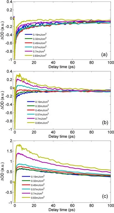
FIG.3 Normalized transient evolution dynamics of MoS2 nanodots under pump fluences of 0.19,0.32,0.45,0.57,0.7,0.83 mJ/cm2at(a)470 nm,(b)620 nm,and(c)670 nm in the first 100 ps.
To reveal the relaxation mechanism of the photoexcited carriers in MoS2nanodots,the experimental data were analyzed by a global fitting framework.The transient absorption data of our sample under different pump fluences were globally fitted using a model decay with single exponential.The decay associated difference spectra(DADS)and the corresponding parameters are acquired.Note that the shape and peak of the first DADS in FIG.4 are different,suggesting that the initial distribution of photo-excited thermal equilibrium carriers under different pump fluences is different due to the emergence of the saturated state at the low level region of conduction band.After photo-excited carriers undergo ultrafast thermalization within extremely short time,carrier cooling processes occur via intravalley relaxation and intervalley scattering of carriers to other valleys and sub-bands(FIG.5(a)).The process corresponds to the first lifetime τ1,the similar lifetime of carrier cooling(∼500 fs)and ultrafast thermalization processes,which have been shown in previous reports for monolayer and multilayer MoS2[25].The second lifetime τ2corresponds to the fast recombination of photo-excited carriers,which includes capture of photo-excited electrons at the bottom of the conduction band and photo-excited holes at the top of the valence band(FIG.5(b)).It can be found that τ2is similar under the relatively low pump fluences shown in Table I(0.19,0.32,and 0.45 mJ/cm2).Remarkably,when the pump fluences are relatively high(0.57,0.7,and 0.83 mJ/cm2),the lifetime τ2increases from(4.40±0.06)ps to(9.15±0.12)ps with the increasing of pump fluence.In combination with the inferences and defect-assisted carrier capture model mentioned above,the increase in τ2may be explained by saturation of the defect states.When the carrier density is high enough due to the increase in the pump fluence,a finite number of defect states need more time to complete the capture processes of photo-excited carriers,even though the high carrier density may increase the capture rate of carriers by the defect states.The third lifetime τ3corresponds to the slow recombination of photo-excited carriers by other defect states mentioned above.In the whole processes of carrier trapping,most of carriers are captured by the defects with relatively high carrier capture rate within τ2,and a small quantity of carriers is captured by the other kinds of defects with relatively low carrier capture rate within τ3(FIG.5(c)).Finally,the remaining small fraction of carriers relaxes via the direct interband electron-hole recombination(FIG.5(d)).This process corresponds to the fourth lifetime τ4(∼1 ns),which is similar to the lifetime of the same process in monolayer MoS2[39].
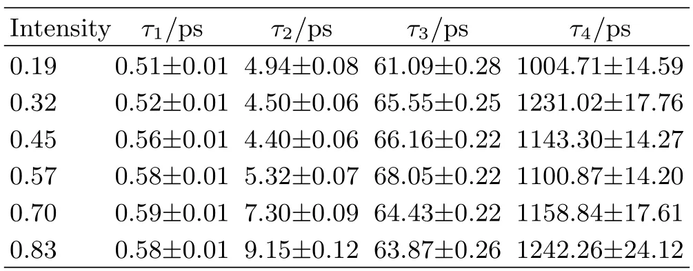
TABLE I Parameter values of the transient absorption signals of MoS2nanodots under different pump intensity(in mJ/cm2).
IV.CONCLUSION
In summary,we have surveyed the ultrafast exciton dynamics in MoS2nanodots by means of TAS.Experimental results show that the relaxation process of photo-excited carriers is not a simple direct band-toband recombination of electrons and holes.We deem that carrier capture by defects with different capture rates plays an important role in the observed dynamics.The proposed carrier capture model is well consistent with the features of the dynamics processes.Evidenced by the dependence of the dynamics processes on the pump fluence,Auger scattering has been revealed to be the main mechanism for nonradiative recombination and carrier capture by defects.The observed carrier relaxation dynamics may include four steps:carrier cooling,carrier fast capture by the defects,carrier slow capture by the other kinds of defects with relatively low carrier capture rate,and direct interband electronhole recombination.These findings may lead to deep insights into the fundamentals of carrier dynamics in MoS2nanodots,thus paving the way for their further applications.

FIG.5 Dynamic model of MoS2nanodots(a)after photoexcitation,carrier cooling occurs instantly and forms a correlated electron-hole plasma,(b)most of carriers are fast captured by the defects,then(c)a small quantity of carriers is captured by the other kinds of defects with relatively slow carrier capture rate,(d) finally,the remaining small fraction of carriers relaxes via direct interband electron-hole recombination.
V.ACKNOWLEDGEMENTS
This work was supported by the National Natural Science Foundation of China(No.11674128,No.21403232,No.11474129,and No.11504129),the Jilin Province Scientific and Technological Development Program,China(Grant No.20170101063JC),the Thirteenth Five-Year Scientific and Technological Research Project of the Education Department of Jilin Province,China(2016,No.400).
[1]N.Liu,P.Kim,H.K.Ji,J.H.Ye,S.Kim,and C.J.Lee,Acs Nano 8,6902(2014).
[2]L.Pei,S.Tao,H.Shu,and X.Song,Solid State Commun.218,25(2015).
[3]F.Schwierz,Proc.IEEE 101,1567(2013).
[4]X.Huang,Z.Zeng,and H.Zhang,Chem.Soc.Rev.44,1934(2013).
[5]B.Radisavljevic,M.B.Whitwick,and A.Kis,Acs Nano 5,9934(2011).
[6]B.Chakraborty,A.Bera,D.V.S.Muthu,S.Bhowmick,U.V.Waghmare,and A.K.Sood,Phys.Rev.B 85,396(2012).
[7]H.D.Ha,D.J.Han,J.S.Choi,M.Park,and T.S.Seo,Small 10,3858(2014).
[8]S.Aleithan,M.Livshits,S.Khadka,J.Rack,M.Kordesch,and E.Stinaff,Phys.Rev.B 94,035445(2016).
[9]N.Kumar,J.He,D.He,Y.Wang,and H.Zhao,J.Appl.Phys.113,10451(2013).
[10]Z.Nie,R.Long,J.S.Teguh,C.C.Huang,D.W.Hewak,E.K.L.Yeow,Z.Shen,O.V.Prezhdo,and Z.H.Loh,J.Phys.Chem.C 119,20698(2015).
[11]X.Geng,W.Sun,W.Wei,B.Chen,A.Alhilo,M.Benamara,H.Zhu,F.Watanabe,J.Cui,and T.Chen,Nature Commun.7,10672(2016).
[12]F.Liu,Y.Jiang,J.Yang,M.Hao,Z.Tong,L.Jiang,and Z.Wu,Chem.Commun.52,1867(2016).
[13]A.Carvalho,R.M.Ribeiro,and A.H.C.Neto,Phys.Rev.B 88,4807(2013).
[14]D.Kozawa,R.Kumar,A.Carvalho,A.K.Kumar,W.Zhao,S.Wang,M.Toh,R.M.Ribeiro,A.H.Castro Neto,and K.Matsuda,Nature Commun.5,4543(2014).
[15]A.Ramasubramaniam,Phys.Rev.B 86,2757(2012).
[16]D.Y.Qiu,J.F.Da,and S.G.Louie,Phys.Rev.Lett.111,216805(2013).
[17]T.Cheiwchanchamnangij and W.R.L.Lambrecht,Phys.Rev.B 85,205302(2012).
[18]D.Tsokkou,X.Yu,K.Sivula,and N.Banerji,J.Phys.Chem.C 120,23286(2016).
[19]G.Kime,M.A.Leontiadou,J.R.Brent,N.Savjani,P.OBrien,and D.Binks,J.Phys.Chem.C 121,22415(2017).
[20]A.Othonos,J.Appl.Phys.83,1789(1998).
[21]S.Sim,J.Park,J.G.Song,C.In,Y.S.Lee,H.Kim,and H.Choi,Phys.Rev.B 88,4521(2013).
[22]C.Mai,A.Barrette,Y.Yu,Y.G.Semenov,K.W.Kim,L.Cao,and K.Gundogdu,Nano Lett.14,202(2014).
[23]Z.Nie,R.Long,L.Sun,C.Huang,J.Zhang,Q.Xiong,D.W.Hewak,Z.Shen,X O.V.Prezhdo,and Z.Loh,Acs Nano 8,10931(2014).
[24]E.A.A.Pogna,M.Marsili,D.De Fazio,S.Dal Conte,C.Manzoni,D.Sangalli,D.Yoon,A.Lombardo,A.C.Ferrari,A.Marini,G.Cerullo,and D.Prezzi,ACS Nano 10,1182(2016).
[25]H.Wang,C.Zhang,and F.Rana,Nano Lett.15,339(2015).
[26]B.K.Ridley,Quantum Processes in Semiconductors,Oxford:Clarendon Press,(1982).
[27]M.Lax,Phys.Rev.119,1502(1960).
[28]C.H.Henry and D.V.Lang,Phys.Rev.B 15,989(1977).
[29]D.Sun,Y.Rao,G.A.Reider,G.Chen,Y.You,L.Brézin,A.R.Harutyunyan,and T.F.Heinz,Nano Lett.14,5625(2014).
[30]S.C.Choo,Phys.Rev.B 1,687(1970).
[31]J.S.Blakemore,Phys.Rev.110,1301(1958).
[32]G.K.Wertheim,Phys.Rev.109,1086(1958).
[33]J.A.Hornbeck and J.R.Haynes,Phys.Rev.97,311(1955).
[34]A.N.Enyashin,M.Barsadan,L.Houben,and G.Seifert,J.Phys.Chem.C 117,10842(2013).
[35]X.Liu,I.Balla,H.Bergeron,and M.C.Hersam,J.Phys.Chem.C 120,20798(2016).
[36]J.D.Fuhr,A.Saúl,and J.O.Sofo,Phys.Rev.Lett.92,026802(2004).
[37]N.Gao,Y.Guo,S.Zhou,Y.Bai,and J.Zhao,J.Phys.Chem.C 121,12261(2017).
[38]K.Chen,R.Ghosh,X.Meng,A.Roy,J.S.Kim,F.He,S.C.Mason,X.Xu,J.F.Lin,D.Akinwande,S.K.Banerjee,and Y.Wang,npj 2D Materials and Applications 1,15(2017).
[39]H.Shi,R.Yan,S.Bertolazzi,J.Brivio,B.Gao,A.Kis,D.Jena,H.G.Xing,and L.Huang,ACS Nano 7,1072(2013).
 CHINESE JOURNAL OF CHEMICAL PHYSICS2018年3期
- CHINESE JOURNAL OF CHEMICAL PHYSICS的其它文章
- Network Modeling of Inflammatory Dynamics Induced by Biomass Smoke Leading to Chronic Obstructive Pulmonary Disease
- A Double Network Hydrogel with High Mechanical Strength and Shape Memory Properties
- A High-Performance and Flexible Chemical Structure&Data Search Engine Built on CouchDB&ElasticSearch
- Nucleation of Boron-Nitrogen on Transition Metal Surface:A First-Principles Investigation
- Maximum Thermodynamic Electrical Efficiency of Fuel Cell System and Results for Hydrogen,Methane,and Propane Fuels
- Electronic Structure and Optical Properties of K2Ti6O13Doped with Transition Metal Fe or Ag