一款基于0.13 μm CMOS 工艺,0.1 GHz ~18 GHz 采用双反馈和噪声消除技术的低噪声放大器设计*
梁 元,张 弘
(西安电子科技大学宽禁带半导体材料与器件教育部重点实验室,西安710071)
Recently wireless system demands RF front-end module coping with increased wideband and flexibility.Due to various tradeoffs involved in RF circuit design the implementation of adaptive analog front-end seems to be more challenging than the adaptive digital backend.The advancement in device manufacturing technology has enabled the designers to integrate many transistors on a single chip for the realization of flexible circuits. In ultra-wideband(UWB)receiver front-end design,the UWB low-noise amplifier(LNA)is a critical block that receives small signals from the whole UWB band(3.1 GHz ~10.6 GHz)and amplifies them with a good signal-to-noise ratio property.In addition,high and flat power gain S21,good input and output impedance matching(i. e.,low S11and S22),and low noise figure(NF)performances across the whole UWB band are required.Besides,it is beneficial to design a LNA to possess greatly broadband functionality,which potentially accommodates large data rate transmission.The principal challenge is how to suppress NF and how to capture I/O matching over the wide band. As a result,in recently published literatures[1-3],high gain wideband low noises amplifiers(LNAs)have been in great interest. Finally,area consumption and power dissipation are other aspects that compromise the design of the LNA.The proposed LNA in this letter concentrates on comprehensive application scenarios.
This paper is organized as follow:section 1 represents the entire structure of the cascade LNA as well as analysis of each stage. Section 2 provides the performances and some discussions. Final conclusion will be given in section 3 to sum up this dissertation.
1 Circuit Illustration
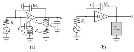
The proposed LNA is schematically presented in Fig.1.The entire structure is composed of two stages.The first stage,which includes M1-M4,source degenerated Lsand low Q inductive loads,employs double-feedback topology to extend the 3-dB bandwidth.For the sake of gain enhancement and noise cancellation,the second stage is adopted.The second stage is characterized by an inverter,followed by source follower.Shunt capacitance Csmakes sure that the active current source M9is short at radio frequency operation range.

Fig.1 The proposed cascade LNA

where H1(s)is the transfer function[See Fig.2(b)].


Fig.2 The simplified circuit of the first stage
Hypothesize that Coutis compensated by Lload,the input impedance can be modified as

As a start,assume Ls=0,that is,regardless of the inductive degeneration feedback,the Zin(s)is derived as

which is the traditional inductorless feedback utilizing active source follower as feedback network.Clearly,sCgswill deteriorate input matching at high frequencies.Following this inspection,alternative loop is established to compensate the degradation.Such a loop is also a feedback network,constructed by M2. Similarly,hypothesize that gM2=0,i. e. cut off the feedback loop established by M2.The input impedance can hence be written as

which is identical with the classical narrow band resonance topology using inductive degeneration[4].
Fig.3 shows the input impedance due to each feedback network alone with simultaneously the both ones due to each feedback mechanism alone,respectively,and the both ones.Note also that the forward gain of the first stage can be characterized by the transfer function H1(s).Even though shunt-peaking neutralizes Couteffectively,the frequency-dependent nature of inductive source degeneration in turn impacts on gain enhancement,even worsen at high frequency of operation. However,this gain reduction can be compensated by the second stage,which will be discussed later.The power gain performance of the first stage is shown in Fig.4.

Fig.3 Simulated input impedance of the first stage(Ω)

Fig.4 Simulated power gain of the first stage
Another threshold problem involves with the inductance of LD1. Since the operation frequency is broad,LD1should maintain a small value so that the first stage would not damage the entire power gain or avoid induced oscillation.Large inductance immediately results in larger inductor with many rings,which in turn potentially introduces more substrate noise and parasitic capacitance. In this design,the minimum dimension(width =3 μm,number of ring =1,rad =15 μm)of on-chip inductor is employed.Larger width leads to higher parasitic capacitance,and therefore results in greater swing in inductance.Lsof 150 pH is dictated.Lsis formed by dual paralleled minimum dimension inductors.Clearly,from Fig.4,the power gain sees a peak at around 10 GHz due to the inductive load,but eventually drops due to parasitic capacitance.More importunately,the double feedback induces more noise and provides lower gain,which necessitates cascade topology to release noise.
2018年11月7日,在金秋收获的日子里,哈挺在上海举办了新品发布会,哈挺最新的中国制造及全球智慧结晶产品——哈挺JONES & SHIPMAN 10精密外圆磨床在上海正式对外发布。出席本次发布会的嘉宾有哈挺全球CEO Chuck Dougherty先生、哈挺亚洲区总裁张静娟女士、哈挺全球及哈挺中国高层代表、合作伙伴及媒体朋友等百余位嘉宾。
Therefore,the realization of noise cancellation and gain enhancement depend on the second stage.Fig.5 illustrates the simplified schematic for noise cancellation illustration. For simplicity,hypothesize that Rs=50 Ω,i.e.the output impedance of the buffer stage of the first stage,including M5,M6,is well matched.Then we proceed by writing

where


Fig.5
Initially we assume that merely the channel thermal noise of active devices and of passive resistors take responsibility to the noise source.Gate induced noises are not included in calculation for facilitation. The thermal noise current Inflows out of M7,M8through node Y and node X,introducing the identical voltage sign at those two nodes.The voltage gain of the inverter,

where gM(s)is the equivalent combined trans-conductance of the PMOS and NMOS of the inverter,could be negative.It follows that,this difference in sign in terms of noise and signal makes it possible to cancel the noise of the matching device while simultaneously achieve desired signal summation.
The noise induced voltage at node X and Y are,respectively.

The output noise due to the matched device is therefore obtained as follow

Cancellation occurs when

Surprisingly,from equation(12),the noise cancellation condition is independent on the device performance or operation conditions,e.g.temperature,supply fluctuation.On the other hand,the overall voltage gain at the output terminal is given by

Fig.6 can be applied to calculate noise figure[NF=10lgF].Regardless of the noises originated from the current source,the load of the buffer of the second stage,and the isolation transistor M11,respectively.


Fig.6 The schematic for NF calculation

The noise figure of the second stage is displayed in Fig.7.From equation(19),numerical result shows NF =10lgF=125 dB if cancellation occurs,which is closed to the simulation one. (It has been assume that γ =2.0,which is an adequately precise approximation for short channel devices[4]).Besides,NF is well closed to NFmin.
Admittedly,any small signal that can be modeled by a current source between the drain and source of the matching device is cancelled as well(e. g.,1/f noise,thermal noise of the distributed gate resistance,and the bias noise current injected into node Y). However,the noise derived from Rfbis partially cancelled.

Fig.7 The NF characteristic of the second stage
It is instructive to investigate the transfer function of the second stage,which is known as the splitting-load peaking inverter.Ref.[1]indicates that Avfis expressed by

Therefore,the resultant poles from the proposed inductive splitting-load peaking inverter cell is,whose location has been boosted to a higher frequency as a requirement of bandwidth extension.Additional work is to implement a series peaking inductor preceding the buffer of the second stage,which renders the gain from node Y to the output terminal can be expressed as

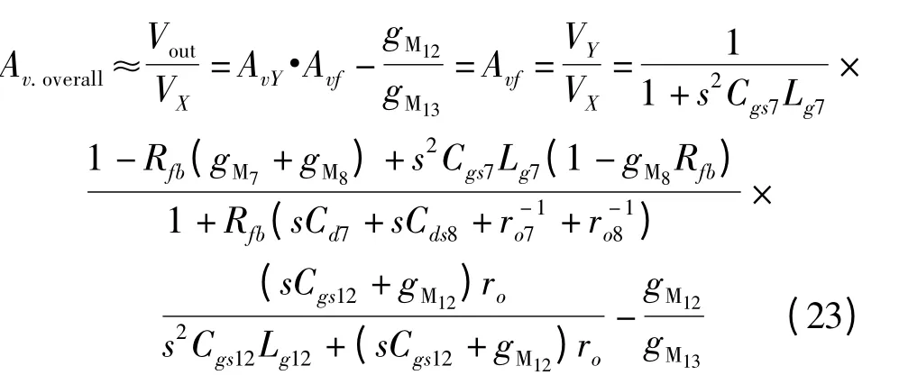
where ro=[1+(gM11+gMb11)ro11]ro10.Consequently,the peaking inductor in series with the gate of M12also plays a role of pushing the pole up to a higher frequency.Eventually,the overall gain from node X to the output terminal is acquired

It follows that Av.Y·Av.fcan be adequately large at high frequencies so that the gain decline due to the first stage could be compensated,or even inversed. Unfortunately however,the equivalent inductance of a physical inductor typically rises up with frequency,and then drops because of self-resonance.In practice,all inductors in this design are chosen with minimum width(3 μm)allowed by process so as to alleviate change and self-resonance characteristic. Such a consideration primary tries to find a broadband solution of stable and quasi-constant inductance,from which the high frequency operation does not necessary demands large inductor but rather small one to provide a peak.Shown in Fig.8,the above inductors create a peak response at high frequencies realm.This characteristic is significant in cascade topology design when the first stage suffers gain decline response. Fig.4 substantiates that this is the case.

Fig.8 The forward gain of the second stage
Our investigation also concerns the result of Fig.4,where the gain response is flat even at low frequencies.To corporate such an issue,an inevitable objective is to figure out whether the second stage can also be able to keep constant at the same frequency range.By scrutinizing Equation(19)~Equation(21),we find that gain flatness is done when some hypothesis and approximations are involved.Equation(21)is written as

Note that Cgs7Lg7is a small coefficient,so is Cgs12Lg12.So their corresponding s2terms can be neglected at low frequencies. Since Lg12is comparatively small,the buffer of the LNA is ideal and free of inductive influence also at low frequencies. Alternatively,we specify gM8Rfb≃1 in order that no strong frequency-dependent term exits at the numerator.Thus,the low-frequency response is therefore given as

Equ.(24)explains why the second stage is able to hold constant over low frequency range. Next,we investigate how the gain reacts to increasingly frequency. At this scenario,s2term becomes dominant as compared to other lower order counterparts.The numerator sees no parameters that are associated with frequency.Thus,the overall gain of the second stage at high frequencies can be expressed as

Adjusting the dimension of active devices and Lg7,12to ensure Cgs7Lg7≈(Cgs12Lg12)/(gM12ro). According to Ref. [1],Cgs7and Lg7should be adjusted becoming matched to the preceding stage,and Cgs12is directly proportional to the dimension of M12from which output matching is achieved. Thus,the only left parameters available to be set is Lg12.This is why and how Lg12can impact on the gain.As a result,equation(27)is modified as

This is the case explaining why the peak response occurs.
If Av(s)=Av.cis satisfied,the overall gain is

The forward gain of the second stage is shown in Fig.8.As observed,at high frequencies the second stage provides gain enhancement substantially.In addition,flat response at low frequencies is also captured.Noise suppression of the second stage is therefore enhanced because of the overall gain recovery at high frequencies from the second stage.In short,broadband gain flatness can be achieved by cascade configuration in which each stage provides gain contribution at uncorrelated frequency range.
2 Performancs and Discussions
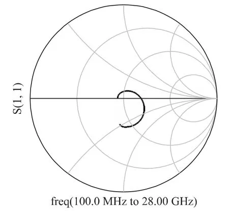
Fig. 9 shows the input reflection coefficient as Smith-chart form S11better than -10 dB is attained.Fig.10 displays the gain of the first stage,the second stage and the complete hierarchy,respectively. Gain bandwidth of 22 GHz is observed. Numerical result shows that the forward gain attains its maximum value 15.342 dB at 9.75 GHz meanwhile the minimum one 14.537 dB at 18 GHz. Thus,the maximum swing is merely 0.805 dB.Gain flatness within UWB is achieved gorgeously.Note that 9.75 GHz approximately accords with the poles generated by Cgs7Lg7and Cgs12Lg12.

Fig.9 The input reflection coefficient

Fig.10 The forward gain of the complete circuit
The output reflection coefficient is dominated by the buffer stage since 1/gM12=50 Ω is able to hold over the broadband.Unfortunately,the series peaking inductor Lg12will compensate and even take over the gate-source capacitive superiority of M12and therefore evidently affects the output matching at high frequencies. Inversely,the bandwidth of power gain enlarges with larger Lg12.Fig.11 demonstrates such a tradeoff.

Fig.11 Trade-off between gain bandwidth and output impedance matching(dB)
NF characteristic of each stage is displayed in Fig.12. Obviously,the second stage contributes lower noise at high frequencies.Besides,the first stage enjoys lower noise at low frequencies due to high gain. Thus,the cascade structure fulfills low noise figure within the band of operation. Numerical result shows that the NF ranges from 2.2 dB to 3.94 dB.

Fig.12 Noise figure of the corresponding stage
Fig.13 illustrates a two-tone test with 100 kHz frequency offset.IIP2=IIP3= -5 dBm and 1 dB desensitization point of -24 dBm at 9 GHz are presented.Distortions are mainly because of the nonlinearity from the common source stage M10~M12as well as incompletely complement inverter.Enlarging the overdrive voltage of M1is likely to release nonlinearity at the expense of more power consumption[7].

Table 1
3 Conclusion
In this study,a LNA using double feedback and noise cancellation technology is presented.Input impedance matching is captured by considering the doublefeedback topology as the first stage.The inverter as the second stage concurrently achieves noise cancellation and gain enhancement. The cascade configuration ensures broadband gain flatness. The performances of the proposed LNA presented in this dissertation as well as some recently published counterparts have been tabulated.Admittedly,some features of this proposed LNA perform availability for the state-of-the-art recommendations.
[1] Shih-Fong Chao,Jhe-Jia Kuo,Chong Liang Lin,et al.A 0.1 -11.5 GHz Low-Power[J]. Wideband Amplifier Using Splitting-Load Inductive Peaking Technique,2008:1531-1309.
[2] Wei-Hung Chen,Gang Liu,Boos Zdravko,et al. A Highly Linear Broadband CMOS LNA Employing Noise and Distortion Cancellation[J].IEEE Journal of Solid-State Circuits,2008,43(5).
[3] Behzad Razavi.RF Microelectronics[M].Prentice Hall PTR,Upper Saddle River,NJ 07458,ISBN 0-13-887571-5.
[4] Thomas H Lee. The Design of CMOS Radio-Frequency Integrated Circuits[M].Cambridge Uuiversity Press,2001.
[5] Shaeffer D K,Lee T H.A 1.2V 1.5GHz CMOS low noise amplifier[J].IEEE J.Solid-State Circuit,1997,32(5):745-759.
[6] Omid E Najari,Torkel Arnborg,Atila Alvandpour.Wideband Inductorless LNA Employing Simultaneous 2nd and 3rd Order Distortion Cancellation[J].978-1-4244-8973-2/10/2010 IEE.
[7] Li,Yuan J S. Linearity Analysis and Design Optimization 0.18pm CMOS RF Mixer for 0.18pm CMOS RF Mixer[J].IEE Proceedings Online no.20020355 DOE 10.1049/ip-cds:20020355.
[8] Omid E Najari,Torkel Arnborg,Atila Alvandpour.Wideband Inductorless LNA Employing Simultaneous 2nd and 3rd Order Distortion Cancellation[J].978-1-4244-8973-2/10/2010 IEEE.
[9] Li,Yuan J S. Linearity Analysis and Design Optimization 0.18μm CMOS RF Mixer[J]. IEE Proceedings Online no.20020355,DOE 10.1049/ip-cds:2002035.
[10] Chao S F,Kuo J J,Lin C L,et al. A DC -11.5 GHz Low-Power,Wideband Amplifier Using Splitting-Load Inductive Peaking Technique[J].IEEE Microw.Wireless Compon.Lett.,2008,18(7):482-484.
[11] Liao C F,Liu S I.A Broadband Noise-Canceling CMOS LNA for 3.1-10.6-GHz UWB Receivers[J].IEEE Journal of Solid-State Circuits,2007,42(2):329-330.

