
Switchable directional scattering based on spoof core–shell plasmonic structures
2022-05-16 07:09YunQiaoYin殷允桥HongWeiWu吴宏伟ShuLingCheng程淑玲andZongQiangSheng圣宗强
Chinese Physics B 2022年5期
Yun-Qiao Yin(殷允桥), Hong-Wei Wu(吴宏伟), Shu-Ling Cheng(程淑玲), and Zong-Qiang Sheng(圣宗强)
School of Mechanics and Photoelectric Physics,Anhui University of Science and Technology,Huainan 232001,China
Keywords: spoof core–shell plasmonic structures,directional scattering,switchable direction
1. Introduction
Light scattering from objects is a universal phenomenon regarding light–matter interactions. In order to explore the physics of interaction between light and subwavelength particles, Rayleigh and Mie conducted the pioneering researches many years ago.[1,2]As mentioned in the Mie scattering theory, the scattered fields of subwavelength objects can be attributed to electric and magnetic multipolar resonances. In addition, many fascinating and unique properties, such as transverse scattering,[3,4]nonscattering (scattering cancellation[5,6]and anapole[7]),superscattering,[8–10]and directional scattering,[11–14]have been investigated by tailoring the interference among electric and magnetic resonant modes. Of these,directional scattering has attracted the most considerable attention in recent years because of its unique properties in controlling and transforming the wavefront.
To achieve the directional electromagnetic scattering,Kerkeret al., in their pioneering work of 1983, theoretically proposed a hypothetical magnetic-dielectric particle, which exhibits electric and magnetic dipole resonance.[15]More importantly, the unidirectional forward or backward scattering was predicted to be due to the constructive interference of resonances enhancing the scattered intensity in one direction and the destructive interference minimizing scattering in the opposite direction. Recent years,optical metamaterials derive their novel capabilities from the interaction between light and various metallic nanostructures.These nanostructures exhibit artificial magnetism and their intrinsic electrical response,which makes it possible to achieve the directional light scattering in the visible and infrared regime.[16–19]However, the intrinsic Ohmic loss in metallic structure inevitably leads to low efficiency and limits the application of directional light scattering in realistic situation. To bypass the Ohmic dissipation, the high-index dielectric resonator, which supports inherently the strong magnetic and electric dipolar resonance at a high frequency with low absorption loss, is a promising candidate for the design of directional light scattering. Many theoretical and experimental researches have been reported that various dielectric structures are explored to achieve directional light scattering,such as nanosphere,[20–22]nanowire,[23]nanodisk,[24]and sphere/disk dimers.[25–27]In fact, all of the functions of directional scattering mentioned above are relatively simple. Inspired by the on-off mechanism of electric switches, optical switches are currently needed to block strong radiation. Thus, the directional scattering with adjustable switch is significant for the applications in sensing,detection, and digitizing electromagnetic wave for communication.
Moreover, to mimic the localized surface plasmons(LSPs)supported in metallic nanoparticles at optical frequencies, the concept of spoof LSPs has been proposed based on the textured perfect electric conductor at low frequencies.[28]Since then,many theoretical and experimental researches have been performed to investigate the electromagnetic property and applications of the spoof LSPs.[29–37]Comparing with the two-dimensional (2D) spoof plasmonic structure, the threedimensional (3D) textured perfect electric conductor (PEC)cylinder with finite thickness supports not only electric dipolar resonance,but also magnetic dipolar resonance on a deepsubwavelength scale.[38]Recently,we also have demonstrated that a hollow spoof plasmonic structure can support the magnetic and electric dipolar resonances similar to the Mieresonances in high-index dielectric particles.[39]Particularly,the resonant frequencies of the magnetic dipole and electric dipole can be freely tuned by changing the geometrical parameters. Furthermore, we demonstrate that directional electromagnetic scattering can be realized in an artificial Mie resonant structure that supports electric dipole mode and magnetic dipole mode simultaneously.[13]These results maybe provide a versatile platform to design the various advanced optical devices(antenna, metamaterial, metasurface,etc.) with switchable directional scattering direction.
In this work, we show that the structure is constructed by inserting a PEC cylinder into the hollow of the spoof plasmonic structure. Then, based on the modal expansion technique, we propose an effective medium theoretical model to analyze our structure. The results confirm the electromagnetic responses of the spoof core–shell plasmonic structures. Furthermore, it is verified that the directional scattering can be achieved due to the interference between electric dipole resonance and magnetic dipole resonance. Next, we discuss the influences of structure parameters on the backward and forward scattering. The results show that the directional scattering frequency and intensity can be tuned by tailoring PEC cylinder radius. Finally,the direction of directional scattering is switched by plugging a PEC cylinder core. The results indicate that we can use a simple method to switch the directional scattering direction.The proposed switchable directional scattering could open up an alternative avenue to digitizing electromagnetic wave communication and associated applications.
2. Spoof core–shell plasmonic structure
We consider that the spoof core–shell plasmonic structure with switchable directional scattering direction is constructed by inserting the PEC cylinder with the radius ofR1into the hollow of the spoof plasmonic structure as shown in Fig.1(a),and the core–shell structure is excited by a plane wave from the top. The proposed spoof plasmonic structure with a PEC core in the 2D scenario is schematically shown in Fig. 1(b).The proposed core–shell structure was constructed by periodically inserting cut-through slits into the hollow PEC cylinder. The outer radius and inner radius corresponding to the opening and bottom of the cut-through slits are represented asR3andR2, respectively. The (r,θ) are the polar coordinates,aandd=2πR3/mare the width of the slit and the period,respectively, wheremis the number of slits. The slits with depthh=R3-R2are filled with a dielectric with refractive index ofng,and the surround of this structure is air. As is well known,the region(R2<r <R3)can also be regarded as a homogeneous and anisotropic metamaterial of thicknesshwithεr=-∞,εθ=n2gd/a, anduz=a/dfor the transverse magnetic(TM)polarized incident wave. These structural parameters are illustrated in detail in Fig.1(b). In the following, the structure parameters are chosen asR2=15 μm,R3=30 μm,m=12,ng=3.4, anda=0.4d, unless otherwise specified in this work. The reason why we choose the refractive indexng=3.4 of dielectric here is to approach to the refractive index of silicon. The size of the unit cell can be designed on a deep subwavelength scale due to the limit ofa <d ≪λ0,whereλ0is the wavelength of the incident wave.

Fig.1. (a)Schematic diagram of spoof plasmonic structure with PEC cylinder,with TM-polarized incident plane wave propagating from top to bottom along y direction. (b)Two-dimensional structure with structural parameters:inner and outer radii of the spoof plasmonic structure R2 and R3,periodicity d, and slit width a, and PEC cylinder radius R1. Cyan region and yellow region represent Si and PEC materials.
3. Results and discussion
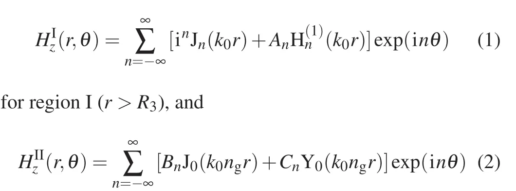
Generally, the scattering cross section (SCS) can accurately describe the electromagnetic response of the structure with negligible absorptions. Therefore, we show the normalized SCS(denoted by black dotted line)by the finite element method(FEM)with the commercial software COMSOL Multiphysics in Fig. 2(a). The SCS is normalized to the diameter 2R3of the core–shell structure. It is obvious that we can clearly see three resonant peaks in the SCS spectrum,which respectively correspond to magnetic dipole(MD),electric dipole (ED) and electric quadrupole (EQ). Then, based on the modal expansion technique, we propose an effective medium theoretical model to analyze our structure and can write the magnetic fieldHzin different regions as
for region II(R2<r <R3),and


with
whereM=[Jn(k0R2)-J′n(k0R1)Yn(k0R2)/Y′n(k0R1)] andN=[J′n(k0R2)-J′n(k0R1)Y′n(k0R2)/Y′n(k0R1)]. In this example, the analytical total SCS (marked by red solid line) is determined by Eq. (4). Then, we calculate the individual SCS of multipolar resonances as shown by the green solid line(n=0,MD),blue solid line(n=±1,ED),and cyan solid line(n=±2,EQ).
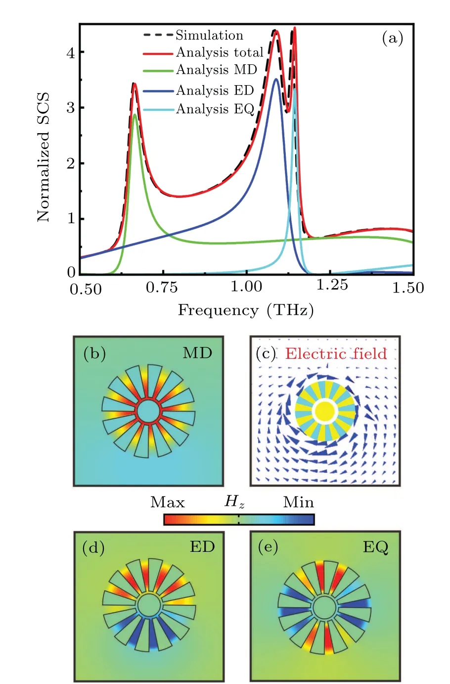
Fig. 2. (a) Calculated SCS spectra for the spoof plasmonic structure with PEC cylinder, with black dotted line corresponding to simulation result and red solid line being analytic calculation. Green solid line,blue solid line,and cyan solid line referring to SCS of modes MD,ED,and EQ,respectively. (b)Distribution of magnetic field Hz at the resonant frequency of MD mode in the structure. (c)Distribution of electric field marked by blue arrows. (d)and(e)Distribution of magnetic field Hz at the resonant frequency of ED and EQ modes in the structure.
To clearly demonstrate the resonant nature, the distributions of magnetic fields corresponding to three resonant peaks in the SCS spectrum,which is in thezdirection,are illustrated in Figs.2(b),2(d),and 2(e). Particularly,the electric field distribution denoted as blue arrows is also given in Fig.2(c)corresponding to the MD mode. These results clearly confirm the electromagnetic responses of the spoof core–shell plasmonic structures.
The proposed spoof plasmonic structure with PEC core in the 2D scenario is schematically shown in Fig. 3(a). The TM-polarized incident wave from the top is excited and the scattered into the lower (forward) or upper (backward) part.Next, we will discuss the scattering properties from the designed structure as shown in Fig.3(b).In Fig.3(b),the red and black solid lines indicate the backward and forward scattering cross sections respectively. The blue solid line represents the forward-to-backward(F/B)ratio. We notice that the backward scattering is almost zero and the F/B ratio has a maximum value atf=0.63 THz in Fig. 3(b), denoted as “1”. Moreover,atf=0.75 THz denoted by vertical dotted line“2”,the backward scattering is dominant and the F/B ratio is minimum.To demonstrate this,we plot the angular scattering diagram in Figs. 3(c) and 3(d) denoted as “1” and “2” corresponding to those in Fig.3(b). For the scattered coefficients from Eq.(4),we obtain the angular scattering amplitude of far-field

whereθis the polar angle.In our case,the multipole number isn=0,1,2 corresponding to MD,ED,QD.In Fig.3(c),we can see that the scattering farfield(red solid line)calculated from Eq.(6)shows the distribution of directional forward scattering,and simultaneously the far-field scattering is demonstrated by numerical simulation(marked by the black cross symbols). It is obvious that the scattering light from the spoof plasmonic structure is almost transformed into forward scattering and barely no backward scattering. Similarly,the farfield distribution of directional backward scattering is plotted in Fig.3(d).The result indicates that the scattering light is almost transformed into backward scattering and low forward scattering.The physical mechanism behind directional forward scattering is that the constructive interference between the scattering fields of MD mode and ED mode occurs in the forward direction forf=0.63 THz, while destructive interference occurs in the backward direction. In other words,the backward scattering amplitude is required to be zero,i.e.,S(180°)=0,then we can obtain the first Kerker condition: Re(A0)=Re(2A1)and Im(A0)=Im(2A1). While the constructive interference between the scattering fields of MD mode and ED mode occur in the backward direction for directional backward scattering atf=0.75 THz,the destructive interference occurs in the forward direction. Then, we can also obtain the second Kerker condition from Eq.(6)forS(0°)=0,i.e.,Re(A0)=Re(2A1)and Im(A0)=-Im(2A1).
Fig.3. (a)TM-polarized incident plane wave propagating from top to bottom along y direction. (b) Forward (black curve) and the backward (red curve) scattering cross-sections, and the forward-to-backward ratio (blue curve) of the structure. (c) and (d) Far-field scattering patterns at the two spectral points corresponding to the vertical dashed lines in panel (b) denoted by“1”and“2”.
In the above discussion, we have proved that the directional electromagnetic scattering can be induced due to the mutual interference and simultaneous excitation of magnetic dipole,electric dipole,and electric quadrupole. Next,we will discuss the influences of structure parameters of the core–shell structure on the backward and forward scattering. In order to achieve the switch design,we must discuss the scattering characteristics of the PEC bolt radius change. Figure 4(a) shows the individual SCSs of multipolar resonances represented by red(MD),blue(ED),and black(EQ)solid lines,respectively.When the other parametric conditions remain unchanged, we consider six structural models by varyingR1from 12 mm to 15 mm. Then the corresponding scattering cross section are plotted in Figs.4(a1)–4(a6).We can observe that the magnetic and electric resonance frequencies are gradually approaching to each other with the radius increasing. The magnetic dipolar mode is blue-shifted and both electric dipolar mode and quadrupole mode are red-shifted. Clearly, both the directional forward scattering and the backward scattering will be enhanced because the interference between magnetic dipole and electrical dipole is enhanced as indicated in Figs. 4(a1)–4(a4). Although the increasing of the PEC bolt radius can enhance the directional forward scattering, it will not produce the directional backward scattering because the mutual interference among the magnetic dipole, electric dipole and electric quadrupole. In addition,the angular scattering diagram of the directional forward scattering is shown in Fig.4(b). Then the corresponding backward scattering is plotted in Fig.4(c).These results show that we can tune freely the directional scattering frequency and radiation intensity by tailoring the geometrical parameters.

Fig.4.(a)Individual SCS of multipolar resonance represented by red(MD),blue(ED),and black(EQ)solid lines for designer structures with different values of PEC cylinder radius R1 in panels(a1)–(a6). (b)Far-feild forward scattering patterns from F1 to F6 in panel(a). (c)Far-feild backward scattering patterns from B1 to B4 in panel(a).
That the interference between electric dipole resonance and magnetic dipolar resonance causes the directional electromagnetic scattering is clearly shown in the above analysis.Next,the unique feature with switchable directional scattering direction will be shown. Firstly, we consider a hollow PEC cylinder with periodic cut-through slits as shown in Fig.5(a).Then,we also calculate the individual SCS of multipolar resonances represented by red(MD)and blue(ED)solid lines in Fig.5(c). We can see that the directional scattering occurs at the overlap of the two curves.The intersection on the left is the directional forward scattering and the right is the directional backward scattering. Meanwhile, the angular scattering diagram of directional backward scattering is plotted in Fig.5(e).For convenience,we refer to this state as“Turn on”. Next,in order to achieve the state switching,we insert a PEC cylinder with the radius ofR1into the cavity of the structure as indicated in Fig.5(b). From the above discussion,we can change the directional scattering frequency by changing the radiusR1.Therefore,we have moved the forward scattering frequency to an operating frequency the same as the operating frequency of the backward scattering in Fig. 5(c). Furthermore, the angular scattering diagram of directional forward scattering is also shown in Fig. 5(f) and this state is referred to as “Turn off”.In order to determine whether the directional scattering have occurred,we plot the field distribution of“Turn on”and“Turn off”in Figs.5(g)and 5(h). The white arrow indicates the direction of the incident wave, and the small black spot in the plot corresponds to the structure. According to the field distribution,we can find that the structure achieves the switching of directional scattering direction due to the insertion of PEC cylinder.
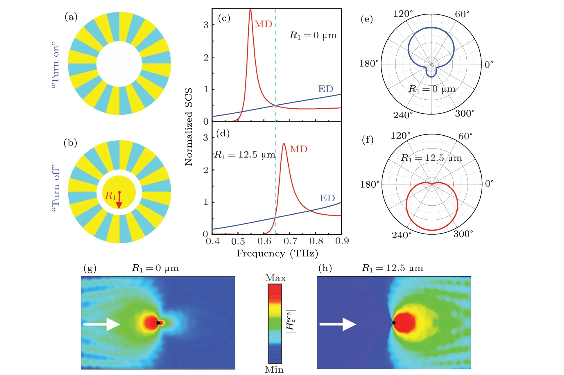
Fig.5. (a)Schematic diagram of spoof plasmonic structure with PEC cylinder,with this state referred to as“Turn on”. (b)Schematic diagram of inserting PEC cylinder into the center of the structure in panel(a), with this state referred to as“Turn off”. (c)and(d)Individual SCS of multipolar resonances represented by red(MD)and blue(ED)solid lines for the designer structures in panels(a)and(b). (e)and(f)Far-field scattering patterns in two states. (g)and(h)Near-field distributions in two states.
4. Conclusions
In this work, we have demonstrated that the spoof Mie resonant structure can present the directional scattering by the interference between the electric dipole resonanceand magnetic dipole resonance on a deep-subwavelength scale. By modal analysis and numerical simulation,we confirm the electromagnetic responses of the spoof Mie resonant structures,which states that the structure can achieve the directional forward scattering and backward scattering. In addition,we also discuss the influence of PEC cylinder radius on the performance of the directional scattering. Finally, we achieve the switching of directional scattering direction by inserting a PEC cylinder into the hollow of the spoof plasmonic structure. In addition, the proposed structure can be achieved by dry or wet etching process,such as e-beam lithography,Focused ion beam lithography,and reactive ion etching,The proposed active tunable concept could open up an alternative avenue to manipulating and controlling electromagnetic scattering in microwave and terahertz region.
Acknowledgements
Project supported by the National Natural Science Foundation of China (Grant No. 11904008), the Natural Science Foundation of Anhui Province, China (Grant No. 1908085QA21), and the China Postdoctoral Science Foundation(Grant No.2019M662132).

- Chinese Physics B的其它文章
- A nonlocal Boussinesq equation: Multiple-soliton solutions and symmetry analysis
- Correlation and trust mechanism-based rumor propagation model in complex social networks
- Gauss quadrature based finite temperature Lanczos method
- Experimental realization of quantum controlled teleportation of arbitrary two-qubit state via a five-qubit entangled state
- Self-error-rejecting multipartite entanglement purification for electron systems assisted by quantum-dot spins in optical microcavities
- Pseudospin symmetric solutions of the Dirac equation with the modified Rosen–Morse potential using Nikiforov–Uvarov method and supersymmetric quantum mechanics approach