
Enhancement of fMAX of InP-based HEMTs by double-recessed offset gate process
2022-05-16 07:12BoWang王博PengDing丁芃RuiZeFeng封瑞泽ShuRuiCao曹书睿HaoMiaoWei魏浩淼TongLiu刘桐XiaoYuLiu刘晓宇HaiOuLi李海鸥andZhiJin金智
Chinese Physics B 2022年5期
Bo Wang(王博) Peng Ding(丁芃) Rui-Ze Feng(封瑞泽) Shu-Rui Cao(曹书睿)Hao-Miao Wei(魏浩淼) Tong Liu(刘桐) Xiao-Yu Liu(刘晓宇) Hai-Ou Li(李海鸥) and Zhi Jin(金智)
1Guangxi Key Laboratory of Precision Navigation Technology and Application,Guilin University of Electronic Technology,Guilin 541004,China
2High-Frequency High-Voltage Device and Integrated Circuits Center,Institute of Microelectronics,Chinese Academy of Sciences,Beijing 100029,China
Keywords: InP,HEMT,maximum oscillation frequency(fMAX),double-recess,offset gate
1. Introduction
InP-based high electron mobility transistors(HEMTs)are regarded as the most promising candidates for millimeterwave integrated circuits (MMIC) and even terahertz monolithic integrated circuits (TMIC) because of their extremely excellent high-frequency, high-gain and low-noise characteristics.[1–4]They play key roles in radio-astronomy and deep-space communication. In recent years, the requirements for higher operation frequency and larger output power of TMIC result in a strong push of THz transistor technologies with high cut-off frequency(fT)and maximum oscillation frequency (fMAX).[4–9]ThefMAXof InP-based HEMTs were mainly improved by scaling down the gate length.[10]Laiet al. reported the first InP-based HEMT with afMAXexceeding 1 THz by reducing the gate length to 50 nm.[4]Meiet al. demonstrated 25 nm gate length InP-based HEMTs withfMAXof 1.5 THz and realized the first TMIC with 1 THz amplification.[8]However, the gate length is seriously limited by the available lithography technology. At present, it is difficult to increasefMAXby continuously reducing the gate length. Another way to improve thefMAXis to optimize parasitic effects. Various efforts have been made in this regard,such as reducing the source-to-drain spacing (LSD),[11]gateto-channel distance (tins),[12]as well as optimizing the gate recess,[9,13,14]and the gate stem height.[15,16]
In this paper, we will report on a novel double-recessed offset gate process for improving thefMAXof InP-based HEMT instead of a gate scaling that would often be used to obtain high RF performance. A double-recess gate structure has been used previously in GaAs-based HEMTs to improve breakdown voltage, which in turn increases output power.[17]We form the double-recess gate structure by selectively etching the cap layers. Compared with the traditional doublerecess gate structure,the incompletely removed cap layer can effectively reduce the exposed area of the active region and inhibit the surface effects. By controlling the gate offset,the parasitic effects can be further optimized for improved performances. Single-recessed HEMTs, and double-recessed HEMTs with different gate offsets have been fabricated and characterized. In addition,the parasitic parameters of devices are extracted and analyzed by using the small-signal model,which explains the influence of the double-recessed offset gate process.
2. Experiment
The schematic cross-section of double-recessed InPbased HEMTs is shown in Fig. 1. The epitaxial layers of the devices were grown by gas source molecular beam epitaxy (GSMBE) on 3 inch semi-insulating InP(100) substrates. From bottom to top, the layers consist of a 500 nm In0.52Al0.48As buffer layer, a 15 nm In0.53Ga0.47As channel layer,a 3 nm unstrained ln0.52Al0.48As spacer layer, a Si delta doping layer with 5×1012cm-2doping concentration, an 8 nm unstrained ln0.52Al0.48As Schottky barrier layer, a 4 nm InP etch-stop layer for preventing over etching and a 15 nm/15 nm/10 nm Sidoped ln0.52Al0.48As/In0.53Ga0.47As/In0.65Ga0.35As composite contact layer with a concentration of 1×1019cm-3/1×1019cm-3/3×1019cm-3. The 10 nm strained and heavily doped In0.65Ga0.35As layer to reduce the actual metal-semiconductor contact resistance, a 15 nm heavily doped In0.53Ga0.47As layer, and a 15 nm heavily doped ln0.52Al0.48As layer to lower the potential barrier across the Schottky barrier layer in the source and drain access regions.[18,19]Hall measurements were made at the room temperature,showing a carrier mobility of over 10000 cm2/(V·s).

Fig.1. Schematic cross-section of double-recessed InP-based HEMTs.
The fabrication process of double-recessed InP HEMTs mainly contains five steps, including mesa isolation, ohmic contact formation,gate recesses,T-gates and connection pads.Firstly, isolating mesa was formed by utilizing phosphorus acid-based wet chemical etching. Next, the source and drain were spaced 2.4 μm through a lithography process,followed by Ti/Pt/Au (15 nm/15 nm/50 nm) evaporated to satisfy the requirement of Ohmic contact by electron beam evaporation without annealing.
Afterward, the 0.8 μm first gate recess was defined by electronic beam lithography (EBL) with a ZEP520A e-beam resist layer, and the In0.65Ga0.35As/In0.53Ga0.47As cap layers were etched by a citric acid based solution with an etch selectivity of 20:1 to In0.52Al0.48As. The distance between the source and drain from the center of the first gate recess is 0.9 μm and 1.5 μm, respectively. The source-side recess length (Lrs) and the drain-side recess length (Lrd) are controlled by adjusting the position of the T-shaped gate to form symmetrical or asymmetric gate recess. T-gates were defined by EBL with a PMMA/Al/UVIII (200 nm/10 nm/800 nm) ebeam resist stack. The top UVIII was exposed by a small dose and wide line, then developed by TMAH and rinsed in DI water to determine the gate cap. And then the bottom PMMA was exposed by a big dose and narrow line,then developed by 1, 2-dimethylbenzene to define the gate foot. After that, the second gate recess was etched in the In0.52Al0.48As cap layer by a phosphate based solution, and a Ti/Pt/Au(25 nm/25 nm/300 nm)metal stack was evaporated and lifted off. Three different gate positions were used to observe the dependence of RF performance on gate offset. The gate was located at the first gate recess center, with an offset to the source or drain side. The gate length of all devices is 100 nm,as shown in Fig.2.Finally,the Ti/Au(15 nm/300 nm)connection pads were evaporated for on-wafer DC and RF characteristics measurements.
Single- and double-recessed HEMTs were identically processed, except for additional recess etching. The detailed parameters of fabricated HEMTs are shown in Table 1. All devices were deposited by plasma-enhanced chemical vapor deposition(PECVD)with 20 nm Si3N4as a passivation layer.

Fig.2. SEM photograph of the T-Gate and gate recesses of the HEMTs.
Table 1. The detailed parameters of fabricated HEMTs.
3. Results and discussion
3.1. Double-recessed structure
DC properties were characterized by using a HP4142 semiconductor parameter analyzer at the room temperature.Figure 3 shows theID–VDoutput characteristics and transfer characteristics of the single-recessed HEMTs (device A) and double-recessed HEMTs (device B). Due to the higher series resistances,such as the source and drain resistance(RsandRd)caused by the removal of more cap layer during the formation of the first gate recess, the double-recessed HEMTs exhibit lower maximum drain–source current (ID,max) and maximum extrinsic transconductance (gm,max) than the single-recessed HEMTs. Extrinsic transconductancegmis expressed by

wheregm,intis the intrinsic transconductance of the HEMTs.It can be seen from Eq.(1)that the increase ofRswill lead to a significant decrease ofgm,max.
The RF performance is characterized via an Agilent E8363B PNA vector network analyzer from 0.1 GHz to 40 GHz. Before measurement,the devices were de-embedded by using on-wafer open and short pad structures to exclude the parasitic effect. Figure 4 shows the H21and MAG/MSG versus frequency of the single-recessed HEMTs (device A)and double-recessed HEMTs (device B) at their respectivegm,maxpoints. Since the test frequency range was limited from 0.1 GHz to 40 GHz, thefTandfMAXwere obtained by extrapolating the curve of H21and MAG/MSG followed by a slope of-20 dB/dec, respectively. ThefTand thefMAXof single-recessed HEMTs are 296 GHz and 355 GHz, respectively,while thefTand thefMAXof double-recessed HEMTs are 261 GHz and 396 GHz,respectively. However,the device was still unstable (k <1) at the maximum test frequency of 40 GHz,and the actualfMAXwill be larger than that obtained by extrapolation. ThefTandfMAXare expressed by

Fig.3. DC output(a)and transfer(b)characteristics of the single-and double-recessed HEMTs.
wheregmiis the intrinsic transconductance,CgsandCgdare the parasitic capacitances from gate to source and gate to drain respectively,gdsis conductance between drain and source,Rgis the parasitic resistances of gate,Riis the intrinsic resistance in the channel region,andfT,intrepresents the cut-off frequency of the intrinsic part of HEMTs without parasitic resistance and capacitance.
To analyze the effect of the gate recess structures on RF performance, we use a small-signal model to extract the parasitic parameters of the devices. The small-signal model parameters were tuned repeatedly until very good fitting ofSparameters was obtained within the test frequency,as shown in Fig.5. According to the method in Ref.[20],the relative error between theS-parameters of the small-signal model and the measuredS-parameters is extracted. In the range of 5 GHz–40 GHz,the average relative error is only 2.75%.

Fig. 4. The H21 and MAG/MSG versus frequency of the single and double recessed HEMTs.
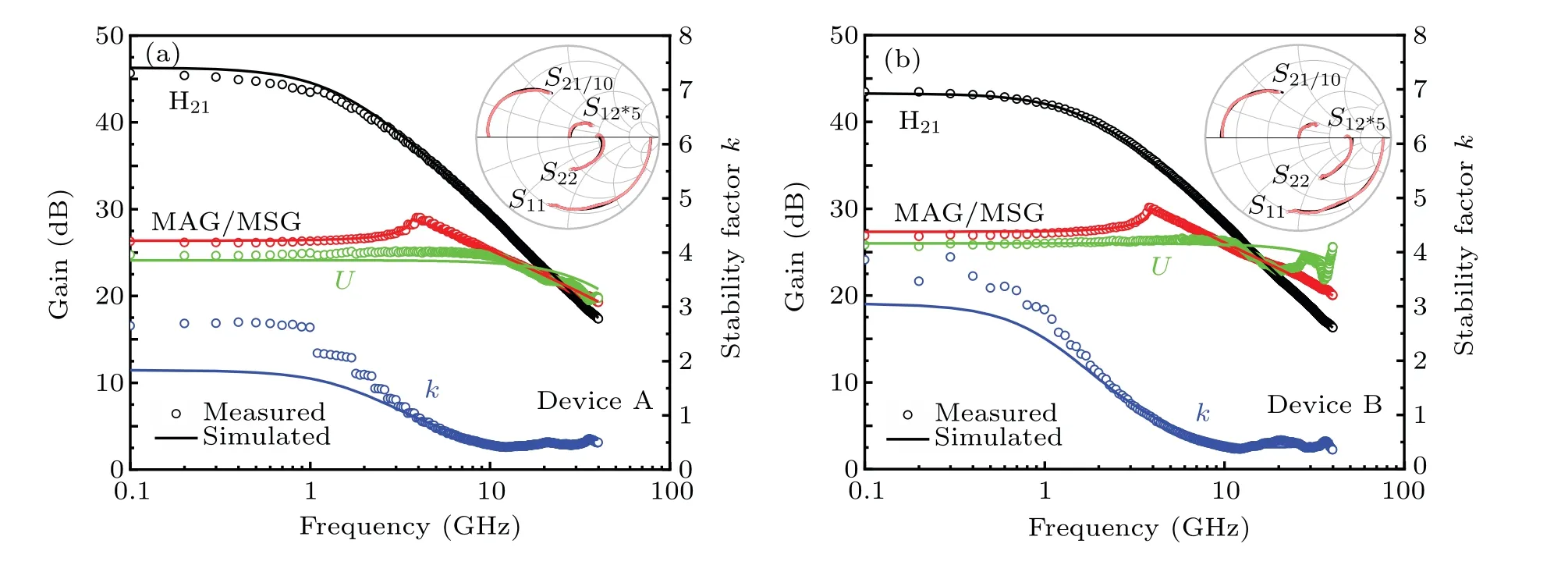
Fig.5. Measured(symbols)and small-signal modeled(lines)RF gains(H21,U,MAG/MSG)and stability factor(k)of the single and double recessed HEMTs.

Table 2. The parameters of the small-signal equivalent circuit of devices.
Table 2 summarizes the small-signal modeling parameters of the single and double recessed HEMTs, and also includesfT,measfor comparison. The measured(fT,meas)and the modeledfT(fT,model)are very similar,increasing the credibility of our analysis. Equations(2)and(3)suggest thatCgs,Cgd,Rs, andRdare the key parasitic parameters that affectfTandfMAX.[21]The heavily doped In0.53Ga0.47As/In0.65Ga0.35As cap layers are partially removed in the etching process of the first gate recess, which significantly increases the series resistances (RsandRd), resulting in thefTof double-recessed HEMTs being lower than that of the single-recessed HEMTs.On the other hand, double-recessed HEMTs achieve greaterfMAXdue to the decrease inCgdandgds. The decrease ofgdsis attributed to the effective suppression of impact ionization by the double recess structure.[22]
3.2. Gate offset in the first gate recess
The performances of double-recessed HEMTs with different gate offsets are compared. The gates of devices B, C,and D are located in the middle of the first gate recess,toward the source or toward the drain,respectively. The drain-side recess length(Lrd)of devices B,C,and D are 0.35 μm,0.6 μm,0.1 μm, respectively, while the width of the first gate recess remained 2.4 μm.
Figure 6 shows theID–VDoutput characteristics and transfer characteristics of the devices B, C, and D. WhenLrdincreased,namely,gate position shifted from drain side to source side in the first gate recess, bothID,maxandgm,maxincreased.Device C shows the highestID,maxof 1038 mA/mm andgm,maxof 1151.6 mS/mm.
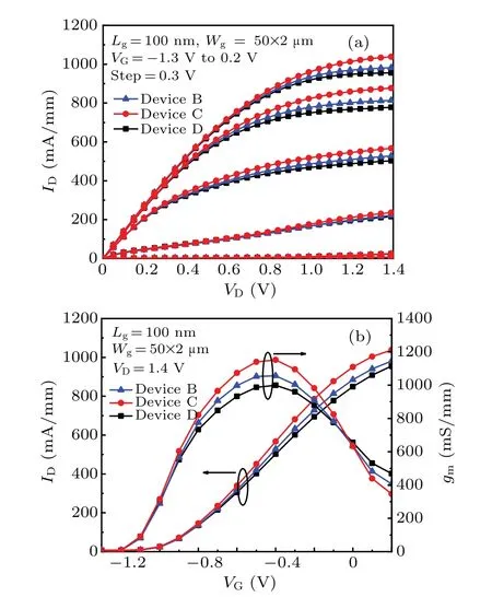
Fig. 6. DC output (a) and transfer (b) characteristics of devices B, C,and D.
Figure 7 shows the H21and MAG/MSG versus frequency of devices B,C,and D atVG=-0.4 V andVD=1.4 V.As the gate position shifts from drain side to source side in the first gate recess,fTdecreases from 287 GHz to 258 GHz andfMAXincreases from 342 GHz to 425 GHz. To explain the variation of RF performance,the parameters are extracted based on the small-signal model,as shown in Table 3.

Fig.7. The H21 and MAG/MSG versus frequency of devices B,C,and D.

Table 3. The parameters of the small-signal equivalent circuit of devices.
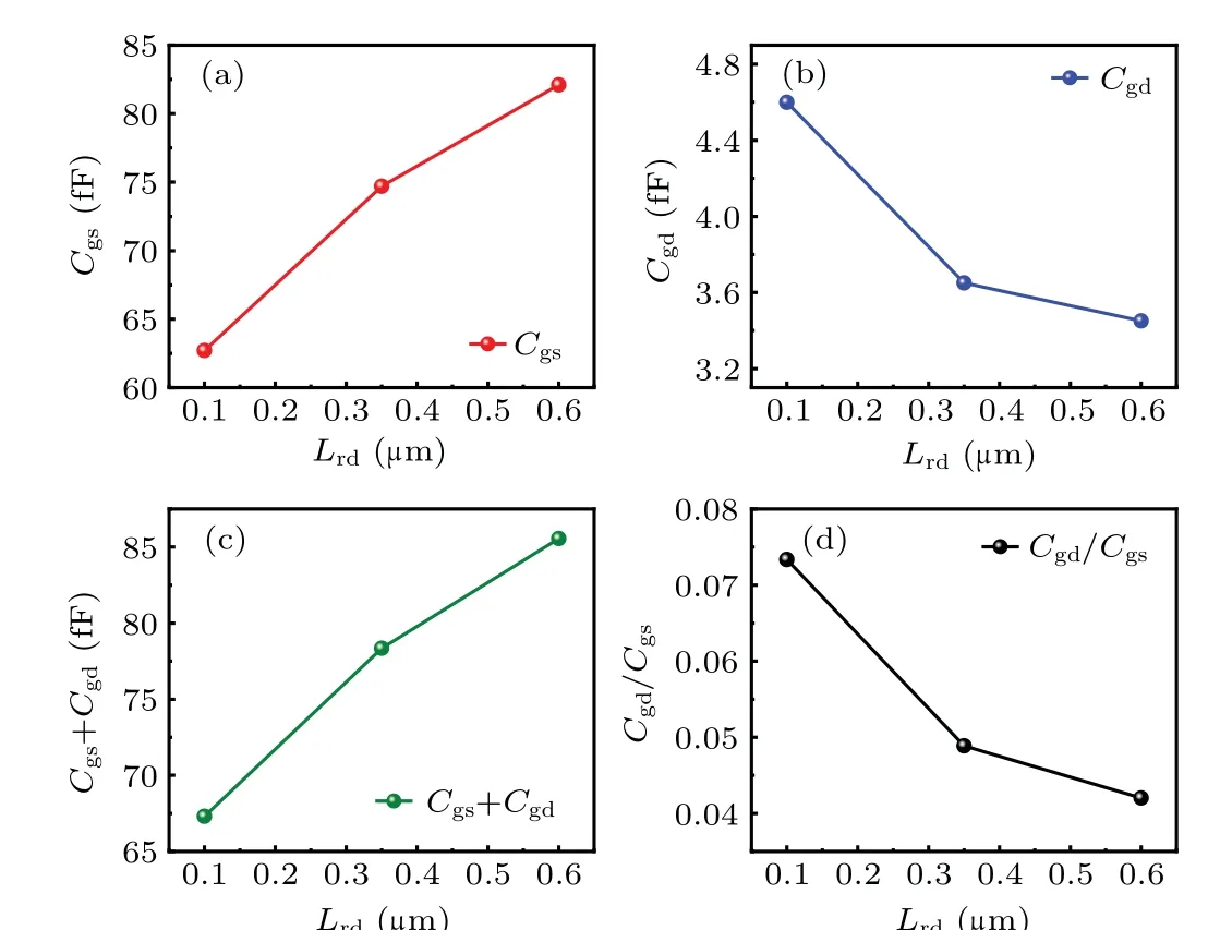
Fig.8. Dependence of Cgs(a),Cgd(b),Cgs+Cgd(c)and Cgd/Cgs(d)on Lrd for double-recessed HEMTs.
Figure 8 shows some key parasitic parameters as the functions ofLrd. The parametersCgsandCgdwere extracted by Eqs.(4)and(5). TheCgsincreased andCgddecreased by extendingLrdfrom 0.1 μm to 0.6 μm, as shown in Fig. 8. Although the changes ofCgsandCgdwith the extension ofLrdare not the same, the increase ofCgs+Cgdwell explains the observed decrease offT. On the other hand, since the opposite changes ofCgsandCgdlead to the further reduction ofCgd/Cgs, the device C with the gate offset to the source side exhibits a maximumfMAXof 425 GHz. Compared with the single-recessed HEMTs (device A) withfMAXof 355 GHz,the increase offMAXis about 20%.

Table 4 summarizes the reported performance of InP HEMT devices with a gate length of about 100 nm.Our device exhibits outstandingfMAXin devices with gate length over 100 nm by using double-recessed offset gate process technology. The device performances can be further improved by reducing the gate length or using InAs-rich channel materials in the future.
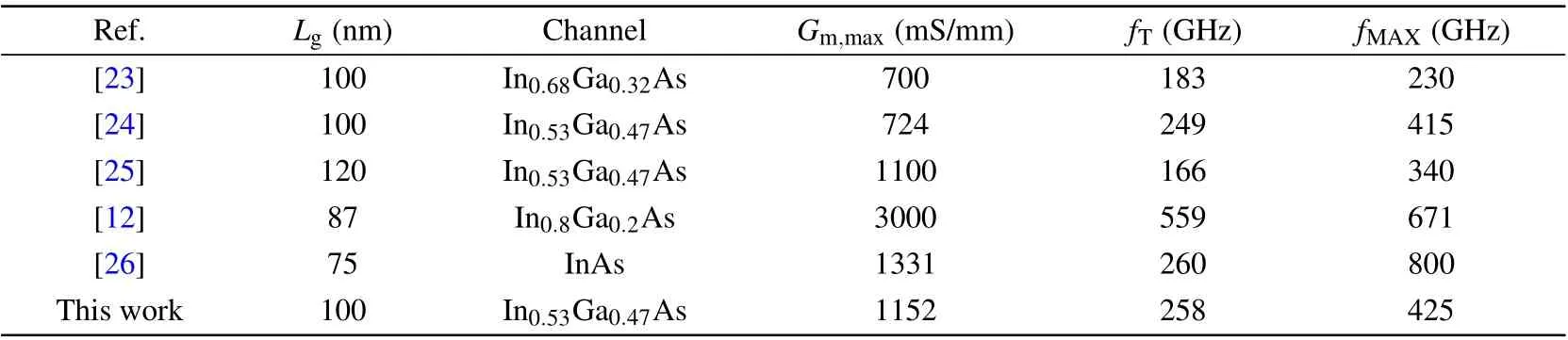
Table 4. Compared with the published InP HEMT with a gate length of about 100 nm.
4. Conclusion
In summary we demonstrated a novel double-recessed offset gate process for InP HEMTs. The double-recessed HEMTs can effectively improvefMAXby reducinggdsandCgs. With the gate offset from the drain side to the source side,fMAXcan be further improved by suppressingCgd/Cgs. Finally,thefMAXof double double-recessed offset gate HEMTs is 20%higher than that of single-recessed HEMTs.
Acknowledgements
This work is supported by the National Natural Science Foundation of China (Grant Nos. 61874036, 62174041, and 61434006),the Open Project of State Key Laboratory of ASIC and System (Grant No. KVH1233021), the Opening Foundation of the State Key Laboratory of Advanced Materials and Electronic Components(Grant No.FHR-JS-201909007),the Guangxi Innovation Research Team Project (Grant Nos. 2018GXNSFGA281004 and 2018GXNSFBA281152),the Guangxi Innovation Driven Development Special Fund Project(Grant No.AA19254015),and the Guangxi Key Laboratory of Precision Navigation Technology and Application Project(Grant Nos.DH201906,DH202020,and DH202001).
猜你喜欢
Chinese Physics B(2022年10期)2022-10-26
小哥白尼(野生动物)(2022年5期)2022-08-15
科海故事博览·上旬刊(2022年5期)2022-05-17
Plasma Science and Technology(2021年11期)2021-11-30
幼儿智力世界(2019年12期)2019-10-26
电影(2018年12期)2018-12-23
速读·下旬(2017年4期)2017-06-20
小学阅读指南·低年级版(2009年4期)2009-05-13
数学大王·中高年级(2006年7期)2006-07-01
- Chinese Physics B的其它文章
- A nonlocal Boussinesq equation: Multiple-soliton solutions and symmetry analysis
- Correlation and trust mechanism-based rumor propagation model in complex social networks
- Gauss quadrature based finite temperature Lanczos method
- Experimental realization of quantum controlled teleportation of arbitrary two-qubit state via a five-qubit entangled state
- Self-error-rejecting multipartite entanglement purification for electron systems assisted by quantum-dot spins in optical microcavities
- Pseudospin symmetric solutions of the Dirac equation with the modified Rosen–Morse potential using Nikiforov–Uvarov method and supersymmetric quantum mechanics approach